MASSACHUSETTs
OF
TECHN'OLOGYINIfTflE
CAD Enabling Smart Handtools
by
OCT
3
0
201
LIBRARIES
Pragun Goyal
Submitted to the Program in Media Arts and Sciences,
School of Architecture and Planning,
in partial fulfillment of the requirements for the degree of
Master of Science in Media Arts and Sciences
at the
MASSACHUSETTS INSTITUTE OF TECHNOLOGY
September 2014
Massachusetts Institute of Technology 2014. All rights reserved.
Signature redacted
A uthor ...
...
Program in WVediArts and Sciences,
School of Architecture and Planning,
August 8, 2014
Signature redacted
C ertified by ...
...Joseph A. Paradiso
As ceProfessor of Media Arts and Sciences
Program in Media Arts and Sciences
Thesis Supervisor
Signature redacted
A ccepted by ...
...
. Patricia Maes
Interim Department Head
Program in Media Arts and Sciences
CAD Enabling Smart Handtools
by
Pragun Goyal
Submitted to the Program in Media Arts and Sciences, School of Architecture and Planning,
on August 8, 2014, in partial fulfillment of the requirements for the degree of
Master of Science in Media Arts and Sciences
Abstract
CAD (Computer Aided Design) software allows one to describe a design in great detail
and at any arbitary scale. However, our interface to CAD is still largely through traditional avenues: screen, keyboard and pointing devices. While these interfaces function for their intended purposes: text entry, pointing, browsing, etc, they are not designed for the purpose of mediating the flow of information from and to a physical workpiece. Traditional input interfaces are limited in the sense that they lack a direct connection with the workpiece, forcing the user to translate information gathered from the workpiece before it can be input into the computer. A similar disconnect also exists in the realm of output from the computer. On one extreme, the screen as an output interface forces the user to interpret and translate information conveyed graphically to the context of the workpiece at hand. On the other extreme, devices like CNC machines and 3D printers lack a way for the user to engage with the fabrication and to iteratively change design parameters in realtime.
In this work, I present, two handtools that build on the philosophy of Free-D ([1]
and [2]), a smart milling tool recently developed in our research group. to create a similar interface between Computer Aided Design and the physical workpiece, in en-tirely different application domains. The two handtools are BoardLab and Nishanchi. BoardLab is a smart, context-aware oscilloscope probe that can be used to dynami-cally search for just-in-time information on electronic circuit board design data and to automatically annotate the design data with measurements and test data. Nishanchi is a handheld inkjet printer and 3D digitizer that can be used to print raster graphics on non-conformable surfaces.
Thesis Supervisor: Joseph A. Paradiso
Title: Associate Professor of Media Arts and Sciences Program in Media Arts and Sciences
The following people served as readers for this thesis:
Signature redacted
Thesis Reader ...
...
Prof. Patricia Maes
Alexander W. Dreyfoos (1954) Professor
Program in Media Arts and Sciences
Signature redacted
Thesis Reader ..
Amit Zoran
Post-doctoral Associate
Fluid Interfaces Group
Program in Media Arts and Sciences
Acknowledgments
I am thankful to Prof. Joe Paradiso, Amit Zoran and Prof. Pattie Maes for their feedback as readers. Thanks to Amit for helping me develop my own understanding of the role that technolgy plays in our lives and for always giving me insightful design critique on my work. Thanks to my parents, Isha, Lina, Amna and Anirudh for moral support and encouragement. Special thanks to Lina for help in making this thesis so much more understandable and cleanly written. I am thankful to my parents, Isha and Wooly for tolerating my long absence from home while I was pursuing the work in this thesis.
Contents
1 Introduction 191.1
Related Work . . . .. . . . .
20
2 BoardLab
23
2.1 Introduction . . . ..232.2
Related work . . . .
26
2.3 Design and technology . . . 26
2.3.1 Tracking system. . . . 27
2.3.2
PCB layout digestor . . . .
28
2.3.3 Probe tip projection on the PCB . . . 32
2.3.4 The rest of the system . . . 33
2.4 Operation and interaction . . . 36
2.4.1 Board positioning mode . . . . 36
2.4.2 Component selection Mode . . . . 37
2.4.3 Voltage annotation mode . . . . 37
2.4.4 Waveform verification mode . . . 38
2.5
Design history . . . .
38
2.5.1 First prototype: Camera based tracking, KiCAD . . . 39
2.5.2 Second prototype: Magnetic tracking, Eagle . . . . 39
2.6 Discussion and future work . . . . 41
3 Nishanchi
45
3.1 Introduction . . . 453.1.1 Printing on non-conformable surfaces 3.2 Printing CAD design parameters .
3.3 Related work . . . . 3.4 Design and technology . . . . 3.4.1 Handset design . . . . 3.4.2 Inkjet printing system . . . 3.4.3 Tracking system . . . .
3.4.4
Digitizing tip . . . .
3.4.5 Inkjet nozzle(s) position and 3.5 Software . . . .. 3.6 Operation and interaction . . ..
3.7 Digitizing mode . . . .
3.8 Print mode . . . . 3.9 Overall workflow . . . . 3.10 Design history . . . . 3.10.1 First prototype . . . . 3.10.2 Second prototype . . . . 3.10.3 Third prototype . . . . 3.10.4 Fourth prototype . . . .3.10.5 Printing in 2D: Guy Fawkes
3.10.6
Quantitative
analysis . . 3.10.7 User impressions . . . . 3.10.8 Conclusions.. . . .3.11 Printing in 3D . . . .
3.11.1 Printing decorative patterns 3.11.2 Printing CAD parameters . 3.11.3 Impressions . . . . 3.12 Discussion and future work.. . . 3.12.1 Future work . . . .
orientation
mask . .
4 Summary and conclusions 83
4.1 Learnings . . . 83
4.1.1 Workpiece re-registration . . . 84
4.1.2 Software framework . . . 84
List of Figures
2-1 BoardLab conceptual diagram . . . 23
2-2
. . . .
24
2-3 An overview of the Boardlab system . . . 27
2-4 The PCB digester highlights the via selected for PCB positioning
.
.
29
2-5 Pointcloud for sensor positions while the probe pin is fixed at a via (the center of the sphere) . . . 33
2-6 Left: BoardLab PCB feature map for a PCB layout. Green rectan-gles show PCB components, and blue rectanrectan-gles show component pins. Right: The same PCB layout file as displayed in the Eagle 6.0 Lay-out editor. Notice the more pleasing and legible color scheme used in
BoardLab :) . . . .
34
2-7 The probe position tracked on the PCB feature map . . . 34
2-8 Diagram showing how different parts of the BoardLab system are con-nected. ... ... 35
2-9 The final version of the probe disassembled to show internal assembly 35 2-10 PCB symbol selected on the PCB feature map . . . 36
2-11 Schematic symbol selected on schematic display . . . 37
2-12 The first prototype of BoardLab using camera and AR fiducials to track the probes. Left: Complete system with camera and stand. Right:
Probes with AR fiducials . . . .
38
2-13 The first design of the probe. . . . 40
2-14 The first revision of the probe . . . 40
2-16 Probe revisions for the second prototype of BoardLab using magnetic tracking system . . . 40
3-1 Nishanchi concept graphic. The similarity of the device with the shape
and size of a typical hand-launched grenade is purely coincidental. . . 45 3-2 Photographs showing how design parameters from the 3D CAD model
of a stool are transferred manually to the workpiece.. . . . 47 3-3 Sheetmetal worker cutting a sheet of aluminum with which to roll a
cylinder. The distance of the mark from the top edge of the sheet de-termines the height of the cylinder and length of the section dede-termines the diam eter. . . . 48 3-4 Nishanchi system overview . . . 49 3-5 Photograph of the printhead control circuit board mounted on the
handset . . . 50 3-6 Scan of a print showing alternate white and dark bands because of the
onboard FTDI buffers. Contrast this with figure 3-9 which was printed
by tuning the USB FTDI buffers as described in section 3.4.2. ....
51
3-7 CAD model of the final prototype showing X and Z components for
nozzle offset vector . . . . 53 3-8 Photograph of the final prototype showing Z component measurement
for nozzle offset vector . . . 53 3-9 The Red and Black circles in this printout were printed by
translat-ing the handset in generally one orientation throughout the printtranslat-ing process for each circle, respectively. The handset was rotated by 90 degrees in the plane of the printout between the two colors. The dis-placement between the two circles shows the error in the nozzle vector values. . . . 54 3-10 Two-lines calibration print . . . .. 55
3-11 Calibration print showing broken displaced lines when connected parts of the lines are drawn keeping the handset in the orientation as shown
by the blue arrows. . . . . 55
3-12 Post calibration print. Left: Printing across the line direction. Right: Printing across the line direction. The Red and Black sections differ in handset orientation by 180 degrees as shown by blue arrows.. . . . 56
3-13 A photograph of a user using Nishanchi (final prototype) to make a print on paper. . . . . 57
3-14 Nishanchi first prototype . . . . 59
3-15 The software for Nishanchi first and second prototypes. Cyan colored pixels have already been printed and the black pixels are yet to be printed. The red vertical cursor is the estimated position of the inkjet nozzles with respect to the image. . . . . 60
3-16 The second prototype. Notice the magnetic tracking sensor and the blue overlay. . . . . 61
3-17 A section of the Guy Fawkes' Mask printout showing artifacts intro-duced by the user's movement of the handset. This print was made using the second prototype. . . . .. 62
3-18 The solidworks CAD model of the handset showing internal chassis that mounts the circuit boards, buttons, tracking sensor, digitizer and printhead. . . . . 63
3-19 3D printed third prototype . . . . 63
3-20 ...
64
3-21 ...
...
64
3-22 ....
...
.
.
...
...
64
3-23 CAD models of different handset designs before the third prototype, shown in figure 3-19 . . . . 64
3-24 The original image used for Guy Fawkes mask . . . . . 65
3-26 Plot showing the analyzed tool usage data for user Santiago. Section 3.10.6 describes this figure in detail . . . 67 3-27 Top left: Santiago's print. Top right: Visualization of handset position
data. Bottom: Visualization of usage data. . . . 68 3-28 Top left: Alexis's print. Top right: Visualization of handset position
data. Bottom: Visualization of usage data. . . . 69 3-29 Top: Amit's print. Top right: Visualization of handset position data.
Bottom: Visualization of usage data. . . . 70 3-30 Top: Nan's print. Top right: Visualization of handset position data.
Bottom: Visualization of usage data. . . . 71 3-31 Top: Gershon's print. Top right: Visualization of handset position
data. Bottom: Visualization of usage data. . . . 72 3-32 Top: Julie's print. Top right: Visualization of handset position data.
Bottom: Visualization of usage data. . . . 73 3-33 A screenshot of the hemispherical model of the bowl and the supporting
plane as created in Rhinocerous using the point cloud data.. . . . . . 76 3-34 The 2D vector art used to render printed surfaces on the bowl. . .... 77 3-35 The bowl printed using Nishanchi with the design derived from figure
3-34. ...
...
78
3-36 The original Yanien sculpture mated with the Ikea bowl as base. . . . 79
3-37 ...
...
79
3-38 Screenshots showing the computation of the intersection curve (blue) between the lower section of the Yanien sculpture (red) and the bowl
(black).
. . . .
79
3-39 A photograph of the bowl before cutting along the lines made on it
using Nishanchi . . . .
80
4-1 Diagram showing simplified information flow in a traditional hand fab-rication workflow using CAD. The user mediates the flow of informa-tion between the computer and the tool. . . . 85 4-2 Diagram showing simplified information flow in a fabrication workflow
using CAD and computer controlled automatic machines (for example CNC mill, 3D printer,etc). The computer blocks the user out from engaging in the actual fabrication process. . . . 85 4-3 Diagram showing the new simplified information flow. The smart tool
Chapter
1
Introduction
An excellent survey of smart tools is given in [3]; here I highlight a few particular
examples to stimulate the discussion. SketchPad [4] was probably one of the first
applications of computing to create, edit, and store graphic designs. Now, CAD
(Computer Aided Design) softwares allows one to describe a design in great detail
and at varying scales. However, the interaction with CAD software is still largely
through traditional interfaces: screen, keyboard and pointing devices. While these
interfaces function for their intended purposes - text entry, pointing, browsing, etc.
They are not designed for the purpose of mediating the flow of information from and
to a physical workpiece. Traditional input interfaces are limited in the sense that they
lack a direct connection with the workpiece, forcing the user to translate information gathered from the workpiece before it can be input into the computer. A similar disconnect also exists in the realm of output from the computer. On one extreme, the screen as an output interface forces the user to interpret and translate information
conveyed graphically to the context of the workpiece at hand. On the other extreme
are devices like CNC machines and 3D printers - while these devices maintain a
high-bandwidth connection with the workpiece, they completely lack a way for the user to
engage with the fabrication and to iteratively change design parameters in realtime.
Handtools have been traditionally used throughout the history of mankind for
fabrication. A traditional handtool acts as an interface between the user and the workpiece. Inspired by Free-D [1] and [2], which acts as an adaptive interface between
the computer, the user and the workpiece, I present, two handtools that build on the philosophy of Free-D to bring a seamless interface between Computer Aided Design and the physical workpiece to these applications. The two handtools are BoardLab and Nishanchi. BoardLab is a smart context-aware oscilloscope probe that can be used to search for just-in-time information of electronic circuit board design data and to annotate the design data with measurements and test data, both dependent on the circuit element or node being probed. Nishanchi is a handheld inkjet printer and 3D digitizer that can be used to print raster graphics on non-conformable surfaces.
In both projects, the position and orientation of the tool is tracked with respect to the workpiece. A computer uses the tool position and orientation with a CAD model of the workpiece and actuates the tool automatically depending on the mode of operation and user-triggered events. This allows for the user and the handtool to interact with the workpiece in a tight choreography, leveraging craft skills as when exploiting a conventional handtool, while still maintaining a realtime connection with the computer model of the workpiece.
1.1
Related Work
There have been a number of smart tools built for different specific applications. The Wacom tablet and pen
[5],
and the Anoto digital pen [6] allow the user to write on paper while digitizing the input at the same time. The flow of information in these tools is mainly from the workpiece to the computer. Kim et al. present a way of using a computer controlled pencil to allow the user to create sketches on paper [7]. Junichi et al. present another approach to a hybrid pen-paper interaction where the tip of the pen is actuated by computer controlled magnets [8]. These tools demonstrate how, within the realm of sketching using pen/pencils, a handtool can mediate the flow of information from the computer to the workpiece and vice versa.The same philosophy is exemplified in the realm of painting and digital painting by I/O Brush [9], Fluidpaint [10] and Intupaint [11]. I/O Brush uses images and videos taken at a close range from everyday objects to create a final graphic. Fluidpaint
and Intupaint allow the use of conventional brushes in digital medium. Baxter et al. simulate the forces felt while brushing using actuation to allow users to express themselves creatively in the digital painting medium [12]. These tools allow the user to be much more expressive in painting in the digital medium; however, it is not clear how the digital medium aids the user in the creation of a physical artifact.
In the realm of 3D object creation, tools like the Creaform 3D Handheld Scanner [13] allow the user to create a 3D model of an existing workpiece. Song et al. describe an approach in which annotation marks made on the workpiece instruct changes to a computer 3D model [14]. However, in these approaches, the tool does not help in translating the changes expressed on the computer back to the workpiece.
My work is closest in spirit to Free-D ([1] and [2]), and the work done by Rivers et al. [15]. However, one of the key difference is that both BoardLab and Nishanchi are designed to work with existing semi-complete or complete artifacts. In the case of Boardlab, a description of the electronic circuit is loaded into the software in the form of the PCB layout and the schematic data. In the case of Nishanchi, the digitizing tip allows the user to input relevant parameters about the workpiece into the CAD software. The projects also differ from ([1], [2] and [15]) in that the output of the tool is in the form of design information rather than a fabricated workpiece.
2
*1 r""
l .,
~4r-
41
Figure 2-1: BoardLab conceptual diagram
2.1
Introduction
Use of Electronic Design Automation (EDA) software has become quite popular in the design of Printed Circuit Boards (PCBs). A very common paradigm is to design the schematics first and then convert them to a PCB layout. The resulting PCB layout can then be fabricated and assembled with electronic components. Access to the schematic design data of a PCB is quite helpful while testing and assembling a PCB, because such data gives the user a good idea of how the components are connected. This becomes even more important while debugging a PCB or while diagnosing a PCB's faults.
Chapter
BoardLab
,.,.
E
A typical electronics workspace. Notice the two displays in front of the user that display schematic diagrams and the PCB layout.
The screen on the left is being used to display schematics and the screen on right to display source code.
Other screens in the workspace:
oscil-loscope and multimeters.
Figure 2-2
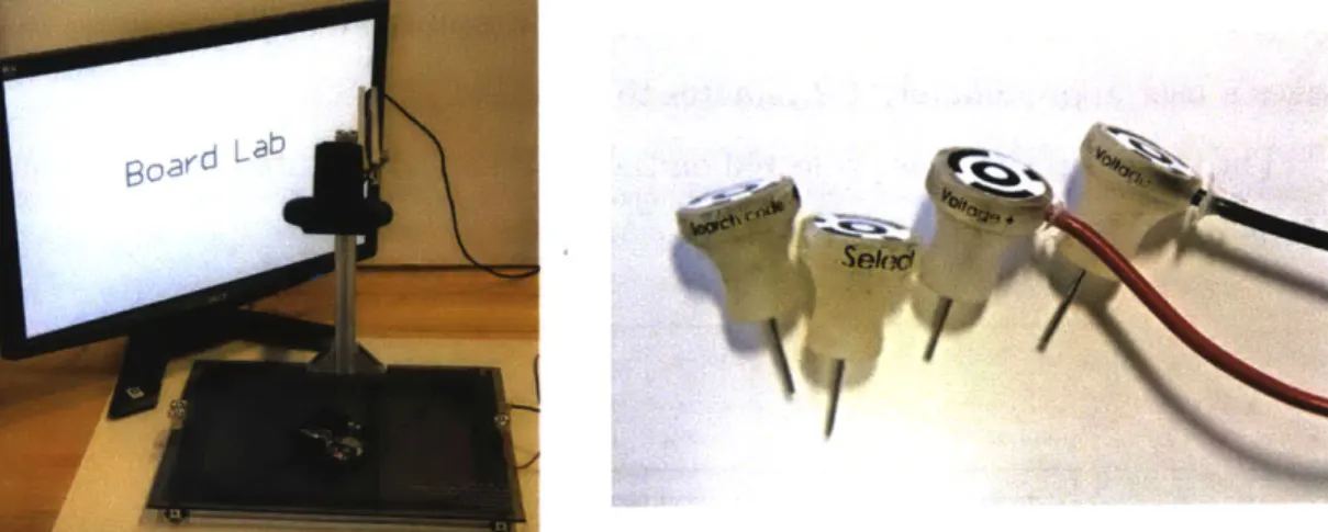
Although production testing of commercial scale PCBs generally employs a custom made multi-wire probe that automatically engages strategic testpoints on the board. The boards are usually extensively manually probed while being tested and debugged,
While most modern EDA software offers an easy-to-use WYSIWYG (What You See Is What You Get) interface, the keyboard and mouse interface required to query and annotate design data on EDA software creates a disconnect in the workflow of manually debugging or testing a PCB. This is because most operations and tools used in this process involve working directly with the circuit board and its components. However, in order to locate a component in the schematic or in the PCB layout, the user has to try to find a visually similar pattern in the PCB layout file, or else key in the identifier for the component read from the PCB silkscreen annotation. Both of these processes are cumbersome and lead to unnecessary cognitive load. Fig 2-2 shows a photograph of a typical electronics design and prototyping workspace with two display screens dedicated to displaying the schematics and PCB layout, respectively, plus another showing real-time waveforms from the node being probed. Small component sizes and similar looking components further magnify the associated confusion.
Experienced electronics designers often partially work their way around this by annotating the board with design data, including descriptors, part-numbers, compo-nent values, etc. However, the board space limits the amount of design information that can be embedded in the annotations. Also, this approach does not work well for denser electronic circuits.
The BoardLab system consists of a handheld probe that allows for direct inter-action with the board and board components for just-in-time information on board schematics, component datasheets, and source code. It can also take voltage mea-surements, which are then annotated on the board schematics. The emphasis is on providing the same kind of interaction with the PCB as is afforded by other commonly used tools, like soldering irons, multimeters, oscilloscopes, etc. Figure 2-1 illustrates how the BoardLab System becomes a way to introspect and annotate the design data using the actual circuit board as the interface. The system supports the following modes:
1. Board positioning mode 2. Component selection mode
3. Voltage annotation mode 4. Waveform verification mode
These different modes are detailed in the following sections.
2.2
Related work
Previous work to provide just-in-time information about electronic circuits involves the use of tagged components, enabling their positions to be tracked in the circuit [16]. However, this technique requires specially constructed components. BoardLab builds on the high-level approach described in [17], where pointing gestures are used to index information tagged with different objects. BoardLab uses a handtool form factor, which allows for pointing at small components on a circuit more accurately. The design of BoardLab has been inspired and informed by the design of of FreeD [2], where a position-orientation tracked handtool provides for interaction with both the physical work piece and the design data at the same time. This approach is also
similar to the one described by Rosenberg et al. in [18], where a position-orientation
tracked probe is used to verify component positions on a circuit board. The difference, however, is the reuse of design information for the board, which allows for further extension into signal verification and code-introspection.
2.3
Design and technology
Boardlab is designed to be used just like other standard benchtop electronics instru-mentation. The user employs a handheld probe to introspect and to make
measure-ments on the circuit board. A computer runs the BoardLab software and displays
the results on a screen. A tracking system tracks the position and orientation of the probe as the user engages it. As essentially all modern PCBs are generated in an ECAD system that generates a precise mechanical model of the circuit board, node, trace and component placement can be straightforwardly input to BoardLab.
Circuit board
Display
Multimeter
mill
III.
Tracking system
TransmitterU
ComputerL9u
Figure 2-3: An overview of the Boardlab system
2.3.1
Tracking system
The handheld probe is augmented with a MMTS (magnetic motion tracking system) sensor that allows for tracking of the 3D position and 3D orientation of the probe. A Polhemus FASTRAK system (an AC 6D magnetic tracking system
[19])
is used to estimate the 3D position and 3D orientation of the probe using a sensor mounted on the probe. The position and orientation state given by the tracking system is translated to get the position of the tip in the reference frame of the workbench. The Polhemus system can be configured to output the orientation data as a quaternion. The following equation is used to get the position of the tip (rtip,tx,tx) with respect to the transmitter (tx), in the reference frame of the transmitter (tx).rip,tx,tx = rrx,tx,tx + M * frtip,rx,rx
(2.1)
where rip,rx,rx is the vector from the receiver (rx) on the probe to the tip (tip) of the probe in probe reference system (rx), and M is the 3x3 rotation matrix derived
Probe
from the orientation quaternion given by the tracking system.
While the CAD design of the probe could be used to compute the vector that connects the sensor origin to the tip's endpoint, I found that because of 3D printing tolerances and slight misalignment of the sensor on the probe, it is better to calibrate for the vector. The following procedure is used to collect calibration data:
1. The tip of the probe is held fixed to a via (e.g. through-hole) in the board. 2. The probe is moved around making sure that the tip is always touching the via.
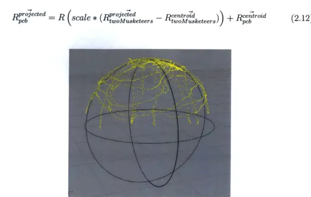
Assuming that the sensor is rigidly mounted on the probe, and ignoring the small movement of the tip within the via, the resulting set of position points should lie on the sphere centered at the via and with a radius equal to the vector (ri,,,,). The center (center) and radius (rip,rx) of the sphere can be found by importing the point cloud in a CAD program (Rhinocerous) and fitting a sphere to the points. The radius given by the CAD program is the modulus of the vector needed to be computed for calibration. The following equation gives the the rtx for point i in the pointcloud in the reference frame of the transmitter (tx). However, as we have the orientation information for each point, we can apply the inverse of the rotation matrix derived from the orientation quaternion for each point to get the i%. The following equation
illuminates the way.
r,=
M-1'Z * rx (2.2)The mean rip,,. for all i gives the calibration rtip,rx. I found that applying a linear RANSAC (RANdom SAmple Consensus) filter to the pointcloud eliminates erroneous data that could be introduced by accidentally moving the probe out of the via during calibration data collection.
2.3.2
PCB layout digestor
The PCB layout digestor, as the name suggests, is the pythonic entity responsible for parsing of the PCB layout file for the circuit board, and to track the projected
position of the probe tip on the PCB layout. Needless to say the PCB layout also has to deal with errands like understanding what orientation and position the PCB is placed at on the workbench. The following section describes the position and orientation estimation of the PCB.
PCB position estimation
Given that most electronic circuit boards are rigid and planar, it is relatively safe to assume that the PCB is of planar geometry. We can estimate the 3D position and orientation of the PCB by using the probe tip to estimate the 3D positions of three or more known vias on the PCB. For the sake of completion and intellectual stimulation, the implementation of the algorithm as originally described in [20] is detailed below.
00 00000000 .00000000 00 00 ,.. - - Selected Via -
-*
l0*..
O. 00'o 000a -00.- - * I O00 000.0Figure 2-4: The PCB digester highlights the via selected for PCB positioning
The following procedure is used to collect PCB position estimation data: 1. The software picks three (or more) pre-defined vias (Figure 2-4).
2. The user respectively pushes the tip into the via and holds the probe in that position for about 5-7 seconds. The system collects the estimated position data for the probe tip as this is done.
While the PCB position and orientation could be described as a 3D position and 3D orientation, as the PCB features are described as 2D features on the PCB plane, it seemed appropriate to represent the PCB position and orientation as a 2D object on a 3D plane. This would allow the positions of the features of the PCB to be used in their native reference system.
The 3D plane (Px) is found in the reference frame of the transmitter using a simple
least squares fit on the via position data. However, this plane is still represented in
the frame of the transmitter. We need to find a reference frame such that one of the major planes of the reference frame is co-planar with the PCB plane; this allows us to move from 3D position to 2D position on the PCB plane by the means of a
simple transformation. In order to do that, we need to find three orthonormal unit
vectors ThreeMusketeers such that two of them lie in the PCB plane. The following technique is used to find three orthonormal basis vectors.
1. Let Athos, Artagnan be two of the three lines formed between the three vias selected for calibration. Athos forms the first of the three orthonormal unit vectors.
2. Pathos = Athos x Artagrnan gives Pathos, the second element of ThreeMusketeers.
3. The third element of Arhemis is found to be Pathos x Athos.
Notice, that Athos and Arhemis are in the plane of the PCB, and Pathos is
normal to it. Also note that the three vectors are represented in the reference frame
of the transmitter. Any of the three arbitrary vias can be selected as the origin of the new reference frame riuckyvia,tx. Now, the representation of a position of a point p in this new reference frame can be computed as
Rp,ThreeMusketeers =
[Athos,
Pathos, Arhemis] x ( - ruckyvia,tx)(2.3)
Further, for points on the PCB plane, the component corresponding to Pathos can be dropped, giving us a convenient 2D representation. However, we still need to com-pensate for the scale, translation, and rotation between the PCB layout 2D frame of reference pcb and the 2D frame of reference fixed on the PCB plane: twoMusketeers.
Let the rTwoMusketeer,
be the position of a via in the twoMusketeers, and rt
be
the corresponding position in the PCB layout. The scaling can be obtained by simply comparing the mean distances between vias in both frames of reference,
si,jE(1,2,3),ifj (Irc pc-II)(
scale = . . . , (2.4)
mean _,mean
i,jE(1,2,3),ij
(IrwoMusketeers
oMusketeers)where
rmoe
ee is the mean of all position estimates for via i.The translation rji is obtained as the translation between the centroids of the scaled estimated position pointclouds and PCB layout via position pointclouds. The centroid for the pointcloud can be computed as:
r.= rcentrod scale * rcentroid
(2.5)
fix~ r pd twoMuskceteers
(5
The centroids can be found using the following equation:
rcentroid = (2.6)
n
The rotation can be obtained as follows:
1. Compute vectors for each via position centered around the centroid.
at
= r - rcentred,(2.7)
and
bi= scale
* (r woMusketeers - rtwousketeers), (2'8)2. Compute the 2 x 2 covariance matrix as:
S = XIYT
(2.9)
where, X, Y are 2 x n matrices with ai and b as their columns. I is a 2 x 2 identity
3. Compute the singular value decomposition S = U E VT. The 2D rotation
matrix is then obtained as:
R =VUT
(2.10)
At the end of PCB position estimation, the three parameters that define the position and orientation of the PCB are scale, rfix, and R. Of course, the board needs to be rigidly held relative to the workbench during the process, otherwise another calibration needs to be performed. Conversly, another tracking device can be rigidly mounted to the board as well although with the Polhemus system, care needs to be taken of distortion from connections or ferros material in proximity to the sensors and EMI.
2.3.3
Probe tip projection on the PCB
The previously described values scale, r1 fx, and R are used to project the probe tip
position along the probe vector onto the PCB plane. The projected point is then transformed to the PCB layout reference system.
1. The projection of the probe tip on the PCB plane along the probe vector is:
Roected = Rtx -t (rtp -
Rgij
) -Pathostx)Pathostx,
(2.11)where R" *jected is the projected point and R "i" is the origin of the PCB plane, both expressed in the reference frame of the transmitter tx.
2. The RQoJected is transformed to the threeMusketeers frame of reference RJ e
using equation 2.3.
3. The Pathos
component
of Rr.*ee,,ted , isdropped
to obtain the 2Dpoint
Rth e se o e ,te ,
o
n th
e P
C
B la n
e .
4. The R *ouu ,,eteers is transformed to PCB layout reference frame Rcb by ap-plying the scale, r fix and R as computed in the previous subsection, as,
Rpoece
(sal
R.
R-+ece)cnro
) + Rcenr (2.12)Rpgee
(sal
Rwo*usketeers
twoluketeers) cnrFigure 2-5: Pointcloud for sensor positions while the probe pin is fixed at a via (the center of the sphere)
PCB Feature map
The system supports two types of PCB features: components and pins. For both types of features, maximum rectangular extents are computed based on the PCB top and bottom trace layers and are mapped to active GTK+ widgets. In the event of a probe event, the PCB coordinates of the probe tip projection are checked against the extents of all features of the PCB to find which feature to delegate the probe event
to.
2.3.4
The rest of the system
A HP-34401A desktop multimeter is used to provide voltage measurements to anno-tate the schematics. The SCPI (Standard Command for Programmable Instruments) interface is used to communicate with the multimeter. [21] describes the interface in more detail.
- 00-00
00-Oo-00-0-00-00--o O O
" OO 0 DO 00' '
Figure 2-6: Left: BoardLab PCB feature map for a PCB layout. Green rectangles show PCB components, and blue rectangles show component pins. Right: The same PCB layout file as displayed in the Eagle 6.0 Layout editor. Notice the more pleasing
and legible color scheme used in BoardLab
:)
OO000000 .00000 00O
00
-i - ---- Probe tip position
01). "0 --
on
* **
-
00
. o' nnon -0 -- . C
0000000 "000000
Figure 2-7: The probe position tracked on the PCB feature map
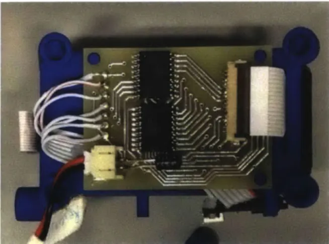
The probe (Figure 2-9) has a conductive metal tip, which is connected to the positive terminal on a desktop multimeter to make measurements. The probe tip is mounted on a spring loaded switch, which closes when the probe is pressed onto the board. The probe has another switch that can be used to cycle through different modes of operation when pressed by the thumb. The switches are connected to an Arduino microcontroller board programmed as a USB HID device. The Arduino
Probe Circuit board -Multimeter Probe Tip Tracking Tracking Sensor system I LED, Buttons Arduino Computer - - Schematics, datasheets SPICE Model - -- PCB Layout Event handler
Figure 2-8: Diagram showing how different
nected.
Mode Button
parts of the BoardLab system are
con-LED Probe spring
I
i
Probe microswitch
rI Probe tip
Figure 2-9: The final version of the probe disassembled to show internal assembly
generates computer keyboard events for switch events on the probe. The probe also
has a LED that indicates the current mode of operation. The LED is controlled by the Arduino. Figure 2-8 shows these connections conceptually.
The Arduino board, the multimeter and the tracking system are connected to
the computer that runs the BoardLab software. The software was written in python
2.7 and runs on a PC with 4GB of RAM and a quad-core Intel processor running on Ubuntu 12.04. The software parses the design of the PCB and the associated schematic from Eagle 6.0 .brd and .sch files respectively. The board file (.brd) is parsed to create a layout map of all the features of the PCB. The position and orientation of the probe is used to compute the position of the tip. The position of the tip is then overlaid on the PCB map to identify the PCB feature to which the probe is pointing.
* * OOOOOOOOO O 0~~00000000 00 00.0 aa ooo8.*II." . DODODo -0."
.0
o a' o~~ . r-- Selected Component "Uo'ooooo ooooooFigure 2-10: PCB symbol selected on the PCB feature map
2.4
Operation and interaction
The system is designed to work in the following modes: board positioning mode,
component selection mode, voltage annotation mode and waveform verification mode.
These modes are detailed below.
2.4.1
Board positioning mode
The tracking system tracks the position of the probe with respect to the work table, as the tracking system transmitter is mounted rigidly on the work table. The position and orientation of the probe need to be transformed to the coordinate system used on the circuit board. The board-positioning mode is a way for the user to tell the system where the circuit board is located on the work table.
In order to position the board, the user clicks the probe tip on three or more
preselected via holes on the circuit board. The tip position and orientation data is
then used to find the plane of the circuit board. Once the plane is determined, a least
squares 2D point cloud match is applied to calculate the displacement of the origin
the data collected from board positioning mode is obtained. This process generally
takes a user approximately 1-2 minutes to complete.
The probe tip vector is projected on the PCB plane to estimate where coordinates of the probe point on the PCB.
--Seected
Componer
Figure 2-11: Schematic symbol selected on schematic display
2.4.2
Component selection Mode
In the component selection mode, the probe allows the user to select a single
com-ponent. In this mode, the view highlights the selected component in the schematic.
The motivation is to help the user understand how the component is connected with
other components. If the component has a datasheet attribute, the view also loads
the datasheet for the component.
2.4.3
Voltage annotation mode
Over the course of testing a PCB, a user might make many measurements of voltage
across different nodes on the circuit. Conventionally, the user has had to manually
understand what a measurement made on the PCB means in the context of the
Figure 2-12: The first prototype of BoardLab using camera and AR fiducials to track the probes. Left: Complete system with camera and stand. Right: Probes with AR
fiducials
schematic. The voltage annotation mode allows for automatic annotation of the schematic with the voltage measured using the probe, together, with the expected voltage when the board is operating properly.
2.4.4
Waveform verification mode
Oftentimes, circuit board design allows for simulating sections of the circuit board to generate expected waveforms. In the waveform verification mode, the expected waveform at the measurement point is plotted with a graph of real measurements.
2.5
Design history
The BoardLab project went through many design revisions, both on the level of
the whole system and on the level of software and probe designs. In this section, I
highlight some of the major revisions to shed some perspective on the design choices that led to the final version.
2.5.1
First prototype: Camera based tracking, KiCAD
The first prototype of BoardLab (Figure 2-12) used a 1920p webcam and visual fiducial markers for its tracking system. Visual tracking is unaffected by ferros or conductive proximate objects, but suffers from occlusion, etc. In this single-camera implementation, I resolved only 2D tracking co-ordinates, however, and soon realized that the 2D position estimation limitation of the system made it difficult to use. The software for the was designed to use Kicad EDA software files.
2.5.2
Second prototype: Magnetic tracking, Eagle
To overcome the limitations of the camera-based tracking system, it was replaced
with a Polhemus Fastrak magnetic tracking system (Figure 2-16). This allowed the probe tip positions to be estimated much more accurately at a much higher framerate (120Hz). The tracking sensor is mounted away from the probe-tip, hence, removed from the conductive traces of the circuit board to minimize eddy-current distortions. This also led to the conception of BoardLab as a smarter oscilloscope probe and hence a smarter hand tool.
Probe design
The first design of the probe for this prototype (Figure 2-13) did not allow for any user input buttons on the probe. The next revision in probe design had two buttons mounted on a fin extending radially from the probe (Figure 2-14). This design turned out to be cumbersome to use in practice. The buttons are included more seamlessly in the current revision of the probe design (Figure 2-15): the main trigger button was located in the tip assembly and the secondary mode button was moved to the back end of the probe, drawing an analogy to the button on click pens. While this design was much more usable, it has a mechanical flaw: the probe tip assembly has a certain amount of play with respect to the main probe body to which the sensor is mounted. This reduces the positioning accuracy for the probe tip. Redesigning the probe to remove this flaw is one of the aspects of future work. Also, the torque
Figure 2-13: The first design of the probe.
Figure 2-14: The first revision of the probe.
Figure 2-15: The current (second) revision of the probe.
applied by sensor wire was enough to tilt the sensor a tiny bit with respect to the probe. This was then fixed by creating a wire-holding fixture, resulting in a significant improvement in the accuracy of the probe tip position estimation.
Software design
In the second prototype, the PCB layout and schematic file support was moved from Kicad to Eagle 6.0. Some of the reasons for this change are:
1. Eagle 6.0 uses a XML based file format, which allows for extending the file with external data, including PCB positioning data, simulation verification data, etc. 2. XML based file structure allowed a custom Eagle 6.0 file parser to be written from scratch, which in turn allows for deep support of BoardLab actions.
2.6
Discussion and future work
The system was used with an Arduino Duemilanove board to test the system. This common circuit board matched with the design objectives that project was set out to solve in the initial design sketches; to be able to query and annotate the design data for a circuit using a probe to point to features on a real circuit board. The system allowed me to quickly build intuition about how different components are connected using the component select mode. This was useful for determining the functions and values of passive components: capacitors and resistors. The voltage annotation mode was useful in determinining the input voltage to the voltage regulator IC and in making sure that the part is functioning properly. Automatic annotation of voltages on the schematic worked in complement with my own reasoning of the circuit board, where, I tried to remember the node voltages for different nodes internally to make sure that the circuit board is functioning as expected. The handtool format of BoardLab allowed me to use the tool just like an oscilloscope/multimeter probe, thus building upon my previous understanding of using measurement probes.
A comprehensive user study would reveal more about what aspects of the design needs to be changed, and what aspects of the current system make it desirable to be
used in electronic design and prototyping cycles. This being said, there are a number of technical aspects that I could not explore in the duration of the project that could be taken up as directions for future work.
Probe design
One of the basic mechanical requirements of the probe is to provide for a solid rigid mechanical connection between the probe tip and tracking sensor. However, in the last probe design the probe tip slides in a cylindrical cavity inside the main probe body. This construction, especially when done in plastic, allows for a large amount of angular play in the probe tip assembly with respect to the main probe body. I suggest that this could be changed so that the probe tip assembly be the same mechanical body as the sensor mount, and the part of the probe that is held by the fingers be constructed in such a way to slide on the probe assembly. Also, an RGB LED on the probe could be a better means to communicate to the user about the current system state.
Code highlight mode
Microcontrollers are quite commonly used in modern electronic circuits. Most mi-crocontrollers are programmed in languages like Assembly, C, C++, etc. The code highlight mode would allow the user to introspect the code related to a node or a trace on the PCB by highlighting the lines of code that refer to the pin of the micro-controller connected to the node. This would make the probe a physical interface to
query the firmware code for a circuit board.
Software design
The current system has its own rendering system to render the schematics and the PCB layout. This makes the software design too inflexible to adapt to different file structures used by different EDA software. The software could be redesigned to work as a plugin with the EDA software, allowing the rendering to be taken care of by the
EDA software. This also allows the user to keep using a software package with which they are already familiar to.
Chapter 3
Nishanchi
Figure 3-1: Nishanchi concept graphic. The similarity of the device with the shape and size of a typical hand-launched grenade is purely coincidental.
3.1
Introduction
Before the advent of NC (Numeric Control), the designs for objects were described on paper in the form of blueprints and sketches. Elements from these designs would then often be copied onto the workpiece for reference using pencils and/or stencils.
CAD (Computer Aided Design) now allows for creating detailed designs in the form of computer models. However, CAD does not work seamlessly in manual fabrication workflows. One of the problems is the sudden change of medium from the work-piece to the computer and vice versa, while importing features to the workwork-piece in the software and bringing design parameters back to the workpiece. Nishanchi is a position-orientation aware handheld inkjet printer that can be used to transfer the reference marks from CAD to the workpiece. Nishanchi also has a digitizing tip that can be used to input features about the workpiece in a computer model. By allowing for this two-way exchange of information between CAD and the workpiece, I believe that Nishanchi might help make inclusion of CAD in manual fabrication workflows more seamless.
3.1.1
Printing on non-conformable surfaces
While printing on simple curved and planar surfaces can be done using screen print-ing processes, printprint-ing on non-conformable, compound surfaces (for example aircraft tails) has to be done manually. While printing a general pattern on a compound curved surface could be achieved by a heat-transfer tape applied on the surface, it is difficult to maintain a good reference to the object's geometry when the objective is to apply the design consistently on multiple pieces. Further, heat-transfer tape starts to become practical economically only when used in large volumes. The Nis-hanchi printer could be used to print on such non-conformable and compound curved surfaces.
3.2
Printing CAD design parameters
In hand fabrication, most of the design parameters are marked on the workpiece by a pencil. Computer Aided Design can be used to create complicated models. In the absence of an effective method to transfer the design to the workpiece for manual operation, CAD data is reduced to diagrams for manual referencing. The Nishanchi printer can be used to transfer CAD design information onto the workpiece. Figure
I\
*! tf
3D model of the stool Final assembled stool
Marks on the stool legs Marks for stool seat
Figure 3-2: Photographs showing how design parameters from the 3D CAD model of a stool are transferred manually to the workpiece.
3-3 shows a sheet metal worker making a mark on the sheet of the metal and then cutting along the mark made. Figure 3-2 shows how the design parameters from CAD
Marking the sheet for the height of the Cutting the sheet along the mark made
cylinder previously
Figure 3-3: Sheetmetal worker cutting a sheet of aluminum with which to roll a cylinder. The distance of the mark from the top edge of the sheet determines the height of the cylinder and length of the section determines the diameter.
software have to be marked on the workpiece manually.
3.3
Related work
Our work is similar in spirit to [14], in which the CAD design for a model is changed based on annotations made on the workpiece. The difference, however, is that Nis-hanchi also allows for transfer of the design back to the workpiece. Our approach is also similar to and is inspired by the approach used by [2] and [15], in which the handtool actuates automatically based on its position and orientation with respect to the workpiece. Although, my basic approach is similar to other handheld inkjet printers, for example [22], and the device usage is similar to [7] (in which the user moves the device back and forth to cover an area with a raster image), the key dif-ference between Nishanchi and other handheld printers is that Nishanchi is aware of its 3D position and orientation, and it is aware of the 3D form of the workpiece.
3.4
Design and technology
Nishanchi is designed to be used like a paint roller. The user moves the Nishanchi handset on the workpiece back and forth to raster the desired area with a graphic
Display
Handset
Workpiece
Tracking
Tracking
system
system
processor
transmitter
Computer
Figure 3-4: Nishanchi system overview
image. The handset is mounted with a MMTS (magnetic motion tracking system)
sensor that works with a Polhemus FASTRAK system (an AC 6D magnetic tracking
system) to estimate the 3D position and 3D orientation of the handset. Figure 3-4 shows an overview of the system.
3.4.1
Handset design
The handset device is made of 3D printed nylon. An inkjet printhead is mounted on the handset. The handset has two buttons mounted on the device that allow for the selection of digitizing vs printing mode. The buttons can also be used to activate special software functions.
As one of the important aspects of this work is to be able to print on non-conformable surfaces, it is important to have CAD models for the surfaces, and a way to register their physical position and orientation in the workspace with the
CAD reference frame. Further, oftentimes, it is not possible to acquire preexisting
CAD models for all workpieces, so the Nishanchi handset is equipped with a digitizing tip to generate pointcloud data for the workpiece.
3.4.2
Inkjet printing system
Inkjet printing involves shooting droplets of ink by means of piezoelectric or ther-moelectric actuation in nozzles mounted on a unit commonly called the inkjet print cartridge. One of the major advantages of this printing technology is that the ink droplets can be fired from a distance from the workpiece, allowing one to print without having to make mechanical contact with the workpiece.
Figure 3-5: Photograph of the printhead control circuit board mounted on the handset
The print cartridges used on most commercially available printers use a propri-etary control scheme. However, there is an open-source control board available for the HP C6602 inkjet cartridge [23]. The inkshield designs were used as reference to design and prototype a small electronic board (figure 3-5) suitable for the size of the handset, which could control a HP C6602 inkjet cartridge on the handset.
The HP C6602 inkjet cartridge consists of 12 nozzles arranged at a resolution of 96dpi. The cartridge exposes 13 terminals: the first 12 terminals are one each for
each nozzle respectively, and the last terminal for ground. To shoot an inkjet drop
from a nozzle, a voltage of 16v is pulsed once for a duration of about 20 milliseconds. An ArduinoNano board drives the HP C6602 control board based on print data
;1
I
ImII
.
a .iI. Q I1 -j i,1Figure 3-6: Scan of a print showing alternate white and dark bands because of the onboard FTDI buffers. Contrast this with figure 3-9 which was printed by tuning the USB FTDI buffers as described in section 3.4.2.
received from the computer over a Serial over USB connection. The FTDI chip used to handle the USB-Serial conversion has a receive buffer of 256-512 bytes depending on the exact part number. This buffering caused print frames from the computer to buffer in the receive buffer until the buffer reaches its limit; however, by the time this print frame data is sent to the Arduino over UART, the handset position has changed, causing inaccuracies in printing. The buffering also introduces banding artifacts (figure 3-6) in the printing. This happens because the arduino is starved of
data while the FTDI buffer is still filling up.
This problem was fixed by setting the on-chip latency timers on the FTDI to lms (124] and [25]), and by setting the event character to the last fixed byte of a print frame. This ensures that the FTDI chip flushes each print frame to the arduino as soon as it receives the end of a print frame.
3.4.3
Tracking system
The position and orientation state given by the tracking system is translated to get the position of the tip in the reference frame of the table. The Polhemus system can be configured to output the orientation data as a quaternion. Two frames of reference are used in the system: the ground frame of reference is fixed on the transmitter of the tracking system, while a second reference frame is fixed on the receiver. As the receiver is mounted rigidly on the handset chassis, this reference frame can be used to describe the positions of the digitizing tip and the inkjet nozzles on the handset. The CAD software plugin, however, uses the ground reference frame, as the workpiece is stationary and assumed to be fixed with respect to the transmitter.
3.4.4
Digitizing tip
The position of the digitizing tip is computed just like the probe tip for BoardLab as described in section 2.3.1. The tip offsets for the digitizing tip are found out in the same way they are found for the BoardLab probe tip as described in section 2.3.1.
3.4.5
Inkjet nozzle(s) position and orientation
In order to compute the position and orientation for each inkjet nozzle as the user moves the handset, the position of the nozzle with respect to the tracking system receiver needs to be determined. The tracking sensor was removed from the printhead to avoid interference and distortion on the tracker output. The digitizing tip for Nishanchi and the probe tip for BoardLab allow for an easy way of computing the tip offset vector (section 2.3.1). However, such a process for the nozzle offset vector would require a mechanical jig to hold the handset. In the absence of a jig, the calibration can be done in a two-step process as described in the following sections.
Coarse calibration
In the coarse calibration, the offsets were partly computed from the CAD model of the handset (figure 3-7) and partly computed using a high-resolution photograph of
Tracking
sensor
10
Figure 3-7: CAD model of the final p
offset vector
.81P
rototype showing X and Z components for nozzle
262.617 pixels 19.80mm aRX2 Base to center height
Digitizing tip
IL
Tracking sensor Printhead
Figure 3-8: Photograph of the nozzle offset vector
final prototype showing Z component measurement for
Coarse calibration
the model (figure 3-8). The objective of coarse calibration is to bootstrap the system to work so as to allow for collection of data for a finer calibration. Figure 3-9 shows
Digitizing
tip
remaining error in nozzle offset vector after performing only coarse calibration.
Fine calibration
The objective of fine calibration is to finetune the X,Y components of the nozzle offset vector. However, as the components cannot be directly measured, the fine calibration procedure is designed to isolate the error in the offset vector along the X and Y components. The technique relies on the fact that if the handset is used while being kept parallel to either of the axes, the resulting printed image is displaced by the error in the nozzle unit vectors along the axis. However, due to a lack of
an absolute reference frame on the paper, this displacement cannot be measured
directly. Printing another image using the handset in the exact opposite orientation (by rotating 180 degrees) produces another displaced image. The total displacement between the images is twice the offset correction that needs to be applied. To collect
Figure 3-9: The Red and Black circles in this printout were printed by translating the
handset in generally one orientation throughout the printing process for each circle,
respectively. The handset was rotated by 90 degrees in the plane of the printout between the two colors. The displacement between the two circles shows the error in
dX = 2.701mm
Figure 3-10: Two-lines calibration print
dY=2.580mm
Figure 3-11: Calibration print showing broken displaced lines when connected parts of the lines are drawn keeping the handset in the orientation as shown by the
blue arrows.
the calibration data, the system is used to print the two parallel lines as shown in figure 3-10.
The line on the left (figures 3-10 and 3-11) is printed while keeping the handset
parallel to the line. The top part of the line is printed with the handset pointing upwards and the bottom line is printed with the handset pointing downwards. The resulting line segments are displaced by twice the error in the X component of the
nozzle vector.
The line on right (figures 3-10 and 3-11) is printed while keeping the handset
perpendicular to the line. The top and bottom parts of the line are printed with
the handset pointing in the left and right directions, respectively. The resulting line
segments are displaced by twice the error in the Y component of the nozzle vector.
The calibration print is then scanned and the displacement between broken line segments is estimated to compute the X and Y components of the correction. Figure 3-12 shows the drastic improvement after applying the corrections as calculated in the manner described above.