Operation
by
Erwin Kin-Ping Lau
S.B., Massachusetts Institute of Technology (2000)
Submitted to the Department of Electrical Engineering and Computer Science
in partial fulfillment of the requirements for the degree of
BARKER
Master of Engineering in Electrical Engineering and Computer Science
MASSACHUSEPTTS %NSTITUTE
at the 0f TErHkn$n9
MASSACHUSETTS INSTITUTE OF TECHNOLOGY
JUL 1 1 2001
February 2001
LIBRARIES
@
Erwin Kin-Ping Lau, MMI. All rights reserved.
The author hereby grants to MIT permission to reproduce and distribute publicly
paper and electronic copies of this thesis document in whole or in part.
A u th o r ...
Department of Electrical Engineering and Computer Science
February 6, 2001
C ertified by ... ...
Rajeev J. Ram
'Associate Professor
Thesis Supervisor
Accepted by...
...
.
.
C,...Arthur C. Smith
Chairman, Department Committee on Graduate Students
Analysis of 1.55pm Semiconductor Lasers for Modelocked Operation
byErwin Kin-Ping Lau
Submitted to the Department of Electrical Engineering and Computer Science on February 6, 2001, in partial fulfillment of the
requirements for the degree of
Master of Engineering in Electrical Engineering and Computer Science
Abstract
This thesis derives its motivation from developing 1.55pm semiconductor modelocked lasers for use in high-speed, high-resolution optical analog-to-digital systems. Understanding how to experimentally determine laser parameters is vital to knowing how well the modelocked laser will perform. This thesis begins by explaining the different experimental techniques used in determining these parameters. Extensive use of the spectrum analysis method de-veloped by Hakki and Paoli is used. The laser parameters can then be used in a theoretical simulation to determine the dynamics and performance of the modelocked laser. The simu-lation can be used to determine which parameters are most important when different design issues are imposed. This thesis first explores a split-step Fourier method developed by Der-ickson et al. A critical analysis of the method is presented and its limitations are discussed. A new split-step finite difference method is developed and analyzed. The method is used to determine trends useful for design of superior performance modelocked lasers.
Thesis Supervisor: Rajeev J. Ram Title: Associate Professor
Acknowledgments
There are a few people I'd like to thank. These people have either been great friends that
have filled my life with color, variety, and enjoyment or they have been selfless sources of knowledge and information. First and foremost is my advisor, Rajeev. Thank you for
teaching me so much about lasers and life. You have been my rolemodel, mentor, and friend for so many years. Your unconditionally positive attitude has kept me going in the face of so many obstacles. Your vast and comprehensive knowledge of science and your
willingness to share it is, in my mind, the most noble of characteristics. You may never know how much you have impacted my life in so many positive ways. I hope it is enough to say that I would not be anywhere near the kind of person that I am if I hadn't met you. Thanks to Fatih for many great hours of talks about philosophy and academics; you're one
of the few people I've met that shares my shameless and unabashed curiosity and thirst for knowledge. Your talent will take you as far as you wish to go in life. Thanks to Farhan for
providing the lasers and physical knowledge. Your thirst for knowledge and thoroughness
is truly inspirational. Thanks to Harry for so many tidbits of knowledge, both conceptually and experimentally. You have a mirthful wit and commanding intellect. Thanks to Steve for the bipolar cascade lasers, for sharing your knowledge, and for steadfast friendship and
a willingness to teach. I have always appreciated your frankness and have learned much from you about so many things. Thanks to Mathew for your unwavering positiveness and
erudition. You have always been a man of strong and just principle, whom I respect very highly. Thanks Margaret, for everything. There's just too much to list. Your loving attitude towards life and friendship brings a smile to my face; knowing that there exists people as special as you. Thanks, Peter, for your friendship and for being the guy who miraculously
balances living life and learning. Your friendly, unassuming attitude is always welcome and refreshing. I wish I had the chance to play Ultimate with you. Maybe someday, when you
come out to California. Thanks, Kevin, for many enjoyable and frank talks. I respect your attitude and confidence on life and know you will achieve your goals. Thanks, Holger, for
professor someday. Thanks also, to Professor Ming Wu and the guys at UCLA for allowing
me the freedom to finish my thesis under unusual circumstances and putting up with my quirky work habits. I am also largely indebted to my friends: Mainn, Robby, Emily and
Risat, who have always made me feel like I belong somewhere in this large and sometimes
lonely world. And lastly, to my family: David, Julia, and Herman. Nothing I have done or will do could have taken place without you. You will always remain most special in my life.
1 Introduction
1.1 A/D Converters. ... 1.2 Optical A/D Converters . . 1.3 Modelocking . . . . 1.3.1 Active Modelocking 1.3.2 Passive Modelocking 1.3.3 Hybrid Modelocking 1.4 Thesis Overview . . . . 2 Characterization 2.1 Laser D esign . . . . 2.2 Laser Rate Equations . . . . 2.3 Theoretically-Derived Parameters . . . . 2.3.1 Group Velocity (vg) . . . . 2.3.2 Confinement Factor (F) . . . . 2.3.3 Mirror Reflectivity (R) . . . . 2.4 Experimental Parameters . . . .
2.4.1 Loss (ai) and Internal Quantum Efficiency (77j) Measurements .
2.4.2 Derivation of Fabry-Perot Modes . . . . 2.4.3 Measuring the Fabry-Perot Modes . . . . 2.4.4 Group Index Measurements . . . .
5 17 . . . . 18 . . . . 20 . . . . 24 . . . . 27 . . . . 28 . . . . 30 . . . . 31 33 33 37 40 40 41 41 42 42 46 50 53
2.4.5 Loss/Gain Curve Measurements ... ... 53
2.4.6 Recombination Coefficients ... . 61
2.5 Sum m ary . . . . 64
3 Theory and Split-Step Simulations 67 3.1 Laser Parameters . . . . 67
3.2 Traveling Wave Rate Equations . . . . 68
3.3 Pulse-Shaping Mechanisms . . . . 71 3.3.1 Non-linear Effects . . . . 71 3.3.2 Linear Effects . . . . 80 3.4 Sim ulations . . . . 84 3.4.1 Split-step method . . . . 86 3.4.2 Simulation Validity . . . . 94
3.4.3 Limitations and Improvements . . . . 101
3.5 Sum m ary . . . . 104
4 Finite Difference Simulations 105 4.1 Introduction . . . . 105
4.2 Summary of Simulation Methods . . . . 106
4.3 Laser Rate Equations . . . . 108
4.4 Finite Difference Laser Rate Equations . . . . 109
4.4.1 First-Order Finite Difference Approximations . . . . 109
4.4.2 Implementation . . . . 110
4.4.3 Calculating Error . . . . 113
4.5 Classic Finite Difference Simulation Results . . . . 114
4.5.1 First-Order Derivative Finite Difference Equations . . . . 114
4.5.2 Second-Order Derivative Finite Difference Equations . . . . 116
4.6 Difference Equation Filtering . . . . 118
4.7.1 Symmetric Difference Equation Filtering ... 122 4.7.2 Reverse-Bias Model ... ... 128 4.7.3 Computational Recipe . . . . 129 4.7.4 Simulation Validity . . . . 131 4.8 Design Trends. . . . . 133 4.8.1 Biasing . . . . 140 4.8.2 Geometry . . . . 148 4.8.3 Intrinsic . . . . 148 4.9 Summary . . . . 152 5 Conclusion 155 5.1 Summary . . . . 155 5.2 Future Work . . . . 156 5.2.1 Active Modulation . . . . 156 5.2.2 Phase Effects . . . . 156
5.2.3 Direct Derivative Filter . . . . 158
5.2.4 Filtering Limit . . . . 160
5.2.5 Energy Conservation . . . . 160
5.2.6 Lax Averaging . . . . 160
5.2.7 Spontaneous Emission Modeling . . . . 161
A Matlab Code 163 A.1 Hakki-Paoli Code . . . . 163
A.1.1 hakki.m . . . . 163
A.1.2 findpeak.m . . . . 164
A.2 Split-step Fourier Code . . . . 166
A.2.1 modelock.m . . . . 166
A.2.2 LaserParam.m . . . . 168
A.2.4 splitstep.m ... ... 170
A .2.5 findwidth.m . . . .. . .. . . . .. . . . 172
A.2.6 PlotModelock.m ... ... 172
A.3 Split-step Finite Difference Code . . . . 173
A.3.1 findGBWFunc.m . . . . 173 A .3.2 fdiffM ain.m . . . . 175 A.3.3 LaserParam .m . . . . 177 A .3.4 fdiffLoop.m . . . . 179 A .3.5 plotRT .m . . . . 181 A .3.6 plotEP.m . . . . 183
1-1 (a) Analog sine wave. (b) Sine wave discretized in time. (c) Sine wave discretized in time and magnitude. (d) Sine wave discretized into binary channels. . . . . 19 1-2 Resolution and sampling rate for currently-existing A/D converters [63] . . . . 20 1-3 Schematic of Proposed Optical A/D system [59] . . . . 22 1-4 (a) Ideal pulse train. (b) Pulse train with amplitude jitter. (c) Pulse train with
tim ing jitter. . . . . 23 1-5 (a) Frequency-domain and (b) Time-domain representations of modelocked pulses. 25 1-6 General active modelocking scheme: (a) active section (b) waveguide section. Energy
is coupled from each mode to its neighbors. . . . . 29 1-7 Time domain explanation of active modelocking. The photon gain is highest when
the pulse inhabits the RF Gain region. . . . . 29 1-8 General passive modelocking scheme: (a) saturable absorber section (b) gain section 30 1-9 Semiconductor modelocked laser comparison [17] . . . . 31
2-1 (a) Side view of laser, including biasing scheme. (b) Band structure of active region. 35 2-2 Schematic of hybrid laser design: (a) without (shown for detail) and (b) with
poly-im ide planarization. . . . . 36 2-3 E.P.I. laser design . . . .. . . . . 37 2-4 Field and index profile in laser core, E.P.I. growth . . . . 42
2-5 Typical Power vs. Current laser curve and representation of dP/dI, E.P.I. growth . 43 2-6 Linear fit of 1/77d versus 1/am to determine ai and 77, E.P.I. growth . . . . 44
2-7 Representation of Fabry-Perot modes . . . . 47
2-8 Simulation of Fabry-Perot field spectrum in
ng
= 1 medium . . . . . 492-9 Schem atic of test setup . . . . 51
2-10 Typical
OSA
trace for a laser below threshold, showing the Fabry-Perot resonances, E.P.I. growth, L=300pm, width=5pm, 10mA bias, 20.2'C . . . . 522-11 Index spectrum for different biases, E.P.I. growth, L = 300pm, W = 5pm, T = 293.2K 54
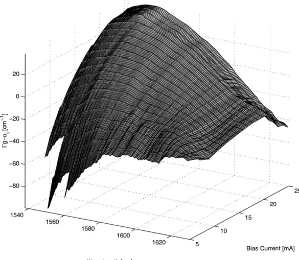
2-12 Overall material gain (Fg - a,) for different biases, E.P.I. growth L = 320pm,
W = 3pm, T = 293.2K . . . . 57
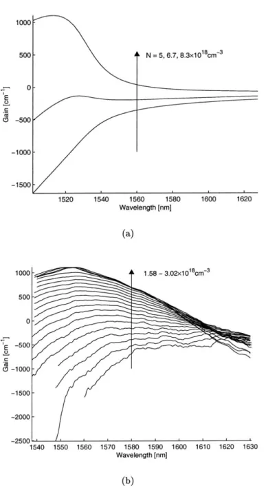
2-13 Gain (g) spectrum from (a) theoretical simulation (b) Hakki-Paoli experimental extraction. E.P.I. growth L = 320pm, W = 3pm. Theory: T = 300K. Experiment:
T = 293.2K . . . . 59
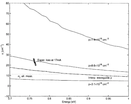
2-14 Theoretical loss curves and experimental loss, E.P.I. growth, L = 320pm, W = 3pm,
T = 293.2K, I = 17mA . . . . 60
2-15 Peak gain (g) versus carrier density (N) for different quantum well temperatures, E .P.I. grow th . . . . 62
2-16 Current Density (J) versus carrier density (N) theory and data, E.P.I. growth. A =1.1x10⁸, B= Ix10-10, T = 293.2K . . . . 63
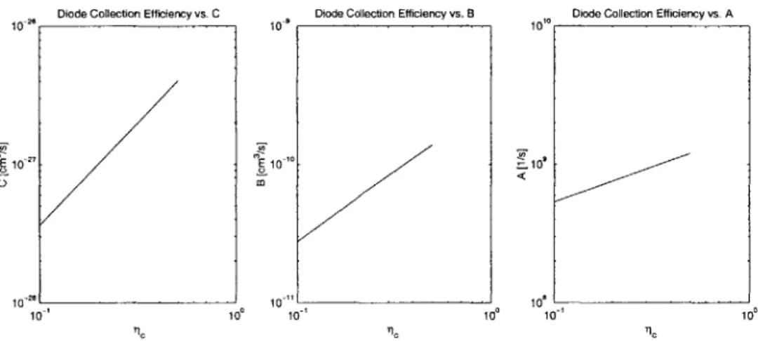
2-17 L-I curve for biases well below threshold along with fitted parameters . . . . 65
2-18 A, B, and C parameters as a function of r,, as fitted to L-I curve . . . . 65
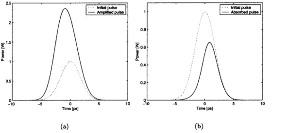
3-1 Examples of (a) gain and (b) absorption saturation effects. Lgain = Lsa = 50pm,
Igain = 4mA, Ysa - -9539cm- 1 . . . . 73
3-2 Example of pulse drifting due to gain saturation; pulse evolves with lighter pulse color. Each pulse represents one round-trip propagation from the previous.
I
= 0follows the propagation at the pulse's group velocity. a = 0, Lgain = 50pm, Igain =
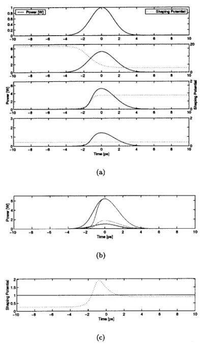
3-3 (a) Pulse evolution with shaping potentials. Each evolved pulse is shown with the shaping potential used to create it from the previous pulse (directly above). Top picture is the original pulse. The following pictures show evolution due to gain
saturation, absorption saturation, and mirror reflection, respectively. (b) Pulses on an absolute scale (pulse evolves with lighter pulse color). (c) Total shaping
potential, including unity line. Lgain = Lsa = 50pm, Igain = 6mA,ga = -1.244 x
104 cm-1,a =
0
. . . . 77 3-4 Self-phase modulation effects due to linewidth enhancement factor. a = 2. Graphsshown are Power (P), Carrier density (N), index (n), instantaneous frequency
(f).
Lgain = Lsa = 50pm, Igain = 4mA, 9,a = -9539cm . . . . 78
3-5 Examples of (a) pulse drifting due to dominant gain saturation in a 2-section pas-sively modelocked laser and (b) pulse drift cancelling in a 2-section active
mode-locked laser. La = Lact = 80pm, Lgain = 3500pm, WM = 2(Lact+L gain) gain
63mA,ga = -1864cm- , IRF = 5mA, gact = -9159cm . . . . . 80
3-6 Gain vs. wavelength at 300K and several carrier densities . . . . 82
3-7 Determination of gp, wo and t2. The fit is second-order. . . . . 82
3-8 Example of pulse broadening due to finite gain bandwidth. (a) shows the input pulse and the broadened pulse. (b) shows the input and broadened spectrum. (c) shows the magnitude of the filter. t2 = 1 x 10 1 3s, gp = 2 x 104cm-1, L = 50pm The gain was increased for illustrative purposes. . . . . 83
3-9 Example of pulse broadening due to dispersion. (a) shows the unchirped input pulse and the broadened pulse. (b) shows the instantaneous frequency. (c) shows the phase of the filter. 02 = 4 x 10- 2 2cm2/s, L = 50pm . . . . 85
3-10 Explanation of split-step method . . . . 92 3-11 Pulse evolution from split-step simulation. Pulse evolves dark to light pulse lines.
Igain = 63mA, g,, = -7776cm- 1. The saturable absorber was split into 4 sections of 20pm each; the gain section was split into 35 sections of 100pm each . . . . . . 93
3-12 Pulse width [(a)&(c)] and pulse energy [(b)&(d)] evolution. (a)&(b) vary the initial pulse energy. (c)&(d) vary the initial pulse width. In all cases, the steady-state pulse width is 4.1ps, pulse energy is 1.lpJ. Laser parameters are the same as in
Figure 3-11. . . . . 95 3-13 Comparison between analytic solution and simulation with (a) gain bandwidth only
(b) dispersion only unchirped Gaussian Pulse input, t2 = O.1ps, 12 = 103ps2 m 1,
L = 1pm, g, = 5 x 104cm-1 (illustrative purposes) . . . . 98
3-14 Diagram of ring cavity [61]. . . . . 99 3-15 Pulse width evolution with various initial pulse widths. Each reach the same steady
state. L = 1 = 50im, go = 4cm-1, ao = 2cm-1, M = 506.6059, wM = 27r x 1GHz, t2 =
5ps
... ... ... 1014-1 Illustration of the state variables in a three-section laser structure with P
sections. The total laser length is PAz. . . . . 111 4-2 Pulse evolution with insufficient broadening forces (infinite gain bandwidth).
Se-lected round trip snapshots are shown. . . . . 115 4-3 Pulse evolution using unstable finite gain bandwidth implementation. (a) the initial
pulse (t = Of s). (b) the pulse at the threshold of instability (t = 58f s). (c) the pulse exhibiting significant instability (t = 63fs). (d) the pulse well beyond the threshold of instability (t = 70fs). . . . . 117 4-4 Parabolic gain spectrum model and the frequency response of filters with varying 'q
(From [31]) . . . . 119 4-5 Fitting of the digital filter parameter, 77, for various At. The fit is to Equation 4.33
for a given t2 = 5 x 10 13s. Shown above are for Az = (a) 1pm (b) 5pm (c) 10pm 124
4-6 Error corresponding to the digital filter approximations defined by the parameters
in Figure 4-5. Shown above are for Az = (a) 1pm (b) 5pm (c) 10pm . . . . 126 4-7 q(gp) for various Az = 1pm, 5pm, 10pm. . . . . 127 4-8 Steady-state pulse width and energy for different space increments. . . . . 132 4-9 Steady-state (a) pulse width and (b) pulse energy for different initial pulse widths. 133
4-10 Steady-state (a) pulse width and (b) pulse energy for different initial pulse energies. 134
4-11 Pulse evolution to steady-state for two different initial relative pulse locations. . . 135
4-12 Laser output with If = 0. The pulse continues to advance in time faster than the group velocity. . . . . 136
4-13 DC L-I curves for three-section laser. . . . . 136
4-14 Optical spectrum of three-section laser. . . . . 138
4-15 Schematic of laser used for design [29]. . . . . 139
4-16 (a) Pulse width and (b) pulse energy versus gain region bias current, for different saturable absorber lengths (no active modulation) . . . . . 142
4-17 (a) Pulse width and (b) pulse energy versus gain region bias current, for different m odulation depths. . . . . 143
4-18 (a) Pulse width and (b) pulse energy versus detuning frequency, for different mod-ulation depths. . . . . 144
4-19 (a) Pulse width and (b) pulse energy versus detuning frequency, for different mod-ulation depths. A more detailed view than Figure 4-18. . . . . 145
4-20 (a) Pulse width and (b) pulse energy versus gain region bias current, for different saturable absorber strengths (measured by carrier lifetime). . . . . 147
4-21 (a) Pulse width and (b) pulse energy versus gain region bias current, for different saturable absorber lengths in a 37.8 GHz cavity. . . . . 149
4-22 (a) Pulse width and (b) pulse energy versus gain region bias current, for different saturable absorber lengths in a 30 GHz cavity. . . . . 149
4-23 (a) Pulse width and (b) pulse energy versus gain region bias current, for different saturable absorber lengths in a 20 GHz cavity. . . . . 150
4-24 (a) Pulse width and (b) pulse energy versus gain region bias current, for different optical loss values. . . . . 151
4-25 (a) Pulse width and (b) pulse energy versus gain region bias current, for different left-hand-side mirror reflectivities. . . . . 152
4-26 (a) Pulse width and (b) pulse energy versus gain region bias current, for different
internal reflections. . . . . 153
3.1 Laser Param eters . . . . 68
4.1 Table of simulation methods. /= suitable application. El = untested but suitable application.
t=
limitations deter usage. suitable otherwise. . . . . 107 4.2 Laser Param eters . . . . 137Introduction
Analog-to-digital converters are an integral technology that allows us to interpret real world
information into electrical data. They are the necessary interface of computers to the
physical world, allowing us to create massive databases, communicate with others across the globe, store and analyze scientific data, and control electrical devices such as robots, to name just a few applications. They also allow us to perform tasks that were never
before possible, such as weather forecast modeling or secure data encryption. The success of computers relies on the ability to transmit, store, and manipulate digital data. Without
this, they would not have been able to achieve the speed, power, and reliability that we take for granted today. The real world, however, is not digital. For example, our limbs
do not have a limited number of specified positions that they can bend. Rather, they can swing freely through a virtually infinite number of positions that span the range of
flexed to extended. If a computer was used to model the movement of a human arm, it would not have the ability to represent the position of the arm to infinite precision since
this would require an infinitely large storage device. It is, however, allowed to take the
infinite number of possible positions and pick (for argument's sake) a large number of them that would suitably represent the entire set. This process is called discretization, and is
similar to rounding a number off to an integral value. The number of discrete values that have been selected to represent the whole analog set determines the accuracy of the digital
representation.
The ability for digital systems to interact with the real world is of great importance. Weather satellites need to translate weather information such as cloud locations,
tempera-ture fluctuations, etc. into digital data in order to transmit this to computers on earth for
analysis. Digital cellular phones take human speech, digitize it, encode it and transmit it via radio waves, which are analog. These wave eventually are received, redigitized, decoded, and played over the listener's phone speaker. Even a computer keyboard takes finger pres-sure and translates this into a digital representation of a letter. All of these applications
necessitate converting analog, real-world data into a digital representation. The devices that perform this action, analog-to-digital (A/D) converters, are the subject of current research.
1.1
A/D Converters
The ability to perform high-speed and/or high-resolution A/D conversion is essential in a
wide variety of applications, such as recording/analysis of scientific data and on-the-fly audio or image data processing. A/D converters take analog signals that are continuous in time
and magnitude, such as human speech or the temperature in a room, and discretize them in both time and magnitude. This is performed in two stages. The continuous-time analog signal is sampled periodically in time, taking only specific values of the waveform (Figure
1-1(b)). Then each of those time-samples are then discretized in magnitude, "rounded" to a specific, discrete magnitude that most closely represents the true value (Figure 1-1(c)). This leads to defining two important figures-of-merit for describing A/D conversion: sampling
rate and sample resolution. The ability to increase the sampling rate, which is typically measured in Hertz (Hz) or samples-per-second, allows more information to be sent in a given
time interval. The increase of the sample resolution, which is measured in bits-per-sample, increases the sensitivity of the information that is collected.
Due to error introduced by noise and quantization, a practical maximum limit is set on the these parameters. In general, the existing state-of-the-art A/D converters follow a trend
7 6 -5 27 - - -.- - - - .. . . . 4-1 - - - -0 > (a) 7- 6-5. 4. 3. 2-1 - 0-(c) 7 6 -. . . . .-. -. . 5 -4 . . .. . . .-. -.. -. -. . - . 0 t (b) 1 bit 2 b -- L>F-bit I bit 0 >V (d)
Figure 1-1: (a) Analog sine wave. (b) Sine wave discretized in time. (c) Sine wave discretized in time and magnitude. (d) Sine wave discretized into binary channels.
...
...- ..
-.
-
...
-.
-..
..
-.
-.
.
... .
-.
-..
the application, a high sampling rate is accompanied by a mediocre resolution, or vice-versa. For example, certain video applications require 14-bits at 2 Megasamples/second (MSPS)
while other audio applications require 24-bits at 96 kilosamples/second [4]. Figure 1-2 shows
a scatter-chart of currently-available A/D converters. Most of these A/D converter systems
are implemented electrically. Since the essentially analog input is typically electrical, this choice makes sense. Electrical systems are inherently high-speed due to electron transport
speeds and lifetimes. The current state-of-the-art converters are primarily implemented with IC transistor technology [4].
22 20 s 18 ---- A- C-S --- ---A Il-VI 16 SApW A AA A 14 -d-o--- sa-.-- -- -AAA 12 --- &1&--4 A-A--4 10 - odulep
hybrid
---1
111l-V IC 2 superc_ __-IE-f4 I E+5 I E+6 i E.1
Sample F
________~1
U A A -* A. A 7 1E+8 1E+9 Rate (Samplesis) IN* 1E+10Figure 1-2: Resolution and sampling rate for currently-existing A/D converters [63]
1.2
Optical A/D Converters
Applications are being developed that require A/D conversion at high speeds and greater
sensitivity. As the need for faster, higher-resolution converters arises, new techniques of
conversion are being explored. The current goal for the next state-of-the-art converters is to create a 10 GHz, 12-bit resolution A/D converter, which is necessary for certain data
col-ope: -1 bit/octave
C 0
lection applications. A/D conversion has traditionally been implemented with all-electrical
components. All-electrical converters are bottlenecked in sampling rate and resolution by electrical sample-and-hold circuitry [59].
In order to overcome the bottleneck, alternative methods of conversion are being
ex-plored. The most promising alternative is to perform optical A/D conversion. Optical A/D conversion is not limited in sampling rate, since it employs optical pulses to bypass the need
for high-speed electrical sample-and-hold circuitry. There is also no cross-talk between the sampling clock (which is optical) and the RF data signal (which is electric).
There are several methods that employ photonics to achieve higher speed and resolu-tion A/D conversion [18, 56]. One of the currently researched methods uses a laser which produces periodic optical pulses. This periodic laser pulse train serves as the sampling
clock for the sampling sub-system. The analog electrical input signal modulates the voltage
input of an electro-optic modulator (EOM), whose optical input is the laser pulse train. As each pulse passes through the EOM, its amplitude is modified by the voltage level of
the electrical input. Thus, the optical input pulses can "read" the radio-frequency (RF) electrical input. The output is an amplitude-modulated train of optical pulses that repre-sent the discretized analog signal. These optical samples are then converted into electrical
step waveforms before they are turned into bits. However, there are still speed limitations
on the electrical components that perform amplitude-digitization. Therefore, the optical-to-electrical sub-system implements a 1:4 time demultiplexer that splits the optical signal into four optical signals that are 1 the data rate of the original (Figure 1-3). 4 These
op-tical samples are then turned into time-discrete electrical step waveforms using an opop-tical detector/integrator (sample-and-hold system) [56]. These lower-frequency electrical signals
can then be digitized by a traditional electrical A/D converter, which converts these
time-discrete electrical waveforms into 12 time-discrete electrical bit waveforms. The bit waveforms are then collected by a computer and then post-processed to multiplex the information into
its original order. This setup has been proposed in [59]. Figure 1-3 shows the diagram of this system. The advantage of this system is by using the demultiplexer, the limitations
of sampling rate of the electrical digitizers can be overcome by splitting the signal into
slower components. By using optical components, limitations of speed and resolution can be LI~bO3Computer 100 do SFDR v D60 Buffer Q--V D6640 and Signl tcInterface muFiber Inu R
Mode-Locked Inunar end Control
Laser
LI1r*D%3 ADb, om4te
samping computer
eong Modulator cairtoanouffer
Oscillator O V ADS644D Interfaceany
1:4 Optical integrate 12 bit
Demultiplexer and Reset 52 MS/s
CFM2 Fig.l 208- MS/s phase-encoded time- demultiplexed optical sampling system conprised of (i)
a fiber ier mode-locked using a resonant tunneling diode (RTD) oscillator, ai a dual-output LiNbOs,
Mach-Zehnder interferometer, (iii) a pair of 1:4 optical time-demultiplexers, (iv) an array of integrate-and-reset circuits, (v) an array of 12-bit quantizers (AD6640) operating at 52 MS/s, and (vi) a computer
for performing control, system calibration, and phase demodulation.
Figure 1-3: Schematic of Proposed Optical A/D system [59]
A quantitative analysis on the maximum achievable resolution for a given sampling frequency leads to a study of the noise present in a practical system and a classification of the different noise phenomenon [63]. In the proposed optical A/D converter, the noise introduces itself at different segments of the system. The first, quantization noise, arises
from the fact that when an analog signal is translated into a discrete magnitude, error from the 'rounding-off' process is created.
Quantization
noise is inherent even in an ideal A/D converter. Other noise sources are non-ideal and contribute to the deviation of the output from the ideal case. This noise can effectively make the lowest significant bits of theratio. The effective usable bits can be calculated, given the SNR:
Neff
= (SNR(dB) - 1.76)/6.02(1.1)
where Neff is the effective number of bits and SNR(dB) is the signal-to-noise ration [dB]. The greatest sources of error come from the noise introduced by the optical pulse train. An ideal pulse train has evenly spaced pulses in time and each equal in magnitude. Optical pulses can have variations in amplitude, which produce variations in the magnitude of the sampled RF signal (Figure 1-4(b)). This is known as amplitude jitter and has a nominal effect on the increase of the system's noise. A more cogent source of error is the variations of time between pulses that cause a non-periodic pulse train (Figure 1-4(c)). This source of error is known as timing jitter and is a parameter for pulse-producing lasers that is not well understood [14, 25, 62, 40].
E .>t t
(a) (b) (c)
Figure 1-4: (a) Ideal pulse train. (b) Pulse train with amplitude jitter. (c) Pulse train with timing jitter.
The maximum achievable bit resolution can be calculated, given a timing jitter, ra:
Be
log
= 2 - 1 (1.2)Btj
=19~
N? /7fs",mpiawhere Bti is the maximum achievable bit rate due to timing jitter limitations and
fsamp
sampling rate of 10 GHz and 12 bits per sample, this would imply a timing jitter of 4.5 fs.
Even for a moderate sampling rate of 1 GHz at 12 bits/sample, a timing jitter of 45 fs is
necessary. Currently, typical semiconductor pulsing lasers have timing jitters of hundreds
of femtoseconds to picoseconds [13], well above that of the necessary specification to realize this high-speed system. Apparently, timing jitter is of utmost concern and remains as the
most important parameter of a pulsed optical source. The challenge lies in creating a laser source that meets the specifications of the proposed system, which necessitates a drastic
decrease in timing jitter.
Several varieties of laser design exist that are capable of producing periodic pulse trains. Examples include gain-switching, Q-switching, and modelocking [58]. Because of jitter, repetition rate, and other concerns, only modelocked lasers have been found as suitable
sources for use in high-speed optical A/D converters (Figure 1-9).
1.3
Modelocking
In a laser, an optical resonator confines the optical field and promotes optical amplification
due to stimulated emission [11]. The resonator confinement is accomplished in one dimen-sion by two partially reflective mirrors that keep the light within the laser cavity. A fraction of that light is transmitted through the mirrors; this light that escapes is the observed
out-put of a laser. In a simple laser design, these mirrors create Fabry-Perot resonances of the optical electro-magnetic field when a lasing steady-state is reached. A 1-dimensional resonant cavity can theoretically support a countably infinite number of these Fabry-Perot
resonances (see Section 2.4.2). This produces a frequency comb where the resonance peaks, called modes, are separated by the round-trip frequency of the Fabry-Perot cavity
(Fig-ure 1-5(a)).
Due to the laser's active region's gain bandwidth, only one or a few of these modes exist
in an above-threshold laser steady-state condition. Typically, the phase of these modes are uncorrelated. This produces a laser output that is randomly distributed in time but
modes are locked together so that they do not drift with respect to each other (or at most drift lineary, causing a time drift to the entire pulse), then the output of the light becomes a pulse train. A simple explanation for this is that the inverse Fourier transform of an infinite
train of evenly-spaced frequency impulses is an infinite train of evenly-spaced impulses in the time-domain. These time-domain spikes correspond to optical pulses. Due to the finite
gain bandwidth of the laser, only a finite number of frequency-domain peaks are available. This corresponds to a non-ideal impulse in the time-domain, i.e. an optical pulse with a
finite, non-zero pulse width (Figure 1-5(b)). Since the Fabry-Perot resonance frequencies of the different modes are integral multiples of the round-trip frequency of the cavity, the pulse train exists at a mode separation at the round-trip frequency of the cavity also. Hence, the laser is modelocked and the output is an optical pulse train at the round-trip time of the Fabry-Perot cavity.
(b
(a) (b)
Figure 1-5: (a) Frequency-domain and (b) Time-domain representations of modelocked pulses
Modelocked lasers have the best chance of producing pulses that can meet the
specifi-cations to build the proposed A/D converter system. Prior results from this class of lasers promises the closest specifications in jitter and repetition rate to the proposed system. The repetition rate of modelocked lasers are determined by the round-trip frequency (or some
harmonic) of the laser resonator. Modelocked lasers have exhibited repetition rates of over 100 GHz [22J, well beyond the specifications of the proposed system. Since the phases of the modes are correlated, the time variation between pulses is reduced. Actively mode-locked lasers have exhibited timing jitter values as low as 50 - 100fs [33, 6, 15], whereas
gain-switched lasers have timing jitter values typically greater than 1 ps [17, 40].
Modelocking has been achieved in a variety of material systems and configurations.
Solid-state crystal modelocked lasers were the first demonstrated modelocked lasers. They utilize a solid-state crystal active element and typically employ free-space optics to define a
resonant cavity. They provide high-power, short pulse width, low jitter pulses [19], however they are not usable in practical, high-volume applications due to their cost and size. Another
currently researched method is fiber ring laser modelocking. Fiber ring lasers employ lengths of Erbium-doped fiber to provide a cost-effective gain-medium waveguide that can be looped
into a ring configuration. Free-space optics are placed in the path of the ring geometry to produce modelocking. Fiber ring lasers are excellent choices for a modelocking, providing
reasonably low jitter and smaller size than their solid-state crystal counterparts, but they
continue to demand a relatively large volume due to the fiber lengths and optics [26].
The method explored in this thesis is semiconductor diode laser modelocking. Tradition-ally, semiconductor laser modelocking was performed by using semiconductor modelocking segments coupled together through free-space optics [16]. The facet reflectivity of the seg-ments is kept to a minimum by anti-reflection coating and the light is typically focused
through lenses. While typically smaller in real-estate than the other modelocking methods, the use of bulk optics necessitates sizable area constraints. However, the field of integrated
circuits provides the ability to monolithicly integrate all necessary modelocking components onto a single semiconductor wafer. Typical dimensions for a monolithic semiconductor
modelocked laser wafer are less than a square millimeter and a few hundred microns thick. Fabrication techniques allow for massive parallel manufacturing, yielding low-cost,
high-performance modelocked laser sources. The drawbacks are lower pulse power, and slightly higher timing jitter than their fiber ring laser counterparts.
The two major classifications of modelocking are active and passive modelocking. They are presented below in the context of semiconductor modelocked lasers but are general for
all modelocked devices.
1.3.1 Active Modelocking
A general active modelocking scheme is shown in Figure 1-6. It consists of two major sections: (a) an active modulation section that is modulated by an RF signal at the
round-trip frequency of the cavity and (b) a waveguide section that provides a cavity for the pulses to propagate through. The RF signal is typically a sinusoid but can be any sharply peaked function of current. This current modulation produces a carrier density modulation which in turn produces a photon gain modulation within the active section. Given an existing
pulse within this cavity, it will enter the active section at the round-trip frequency of the cavity. If it has modelocked, then the pulse should propagate through the active section
while the photon gain within that section is at its peak. When the pulse is not present in the cavity, the gain should be lower than the peak, until the pulse returns again to the active
section. This time-dependent gain function causes the photon field to be highest only when the gain is highest, thus producing a pulse that propagates at the round-trip frequency of
the cavity.
Rather than a time-domain explanation, a frequency-domain explanation can be used
to explain this modelocking phenomenon. A frequency comb exists due to the Fabry-Perot resonances of the cavity. Each frequency mode is separated by the round-trip frequency
of the cavity, but the time-domain profile is random due to the uncorrelated phases of the Fabry-Perot modes. The RF modulation, being at the round-trip frequency of the cavity, causes a non-linear coupling between the Fabry-Perot modes of the laser cavity, allowing energy from each mode to couple into their neighboring modes. This energy coupling also
implies a phase coupling, since the photons carry with them their phase. Eventually, a
steady-state solution of this mode coupling is a total homogeneity of phase. The phase locking implies the time-domain profile of the photon field (which is the inverse Fourier
transform of the frequency mode train) is a pulse train.
1.3.2 Passive Modelocking
Passive modelocking again requires at least two major segments, as shown in Figure 1-8: (a) a saturable absorber section and (b) a gain section. The purpose of the saturable absorber
section, given a pulse propagating through it, is to attenuate the pulse, thus shortening its
pulse width. Because of loss saturation in the saturable absorber, there will be a non-linear attenuation of the pulse. As the pulse enters the absorber, the front end of the pulse is
attenuated as photons are absorbed by the material and excite electrons into the conduction band. As more and more of the pulse propagates through the absorber region, more of it is absorbed and the carrier density rises. This results in a reduction of the loss of the
section, since there are fewer excitable valence electrons. If there is sufficient energy within the pulse, this will cause the material to approach transparency, which is the state of no
loss or gain (the absorption is saturated). Hence, the end result is the pulse's leading edge
is attenuated while the trailing edge is not. This effectively results in "shaving off' the front edge of the pulse and shortening the pulse width. If the gain is also saturable, the opposite effect occurs as the pulse propagates within the gain section. The leading edge
of the pulse will be amplified while the trailing edge will not as much, thus resulting in a widening of the pulse. In a passively-modelocked laser, the competition of the saturable absorber's pulse narrowing and the gain section's pulse broadening leads to a steady-state round-trip condition in which the pulse propagates through the laser and returns to its
original position and direction in exactly the same shape. The pulse has effectively been
narrowed, broadened, broadened again, and narrowed back to its original shape.
Active modelocking is useful when low jitter pulses are desired. This is due to the
fact that the RF modulation source serves also as a stabilizer of pulse period. The RF source, while inherently noisy itself, stabilizes the pulse period more effectively than without
the source. Passive modelocking has no such stabilizing source and therefore has much higher timing jitter. Passive modelocking, however, is not limited in repetition rate by the
I I
0
V(t)=Vosin(fot)
Mirror
2L*-=fon
Lfo
2fo 3fo 4fo
f
fo
0
fo
f
Figure 1-6: General active modelocking scheme: (a) active section (b) waveguide section. Energy is coupled from each mode to its neighbors.
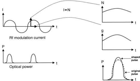
N 1+N t Rf modulation current Optical power 9 St shaped P ' pulse A L I ' original pulse -It
Figure 1-7: Time domain explanation of active modelocking. The photon gain is highest when the pulse inhabits the RF Gain region.
L
Mirror
A1
163k
P-
-
-tm
Mirror
Mirror
Round-trip pulse evolution
- J. %
sorber +-+- Gai
Dotted: steady-state pulse profile, Solid: evolved pulse profile
Figure 1-8: General passive modelocking scheme: (a) saturable absorber section (b) gain section
maximum obtainable RF source frequency, which typically cannot rise above 50 GHz. Since
a source is not needed, the upper-bound on the repetition rate is not bottlenecked by this.
Rather, the repetition rate is defined solely by the length of the laser, since this determines the round-trip frequency of the laser. Practically, there is a maximum repetition rate that
is imposed by absorber to gain ratios [39].
1.3.3 Hybrid Modelocking
It is not a large step forward to realize a system that utilizies both active and passive modelocking phenomena. A three-section device can be fabricated to provide an actively
modulated section, a saturable absorption section, as well as a gain/waveguide section. This
technique is known as hybrid modelocking [16] and it provides the benefits as well as deficits
of both methods of modelocking. Typical figures of merit for the three laser designs are
shown in Figure 1-9.
Modelocked lasers can be used for applications other than optical A/D conversion. It k
TABLE I
COMPAvs Ow OF M tIssOMENT SyatjCums PEtAO*MANCF
Spectral Time- Pulse Repetition
Cavity Modulation Pulse width Width Bandwidth Energy Rate Wavelength Active
Type Technique (ps) (GHZ) Product (p.) (OHz) (0m) Region Rference Ext. Active 1.4 342 0.48 0.28 3 1I3 Bulk 171
Two-Seg.
Ext. Passive 2.5 720 1.8 0.7 5 0.84 4 QW 1221
Two-Seg.
Ext. Hybrid 2.5 1000 2.5 0.8 5 0.84 4 QW 1221
Two-Seg.
Ext. Hybrid 1.9 900 1.71 0.18 6 0.83 Bulk (16), (271
Thee-Seg. Mon, Active 13 330 4,3 0.19 5.5 0184 4 QW (22) Two-Seg. Mon. Hybrid 6.5 540 3.5 0.13 5.5 0,4 4 QW 1221 ThrccSeg. MOn. Passive 10 400 4.0 0.25 5.5 0.84 4 QW 122) Two-Seg. Mon. Passive 5.5 550 3.0 0.53 I1 0.84 4 QW Two-Seg. Mon. Hybrid 2.2 500 1.1 0.03 21 1.58 4 QW Three-Seg. Mon. Passive 1.3 600 0,78 0.02 41 1.58 4QW (381 Two-Seg.
Mon. aSwitch 15 2400 36 4 1 0.825 Bulk Two-Seg.
Mon, Gain-Switch 13 4000 52 3.4 0.822 Bulk TwoSg.
Figure 1-9: Semiconductor modelocked laser comparison [17]
is used for performing pump-probe experiments for exploring carrier dynamics. A "pump" pulse excites the sample of interest in which a "probe" pulse follows after some time delay
and is detected. The detection of the probe pulse tells how the material has been affected
by the pump pulse and the time delay between pulses. It is a useful technique for measuring carrier lifetimes.
1.4
Thesis Overview
This thesis concentrates on the development of modelocked semiconductor lasers that will
eventually be used in an A/D converter system. Modelocked lasers exhibit the lowest jitter
of optical pulse sources and can produce pulses faster than 100 GHz [9, 3]. This thesis will
study the dynamics of modelocked laser diodes (MLLD) in order to improve performance and optimize design.
of modelocking. Chapter 2 goes into the various experimental and theoretical methods of physical laser characterization. Chapter 3 critically analyzes the split-step Fourier method
and discusses its limitations. Chapter 4 presents the split-step finite difference (SSFD)
method and uses the method to derive trends for design purposes. Chapter 5 summarizes the works presented in this thesis.
Characterization
In order to better understand the characteristics and quality of a laser design, one must
analyze the various parameters that determine the performance of the laser. For example, knowing the DC lasing threshold is important to understanding where to bias a laser when
modelocking (See Chapters 3 and 4). These laser parameters can be derived through theory or determined experimentally. A careful choice of which method to use for each parameter
is important. Certain parameters are easily determinable through experiment, and their results can typically be more accurate than a theoretical value. However, others are difficult
to impossible to determine through experiment and a theoretical approach is necessary. This chapter first discusses the design of the lasers used in this thesis. It then introduces the
various laser parameters and provides several approaches to determining them. A discussion of sources of error and the accuracy of each approach follows most techniques.
2.1
Laser Design
The laser used in all modelocked experiments is a 1550 nm Fabry-Perot quantum well laser
designed and processed by Farhan Rana at MIT and grown by Patrick Abraham at the
University of California, Santa Barbara. The substrate is 3 - 5 x 10 1 7cm-3 S-doped n-type InP (uncertainty due to growth calibration). The six quantum wells are 70A thick 1.55pm
InGaAsP with +1% strain. The barriers are 70A thick 1.18pm InGaAsP with no strain.
The ridge layer is 5x10¹⁸C- 3 Zn-doped p-type InP and is 1.5pm thick. Ridge widths were processed in 1.5 and 2.0pm widths. Figure 2-1 shows the hybrid modelocked laser profile, including the biasing scheme, and band structure.
The laser is current- and index-guided by etching a ridge (1.5pm and 2.Opm widths) through the p-type InP down to but not including the active region. A very thin layer of
oxide is then deposited on the entire top of the wafer. The oxide allows a layer of polyimide to be deposited. The polyimide is spun on and cured. The entire wafer surface is then
planarized to the height of the ridge surface. Ohmic contacts are then deposited on the ridge surface and entire wafer backside.
All subsections of the modelocked laser, including active region, passive region, and gain region are integrated onto a single wafer. The three sections were electrically isolated by
etching two 1pm wide channels through the transverse direction of the ridge (see Figure 2-2). The etching of these two channels was included in the same step as the etching of the
ridge itself, therefore the channels extend down to the active region. During the polyimide
spinning step, polyimide was able to fill the channel to provide a planar surface for the met-allization. The ohmic contacts were deposited over the ridge areas, excluding the channels. The inter-section resistance was measured to be greater than
1MQ.
An additional growth was prepared by E.P.I., a foundry in England. This laser design
was used primarily in the characterization techniques found in this chapter. The major
differences are the number and size of the quantum wells and the ridge dimensions. The bottom n-doped region was doped at 3 - 5x 10 17cm-3. Five 60A quantum wells with +0.8% strain were separated by 100A barriers with -0.5% strain. The separate confinement heterostructure (SCH) layers were 120nm thick; both n- and p-type layers were doped 1x 10 17cm-3. Both the SCH and barriers were 1.3pLm InGaAsP. The p-type ridge was doped 5x 10 17cm-3 and was 1.5pm thick and several different widths were processed, including 3, 4, and 5pm. Figure 2-3 shows the band structure of this alternate laser design.
center gain section passive saturable absorber section 1p m gap OVD
[too-I
I
(a) cladding: 1ooA 1.3ptop of laser a) L 1 undoped 1.55pm InGaAsP Ex
U1
"aCD0. 0 V. Vwells 70A
strain +0.8%
barriers 90A
strain -0.5%
(b)Figure 2-1: (a) Side view of laser, including biasing scheme. (b) Band structure of active region.
active section VAC CO CO, a-CoL 00$" I I
active section - MQW active layer p-InP ridge (a) active section Ohmic contact MQW active layer Ohmic contact p-InP ridge (b)
Figure 2-2: Schematic of hybrid laser design: (a) without (shown for detail) and (b) with polyimide planarization.
. top of laser
InGaAsP
wells, barriers
and cladding
... C> undoped E. 1.55pm InGaAsP 0-*n C LO N C5 wells, 60A barriers 1
OOA
strain +0.8% strain -0.5%
Figure 2-3: E.P.I. laser design
2.2
Laser Rate Equations
A basic but powerful model for continuous wave (CW) laser operation describes the time rate of change of the carrier concentration and photon concentration [11]. These equations
are: dN _ iI N
dt
-qV - - - vggNp (2.1) dt qV T, dN p= _N~ 22 FvggNf+ spRsp - (2.2)dt
T,where N is the carrier concentration [cm 3], t is time [s], qj is the internal quantum
effi-ciency, I is current [A], q is the fundamental electron charge [C], V is voltage [V],
mc
is the carrier lifetime [s], V. is the photon group velocity [m/s], g is the differential gain [cm-1 , Np is the photon density [cm- 3], F is the photon confinement factor,f,3
is the spontaneous emission factor, Rs, is the rate of spontaneous emission [cm--3s-1], and Tp is the photonlifetime [s]. The carrier lifetime, T, and the photon lifetime, Tp, are abbreviations for: N -AN+BN2 + CN3 (2.3) Tc 1 - = v (a + am) (2.4)
where for low carrier concentrations, A is the trap recombination coefficient [s- 1], B is the
bimolecular recombination coefficient [cm-3s1 J (accounts for spontaneous emission), C is
the Auger recombination coefficient [cm~6
s- 1] (see Section 2.4.6 for explanation at high
carrier concentrations), ai is the internal loss [cm-1] (due to material loss), and am is the distributed mirror loss [cm-1. It is important to note that the recombination coefficients
in the carrier lifetime equation only take on these definitions under low carrier densities
when Boltzmann statistics hold. Under high carrier densities, the Fermi statistics of the electron occupancy take on more complicated dependencies rather than a simple
integral-degree polynomial expansion. Section 2.4.6 explains this in further detail. The internal loss is due to heavy-hole to light-hole intervalence band absorption. This is a function of carrier
density and photon energy, and will be described in the next section. The mirror loss, am, is due to the coupling of photon energy out of the two mirror facets, but the definition distributes this loss over the length of the cavity. It is defined as:
1 1
am = - In (2.5)
L R
where L is the Fabry-Perot cavity length [cm] and R is the power reflectivity of the end mirror facets. The spontaneous emission rate, Rap, comes from Equation 2.3 and for low
carrier densities takes the form:
Under high carrier densities, R8p has a weaker carrier density dependence as explained in
Section 2.4.6.
Finally, an optical power output equation can be derived for current values above
thresh-old:
P = r a( (I - hh) x - (2.7)
ai + am q 2
where h is Planck's constant [J-s] and v is the fundamental lasing wavelength. The subscript
"th" is used to represent the variable value at the threshold condition. Thus, Ith represents
the current needed to reach the threshold condition. Frequently, we define:
7
1d -Mm (2.8)
ai + am 2
where rid is known as the differential quantum efficiency. Since spontaneous emission
dom-inates for sub-threshold regimes, a power/facet equation below threshold can be derived:
Psp= ci70ir ---I (2.9)
q
where r, is the radiative efficiency and r is the collection efficiency. r7r is the fraction of carrier recombination that is accounted for by spontaneous emission:
Rs
~
(2.10)Ir (N/Ir,
A brief explanation of each term in Equations 2.1 and 2.2 are as follows. In the carrier rate equation, the first term on the right-hand side accounts for carrier injection into the
active region from a current source. The second term accounts for carrier relaxation due to interactions in the semiconductor. The third term accounts for carrier recombination due
to stimulated emission from the lasing modes. In the photon rate equation, the first term
on the right-hand side accounts for the photon creation rate due to stimulated emission into the lasing mode. The second term accounts for spontaneous emission coupling into
the lasing mode. The third term accounts for photon absorption losses due to interactions with the semiconductor. Further information on the laser rate equations can be found in
Chapter 2 of [11].
It is important to characterize these laser parameters to better understand the quality of its design and help explain its performance. The remainder of this chapter is devoted to the determination of the parameters which are found in the laser rate equations and their
supplemental equations.
2.3
Theoretically-Derived Parameters
2.3.1 Group Velocity (v9)
The photon group velocity represents the speed at which photon energy propagates. In terms of laser pulses, this is the velocity of the pulse as it propagates within the
semi-conductor. This is different from phase velocity, which is the speed at which the carrier frequency (in this case, the frequency that corresponds to a 1550nm free-space wavelength)
propagates. The group velocity is determined by knowing the group index of the material. Since the laser is heterogeneous, the index is spatially dependent. The group index is found by determining the photon field profile within the laser cavity and performing a weighted average of the different indexes by the percentage photon density of each section. Since the
index is wavelength dependent (due to material dispersion effects), the group velocity, vg,
will be also:
C
Vg = (2.11)
ng
where ng is the group velocity. Since the wavelengths within the linewidth of a laser typically
span a short range, the group velocity can usually be approximated as constant. A method to determine group index is explained in Section 2.4.4.
2.3.2
Confinement Factor (F)
The confinement factor, F, represents the percentage of the steady-state photon energy that lies in the active region of the semiconductor. In a Fabry-Perot laser, the photon field propagates along the axial direction (the axis as defined in the direction of the laser ridge, or z-axis, as conventionally defined). The active region is defined as the region in the laser that stimulated emission occurs. This will be within the quantum wells, since they provide electron and hole confinement. Since the active region extends the entire axial length as well as the entire plane of the laser, the confinement of the laser field in these two directions is 100%. The quantum wells, however, only cover a small portion of the vertical direction and therefore the photon field extends well beyond them. The confinement factor can be determined theoretically by knowing the structure dimensions and solving for the steady-state photon field as confined by the cladding and quantum wells. This is accomplished by performing a 2-dimensional solution of the photon field within the cavity. Once the field profile is determined, the percentage of the photon field that lies within the multiple quantum wells is added up, which becomes the confinement factor. This simulation was written by Farhan Rana. Figure 2-4 shows this solution for the laser under study. Using the 2-D solver, F = 0.00918 for each of the quantum wells in the E.P.I. laser. Summing up the total confinement factor for all five quantum wells yields a total F = 0.0459.
2.3.3
Mirror Reflectivity (R)
The mirror reflectivity can be determined simply by knowing the group index of the photon field within the semiconductor, as well as the index outside the cavity. A simple boundary condition solution gives the transmission and reflection through a mirror facet.
ni
- n2r n(2.12)=
22 (2.13)
![Figure 1-2: Resolution and sampling rate for currently-existing A/D converters [63]](https://thumb-eu.123doks.com/thumbv2/123doknet/13954286.452493/20.918.210.749.441.763/figure-resolution-sampling-rate-currently-existing-d-converters.webp)