HAL Id: hal-02873051
https://hal.archives-ouvertes.fr/hal-02873051
Preprint submitted on 18 Jun 2020
HAL is a multi-disciplinary open access
archive for the deposit and dissemination of
sci-entific research documents, whether they are
pub-lished or not. The documents may come from
teaching and research institutions in France or
abroad, or from public or private research centers.
L’archive ouverte pluridisciplinaire HAL, est
destinée au dépôt et à la diffusion de documents
scientifiques de niveau recherche, publiés ou non,
émanant des établissements d’enseignement et de
recherche français ou étrangers, des laboratoires
publics ou privés.
Direct bonding and debonding approach of ultrathin
glass substrates for high temperature devices
Messaoud Bedjaoui, Sylvain Poulet
To cite this version:
Messaoud Bedjaoui, Sylvain Poulet. Direct bonding and debonding approach of ultrathin glass
sub-strates for high temperature devices. 2020. �hal-02873051�
Direct bonding and debonding approach of ultrathin glass substrates for high
temperature devices
Messaoud Bedjaoui
Univ. Grenoble Alpes, F-38000 Grenoble, France CEA, LETI, Minatec Campus,
F-38054-Grenoble, France messaoud.bedjaoui@cea.fr
Sylvain Poulet
Univ. Grenoble Alpes, F-38000 Grenoble, France CEA, LETI, Minatec Campus,
38054-Grenoble, France sylvain.poulet@cea.fr
Abstract—The advent of flexible thin-film electronic devices on
ultrathin substrates is driven by the need to develop alternative handling methods fully compatible with front-end and back-end processes. The purpose of this work is to present a new handling approach for ultrathin glass substrates based on direct glass-glass bonding and peel-off debonding at room temperature. This concept is evaluated through the realization of thin-film batteries (<20µm) on ultrathin glass substrates (<100µm). In order to bond, the ultrathin glass is laminated on thick carrier glass (>500µm) without intermediate layer. The stack of thin film battery is fabricated using sequential physical vapor depositions at temperature values up to 400°C. The debond process is completed at room temperature by mechanical peel-off of the encapsulation film laminated on thin film battery. As the results, there is no sign of any crack of the ultrathin glass (<100µm) after debonding. Furthermore, the Electrochemical Impedance Spectroscopy (EIS) and galvanostatic cycling carried out before and after debonding process reveal that the device performances are slightly stable.
Keywords-Ultrathin glass; Handling, Bonding process, Debonding technique; Thin film batteries
I. INTRODUCTION
In the large flexible electronic market, there is an increasing need to develop ultrathin film device on thinner and non-silicon based substrates. This is especially the case for many applications including optoelectronics (e.g. LCD displays), lighting (e.g. OLED displays), photovoltaics (e.g. solar cells), biotechnology (e.g. microfluidic devices) and micro power modules (e.g. lithium microbatteries). As such, glass is a perfect substrate material for microelectronic and medical device applications [1], [2] because of its high insulation and excellent chemical, mechanical and optical properties. Furthermore, the appearance of thin flex glass material in the market, such as G-LeafTM (Nippon Electric Glass), AF32® Eco Thin Glass (Schott AG), and Willow® Glass (Corning), have generated significant interest as a flexible packaging and substrate material. This glass is produced by a down-draw method that enables production of glass plates in a thickness up to 25 µm as a large scale either in sheet-to-sheet or roll-to-roll processing. However, the fabrication of thin film devices on ultrathin glass substrates faces the critical mechanical fragility of ultrathin glass. More specifically, the accurate handling of these substrates is a
technical and practical challenge in the fabrication process including the substrate transfer steps and different layer deposition at high temperature range (300-650°C).
In current practice, the widely accepted method of thin wafer handling is to attach a thick and rigid carrier to a device wafer with temporary bonding adhesive. The carrier is either silicon or glass, and is used to support the product wafer up to 300 mm diameter through processes including wafer grinding, plasma or wet etching, chemical mechanical planarization, and other processing, depending on use. These methods involve the use of suitable temporary adhesive compatible with a number of important requirements [3]. Among them, the adhesive must be unaffected by temperature process, easily removed at room temperature, must adhere to a variety of semiconductor substrates, metals and dielectrics and chemically resistant to a wide range of semiconductor chemicals (solvents, acids and cleaning solutions). Finally, it must have a very short time and gentle debonding process without imparting damage to the thinned wafer or the features of its active components. There are several options for debonding of thin wafers from the organic temporary glues [4], [5], [6]: mechanical separation, ultraviolet (UV) or heat curing and release, thermal sliding-off, chemical activation or solvent swelling and laser activation with UV or infrared (IR) sources.
This state of the art process was studied intensively over the last years, but the common downside of the developed organic adhesives was the thermal instability at temperature above 300°C, making the temporary bonding approach incompatible with more applications, like Liquid Crystals (LC) displays, Thin Film Transistor (TFT) and Thin Film Batteries (TFB). For instance, the active layers of TFB including current collectors, electrodes and electrolyte are usually fabricated using physical vapor deposition (PVD) techniques at high temperature (300°C-650°C) [7]. Most importantly, such components normally requires the use of ultra-performed packaging due to its high sensitivity in contact with external air. Furthermore, the increased degree of fragility becomes more pronounced because of the mechanical properties of the active materials fabricated on ultra-thin glass substrates. For these reasons, a reliable
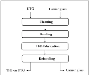
Cleaning
Bonding
TFB fabrication
Debonding UTG Carrier glass
TFB on UTG Carrier glass
handling technique of ultra-thin glass substrates play a critical role in the high-yield and low-cost fabrication of ultrathin devices enabling handling through production processes.
The purpose of this study is to introduce a new cost reduction concept of handling for ultrathin glass substrates covering both bonding and debonding processes. This concept is evaluated through the realization of thin-film batteries (<20µm) on ultrathin alkali-free glass substrates UTG (<100µm) directly bonded on rigid and thick glass carrier (>500µm) without intermediate layer. In the direct bonding process, the bonding surfaces are attached using the contact force at room temperature. The encapsulation of TFB layers fabricated on the UTG topside is provided by the lamination of thinner and flexible barrier films using Pressure Sensitive Adhesive (PSA) techniques. Advantageously, the approach proposed in this work exploit the encapsulation film for the benefit of UTG debonding using mechanical peel-off. The work described in this paper aimed to achieve debonding of wafer device at room temperature with low-stress process that utilizes no chemicals. This paper covers two elementary parts: (i) temporary bonding of UTG substrates onto a carrier glass and debonding after completion of the entire TFB process; (ii) Experimental feasibility of TFB technology on ultra-thin glass substrates. The general performances of TFB after fabrication on bonded UTG substrates and under peeling-off process are evaluated and compared using electrochemical techniques based on Electrochemical Impedance Spectroscopy (EIS) and galvanostatic cycling analysis.
II. EXPERIMENTAL APPROACH
A. Materials
In this paper, we exclusively employed the AF32 alkaline-free borosilicate glass manufactured by Schott as UTG substrate as well as carrier glass. However, our experiments can be extended to similar glass provided by other suppliers (Corning, NEG, AGC, etc.). These kinds of glass are not compatible with conventional anodic wafer bonding methods because of their particular chemical composition (sodium poor glasses). Experimentally, substrate materials with relatively high transformation temperature (typically Tg>500°C) are highly desired for the fabrication for a broad range of devices, such as Thin Film Batteries. On the other hand, Coefficient of Thermal Expansion (CTE) matching of UTG substrate and glass carrier materials is a critical factor for the achievement of direct bonding approach. Indeed, it is extremely important to ensure high thermal and mechanical stability of the bonding interface over the ranges of TFB fabrication conditions. This enables the bonded UTG to successfully survive the TFB production steps. The most important characteristics of the UTG substrates and glass carrier which form the bonded assembly used in this work are shown in table 1.
TABLE I. GENERAL CHARACTERISTICS OF EMPLOYED UTG AND CARRIER GLASS
UTG Glass carrier
Thikness 100µm, 50µm 500µm, 700µm Dimension 8” wafer, A6 plate 8” wafer, A6 plate Transformation temperature Tg 700-750°C 700-750°C Coeficient of Thermal Expansion CTE (0 to 300°C) 3-5 ppm/°C 3-5 ppm/°C B. Bonding process
The main fabrication steps for the approach proposed in this work are outlined in Fig.1. Prior to bonding, the surfaces of glass samples were gently cleaned using detergent, lens tissues and ultrasonic baths followed by DI water rinsing and compressed air drying in order to remove any contamination and dust. The root mean square (RMS) of roughness (Rq) (images not shown here) measured on the UTG and glass carrier surfaces ranges from 0.15 to 0.2 nm. These values are highly desirable for the success of glass to glass bonding.
The direct bonding is performed at room temperature under ambient atmosphere using rigid glass carrier to provide sufficient mechanical support of the ultrathin glass without using of intermediate adhesive agents or polymer bonding materials. The alignment and the contact force between the UTG and the corresponding carrier glass are programmed using a dedicated lamination tool (pressure of 0.5 x10⁶ Pa, speed of 40 mm.s-1). For practical convenience, the size of the carrier glass needs to be carefully considered. Thus, the typical choices are a carrier that is equal to or slightly greater in diameter to the UTG. In our case, the carrier glass size is generally chosen to have 1 to 5 mm as lateral margin in comparison to UTG sheet.
Figure 1. Process flow of direct bonding and debondig approach for thin film batteries.
Pulling head
Advanced force gauge
Fixation recess
Displacement control Sample mounting stage
Mounting bracket Encapsulation film UTG Glass carrier Grips Pulling direction Non-encapsulated TFB Barrier film Encapsulated TFB’s Carrier glass Bonded UTG substrate Figure 2. Illustration of the bond strength measurement set-up. The inset
photgraph shows a 50µm UTG under peeling from 700µm glass carrier.
For bonding strength measurements, the bonded assemblies were firmly fixed on a host stage by placing the glass carrier at the stage fixation recess with mounting brackets. The UTG bond strength was investigated using a force test motorized system, Multitest 2.5-d (Mecmesin) shown in Fig.2. An advanced force gauge (AFG) of 50N was used to measure the bond strength of the UTG substrate during peeling. It was attached to a corner of the encapsulation film and pulled upwards with a pulling speed of 5 mm.min-1, thereby exerting a pull force on the attached UTG substrate as illustrated in the inset of Fig.2.
C. TFB fabrication
Once the UTG and the carrier glass have been bonded, thin film lithium batteries can be deposited on the top side of ultrathin glass substrate. Based on vacuum physical vapor deposition, the full stack of thin film battery is fabricated by shadow masking techniques using an ENDURA sputtering platform (Applied Materials) connected to an argon-filled glove box. In this tool, the sandwich formed by the bonded UTG on glass carrier and the clamped shadow mask is transported from one deposit chamber to another through a transfer chamber using a mechanical robot. Before deposition, a vacuum was created into each chamber until the pressure was less than 4 × 10⁻⁶ Pa. In the present work, the anodic and cathodic current collectors (250 nm) are deposited from titanium target under 100% argon atmosphere at room temperature with an incident power density of 24 W.cm-2. Titanium oxysulfide (TiOS) and metallic lithium were selected as the active materials for the cathode and anode, respectively. Prior to
each deposition, a pre-sputtering was systematically carried out for 20 min. The thick 2 µm TiOS cathode was sputtered in DC mode with a titanium target. A working density power of 2.6 W.cm-2 and a temperature of 180°C were applied to the target under an argon/oxygen (1%) atmosphere with a constant gas flow of 50 sccm and a constant hydrogen sulfide flow rate of 60 sccm. Another embodiment concerns the employment of Lithium cobalt oxide (LCO) as cathode. The latter requires annealing at high temperature range (400°C-650°C) for few hours to get the performing crystalline structure. For the all-solid-state microbattery architecture, the two electrodes are separated by a lithium phosphorus oxynitride (LiPON) electrolyte, which enable ion transfer between the two electrodes. Here, a 1.5µm thick LiPON is deposited by radiofrequency reactive sputtering at a power density of 1.7 W.cm-2 using a (Li2O-Li3PO4-B2O5)
target in pure nitrogen atmosphere. Using these conditions, the temperature ranges from 300°C to 350°C during the LiPONB deposit (90 min). To complete the TFB stack, metallic lithium is deposited in a thermal evaporation chamber with a growth rate of 150 nm. min−1. During this step, the temperature process can easily reach 100°C.
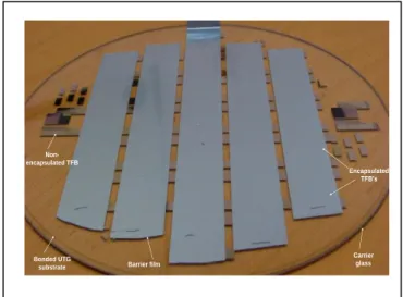
For battery technology, it is commonly admitted that lithium layer is highly sensitive to atmosphere elements, including moisture and oxygen [8]. The requirements for protecting TFB expressed as Water Vapor Transmission Rate (WVTR) range from 10-4 g.m-2.j-1 to less than 10-5 g.m-2.j-1. This barrier requirement can be achieved by the lamination of 50 µm thick bilayer structure (polymer/metal) using PSA (Pressure Sensitive Adhesive) techniques. In this work, the encapsulation step is carried out using barrier band in an argon glove box with roll laminator at a temperature of 80°C and a maximum pressure of 2x10⁵ Pa. Based on the above steps, Fig. 3 shows a set of TFB realized on 8” UTG wafer (AF32, 100µm) bonded on glass carrier (AF32, 500µm).
Figure 3. Photograph showing thin film batteries deposited on 8” wafer obtained by bonding 100µm UTG on 500µm glass carrier.
Peeling force Glass carrier UTG substrate Encapsulation film TFB (a) UTG limit carrier limit 20 mm (b) UTG limit 20 mm D. Debonding process
The purpose of debonding process is to separate the device wafer from the rigid carrier substrate after completion of the entire TFB fabrication. The approach proposed in this work is completed by mechanical peel-off at room temperature of the sandwich formed by the barrier film, thin film battery and ultrathin glass from rigid glass carrier. As shown in Fig.4, encapsulation film is used to peel the TFB deposited on UTG substrate from the glass carrier by applying a vertical force. Using appropriate barrier materials issued from various suppliers (3M, Toppan, Tesa, SAES, etc.), the debonding can be done manually or automatically at room temperature. Thus, the flexible TFB on UTG substrate is separated from the glass carrier with very low force. Moreover, the carrier can be recycled, allowing it to be re-used multiple times.
Figure 4. Schematic illustration of the peeling-off process of thin film batteries using encapsulation film.
III. RESULTS
A. Evaluation of bonding process
As stated above, the cleaning step of UTG substrate and glass carrier is immediately followed by direct bonding at room temperature under ambient atmosphere. Since the direct bonding material is highly sensitive to surface preparation we first evaluated impact of the surface cleanliness on the glass assembly before TFB fabrication. There are many different ways to inspect and characterize the bonding quality, including structural, mechanical, thermal, and electrical properties of the bonding interface [9]. Accordingly, scanning acoustic microscopy (SAM) imaging was employed to visualize the bonding interface of the glass materials as shown in Fig. 5. In this figure, we compare the defect distribution of two assembly species (A6 square shape) obtained from uncleaned and cleaned 50µm UTG substrate bonded on 500µm glass carrier, respectively Fig.5 (a) and Fig.5 (b). The black area corresponds to the bonded interface whereas the white area represents the voids in the interface. Furthermore, the above assemblies bonded at room temperature have been submitted to subsequent full sheet deposits including Ti collector at room temperature and LCO cathode at 300°C. These structures are illustrated by the optical images of Fig. 6.
Figure 5. SAM inspection of A6 format bonded assemblies realized without (a) and with (b) cleaning step. Assemblies formed using direct
bonding at room temperature of 50µm UTG and 700µm glass carrier.
In the assembly of Fig. 5(a) a high defectivity density is presented in comparison to the assembly of Fig. 5(b). Thus, the uncleaned structure even debonds spontaneously after collector/electrode deposit steps as shown in Fig. 6(a). The defects observed correspond to different contaminant on the glass surfaces such as particles, organic or metallic species. Thanks to the above cleaning process, no bonding defect for the opposite case. Indeed, using contaminant-free conditions the bonded UTG can successfully withstand the TFB fabrication as reported in Fig. 6(b). These results confirm that it is highly desirable to have a void-free and defect-free bonding interface because voids or defects directly affect the bonding quality and reliability. It’s generally assumed that the size and density of voids and defects depend on a number of factors, such as surface roughness, outgassing at the bonding interface, particulates, or metal grain [10]. Thus, the problematic of conventional direct bonding performed in
Carrier limit
(a)
UTG limit(b)
UTG limit
Carrier limit
0 2 4 6 8 10 0 1 2 3 4 5 Pe e lin g F o rc e ( N ) Displacement (mm) Before annealing After annealingstandard clean room atmosphere using thick wafers remains true for UTG substrates fabricated by down-draw method.
Figure 6. Optical images showing the impact of full sheet LCO cathode deposit on bonded assemblies prepared (a) without and (b) with cleaning step. A6 assemblies obtained using direct bonding at romm temperature of
50 µm UTG and 700 µm carrier glass
B. Evaluation of debonding process
Prior to thin film battery debonding experiments, active layer-free assemblies were used for bond strength evaluation. The encapsulation system formed by the combination of barrier film and adhesive was attached to the top surface of the glass assembly. When bonding the UTG and glass carrier in standard clean room atmosphere, they are aligned so that glass carrier is 1 mm larger than UTG as shown in the inset of Fig.2. In principle, the barrier film is laminated as a full sheet by covering all the surface area of UTG substrate. For peeling force measurements, the encapsulation film is represented by an overflowing wide band in order to form a handle, as illustrated in Fig.4. In our experiments, the bonded assembly was firmly fixed on a stainless steel jig by placing the carrier glass peripheral at the stage fixation recess. The recess using the mounting brackets ensures that the glass carrier is unable to move along the shear displacement. In order to investigate the ability to debond UTG substrates from thick carrier glass after TFB fabrication steps, bond strength measurements were performed before and after thermal heating at 500°C
for 120 mins. These conditions can be considered as the maximum thermal budget faced by the bonded glass stack during TFB fabrication steps.
Fig. 7 shows the peeling force measurement as a function of the peeling head displacement. The UTG (50 µm thick) started to peel off from the glass carrier (700µm thick) at a force of approximately 0.1N. Before annealing treatment step, the bonded UTG was peeled off at a force of 0.95N. In contrast, the annealed assembly (500°C for 120 mins) was not peeled off by applying the same force, indicating an increase of the bond strength of the UTG-carrier glass stack during TFB fabrication steps. Thereby, the top UTG substrate (50 µm thick) was peeled off at an applied bond force of 5N. In the literature, some models have been proposed for the mechanism of wafer direct bonding [10]. For bonding process at room temperature, the attractive forces between two surfaces is generally attributed to vand der Waals forces in a first approximation. In the same time, the increase of bond strength during post annealing treatment is resulting from a modification of the interface between the UTG and carrier glass, due e.g. to the formation of covalent bonds at the contact points.
In spite of the bond strength increase during higher thermal annealing, the releasing of UTG substrate from carrier glass have been successfully completed by peeling off process according to the peel head displacement. This result shows that applying an adequate force (5 N in this case) and peeling diametrically inwards of the bonded UTG substrate can be introduced as debonding technique. Thus, debonding can be done mechanically at room temperature due to the relatively lower adhesion between UTG substrate and carrier glass in comparison to the adhesion between encapsulation film and UTG substrate. In order to ensure a success of debonding process, relatively weak bond strength values of bonded assembly are required allowing the bonding to be quite reversible, even after TFB fabrication steps. In addition to the judicious choice of the encapsulation film (adhesion force higher than 5N), debonding of the UTG from glass carrier can be obtained by improving the controllability of the peel to the UTG substrate than to the glass carrier.
Encapsulated TFB’s Carrier glass Debonded UTG substrate Barrier film Handle for peeling-off 0 50 100 150 200 250 300 0 50 100 150 200 250 300 100 kHz 1 MHz 200 mHz -Im |Z| ( O h m) Re |Z| (Ohm) Cell 1 Cell 2 Cell 3 Cell 4 Cell 5 Cell 6 Cell 7 500 Hz (a) 0 50 100 150 200 250 300 0 50 100 150 200 250 300 100 kHz 1 MHz 200 mHz -Im |Z| ( O h m) Re |Z| (Ohm) Cell 1 Cell 2 Cell 3 Cell 4 Cell 5 Cell 6 Cell 7 500 Hz (b) Figure 7. Peeling-off force measurements before and after annealing of
50µm UTG A6 plate bonded on 700µm glass carrier.
C. Debonding of TFB devices
To investigate the ability to debond UTG with functional components, the debonding method is applied to peel-off TFB using their encapsulation film. There is a critical balance between the need for strong enough adhesion to prevent UTG delamination under high vacuum or during high temperature processing and weak enough adhesion to permit TFB debonding at the end of the processing steps while the UTG substrate is on the glass carrier. The bond strength of the glass bonded pieces have been proved sufficient to withstand the simulated TFB fabrication process as shown in Fig. 6(b). To demonstrate the low force needed for debonding, the TFB substrate was manually removed from the 500µm thick glass carrier by applying a gentle force on the encapsulation film and peeling radially inwards as introduced in Fig. 4. No sign of cracking of the device wafer (100µm thick) was observed as illustrated in Fig.8.
Figure 8. Photograph showing debonded carrier and 100µm UTG wafer with thin film batteries. No cracking of the UTG wafer was observed.
In the present work, electrochemical properties of the batteries were systematically evaluated before and after peeling-off from the glass carrier using electrochemical impedance spectroscopy (EIS) and galvanostatic cycling at 75µA.cm-2 between 1V and 3V. For the impedance measurement analysis, the imaginary part vs the real part of the impedance were plotted in Fig.9 to obtain the corresponding Nyquist diagram at room temperature. Several electrical equivalent models have been proposed in the literature to understand the impedance evolution of solid-state microbatteries [11, 12, 13]. These models have been shown to be well suited for most structures. On the basis of these references, the results shown in Fig.9 highlight, in a first approximation, the presence of two major RC (Resistive and Capacitive) contributions. The
high frequency part (ranging from 1MHz to 500 Hz) is a characteristic and well defined semi- circle assigned to the
LiPON solid electrolyte. Its resistance is considerably
Figure 9. Nyquist plots of (a) a freshly fabricated Li/LiPON/TiOS battery cells on 100µm glass substrate bonded on 500µm glass carrier (b) after
debonding by peelling-off .
dependent on the temperature, thickness of layer and active surface of the electrode. The semicircle at 100 kHz correlates well with the bulk conductivity of the LiPON electrolyte and is in good agreement with data from the literature. The slightly shift along the real axis (above 700 kHz) represents a pure electronic resistance generally assigned to the contacts and the metallic layers of the battery such as the titanium current collector. The second contribution to the spectra of Fig.9 situated in the low frequency range (from 500 Hz to 200 mHz) is associated to the charge transfer at the TiOS cathode and LiPON electrolyte interface.
The EIS spectra recorded for several batteries after TFB fabrication steps are highly similar to those obtained after debonding as shown in Fig. 9(a) and Fig. 9(b), respectively. This results tends to indicate that the debonding
0 10 20 30 40 50 60 1,0 1,5 2,0 2,5 3,0 C ell voltag e ( V ) Capacity (µAh.cm-2) Before peeling-off After peeling-off discharge charge 0 5 10 15 20 0 10 20 30 40 50 60 C a p a cit y ( µA h .c m -2 ) Cycles Cell1 Cell4 (a) 0 5 10 15 20 0 10 20 30 40 50 60 C a p a cit y ( µA h .c m -2 ) Cycles Cell1 Cell2 Cell3 Cell4 Cell5 Cell6 (b)
process of TFB fabricated on UTG substrate by peeling-off the encapsulation film does not affect the LiPON electrolyte resistance value or titanium current collector resistance as well as the negative or positive electrode/solid electrolyte contact area. The latter point is reinforced by the first
Figure 10. Example of galvanostatic cycling of fabricated TFB on 100µm UTG substrate bonded on 500 µm glass carrier before and after peeling-off.
Features recorded for 1 cm2 Li/LiPON/TiOS cell at room temperature
conditions.
Figure 11. Evolution of discharge capacity as a function of the cycle life performed at 75µA.cm-2 for Li/LiPON/TiOS TFB cells (a) after fabrication
on 100µm UTG wafer bonded on 500 carrier glass, (b) after debonding using peeling-off approach.
galvanostatic cycles in the 1-3V/Li+/Li potential window presented in Fig. 10. Thus, no difference between the respective spectra is observed. The polarization values visible along the main part of the charge/discharge curve, is mainly related to the ohmic drop in the LiPON electrolyte (∼50 mV) [13]. Apart from that, the obtained discharge capacities are close to the values reported for all-solid-state Li/LiPON/TiOySz thin film batteries fabricated directly on
rigid substrate [12, 13]. From both cases (after TFB fabrication steps Fig. 11(a) and after debonding Fig. 11(b)), it clearly appears that the discharge capacity is perfectly stable with a capacity fade not exceeding -0.006%/cycle for 20 of cycles. Conclusively, these results allow us to state that: (i) the UTG substrates and the bonding approach are compatibles with microbatteries processing, (ii) there is no detrimental effect of debonding UTG substrates by peeling-off the encapsulation film, and (iii) the debonding technique did not damage the TFB cells.
IV. SUMMARY
A method for reversible and direct wafer bonding for handling and processing of ultra-thin glass substrates containing temperature sensitive devices has been presented for the first time. An electrochemical device wafer, e.g. a battery wafer, could be handled, processed and debonded without any damage. Using this approach, the TFB wafer can easily be released and debonded by peeling-off the encapsulation film. This method includes four stages: direct bonding at room temperature, TFB fabrication process, TFB encapsulation using laminated barrier film, and peeling off. The bond strength of the UTG substrate after TFB processing is at least more than 5 times higher than the bond strength of the UTG bond after bonding. In the above-mentioned technical concept, the UTG can be released from the carrier if the peeling off force is higher than the adhesion between UTG substrate and carrier glass.
Our results shows that there is no sign of any crack of the ultrathin glass (<100µm) after debonding of thin film batteries fabricated at high temperature with almost a 100% yield without degrading the device performance. The process is proven for 50µm thin glass after heating at 500°C for 2 hours. Most importantly, Electrochemical Impedance Spectroscopy (EIS) and galvanostatic cycling carried out before and after peeling-off process are slightly stable regardless of the cycling rate. This approach provides a method to encapsulate sensitive components from external air and to achieve debonding of ultrathin glass at room temperature. Furthermore, the carrier glass is also getting cleaned and can then be reused again immediately for another bond-process. All of these studies demonstrated that the approach of this work has the merits of high temperature
compatibility and ability to provide a low cost solution with highly reliable thin devices on ultrathin substrates.
REFERENCES
[1] H. Ohsaki, and Y. Kokubu, “Global market and technology trends on coated glass for architectural, automotive and display applications,” Thin Solid Films, vol. 351, issues 1-2, pp.1-7, 30 August 1999. [2] E. Le Bourhis, “Glass: mechanics and technology,” Wiley-VCH,
2008.
[3] W.L. Tsai, H.H. Chang, C.H. Chien, J.H. Lau, H.C. Fu, C.W. Chiang, T.Y. Kuo, Y.H. Chen, R. Lo, and M.J. Kao, “How to select adhesive materials for temporary bonding and de-bonding of 200 mm and 300 mm thin-wafer handling for 3D IC Integration,” In: Electronic Components and Technology Conference (ECTC), 2011 IEEE 61st. IEEE, 2011, pp. 989–998.
[4] W. Bair, “Temporary Bonding and Debonding-An update on materials and methods,” Handbook of 3D Integration: 3D Process Technology. First edition, Wiley Online Library, 2014, pp. 147-157. [5] D. Fliming, J-K. Kim, J. Okada, K. Wang, M. Gallagher, B. Barr, J.
Calvert, K. Zoschke, M. Wegner, M. Topper, T. Rapps, T. Griesbach, and S. Lutter, “Thin Wafer Handling Using Mechanical- or Laser-Debondable Temporary Adhesives,” Additional Conferences (Device Packaging, HiTEC, HiTEN, & CICMT): January 2015, Vol. 2015, No. DPC, pp. 419-441.
[6] X. Liu, Q. Wu, D. Bai, T. Stanley, A. Lee, J. Su, and Baron Huang, “Temporary Wafer Bonding Materials with Mechanical and Laser
Debonding Technologies for Semiconductor Device ProcessingScheduling,” International Symposium on Microelectronics, FALL 2016, Vol 2016, N°1, pp. 469-474, doi: 10.4071/isom-2016-THA42.
[7] J. B. Bates, N.J. Dudney, B.J. Neudecker, A. Ueda, and C.D. Evans, “Thin-film lithium and lithium-ion batteries,” Solid. State Ionics, vol. 135, pp. 33-45, November 2000.
[8] R. Salot, S. Martin, S. Oukassi, M. Bedjaoui, J. Ubrig, “Microbattery technology overview and associated multilayer encapsulation process,” Applied Surface Science 256S, pp.S54-S57, 2009. [9] P. Ramm, J.J.-Q., Lu and M. Taklo, “Handbook of Wafer Bonding,”
Wiley-VCH Verlag GmbH, 2012.
[10] H. Moriceau , F. Rieutord , F. Fournel , Y. Le Tiec, L. Di Cioccio, C. Morales, A. M. Charvet and C. Deguet, “Overview of recent direct wafer bonding advances and applications, ” Adv. Nat. Sci.: Nanosci. Nanotechnol., vol. 1, pp.1-11, 2010.
[11] Y. Iriyama, T. Kako, C. Yada, T.abe, Z. Ogumi, “Charge transfer reaction at the lithium phosphorus oxynitride glass elctrolyte/lithium cobalt oxide thin film interface,” Solid State Ionics, vol.176, pp. 2371-2376, October 2005.
[12] B. Fleutot, B. Pecquenard, F. Le Cras, B. Delis, H. Martinez, L. Dupont and D. Guy-Bouyssou, “Characterization of all-solid-state Li/LiPONB/TiOS microbatteries produced at the pilot scale,” J. Power Sources, vol. 196, pp. 10289-10296, December 2011. [13] V. Dubois, S. Soulé, B. Pecquenard, H. Martinez, F. Le Cras, “Dual
cation- and anion-based redox process in lithium titanium oxysulfide thin film cathodes for all-solid-state lithium-ion batteries,” ACS Appl. Mater. Interfaces, Vol.9, pp. 2275-2284, December 2016.