HAL Id: tel-00596905
https://tel.archives-ouvertes.fr/tel-00596905
Submitted on 7 Jul 2014HAL is a multi-disciplinary open access archive for the deposit and dissemination of sci-entific research documents, whether they are pub-lished or not. The documents may come from teaching and research institutions in France or abroad, or from public or private research centers.
L’archive ouverte pluridisciplinaire HAL, est destinée au dépôt et à la diffusion de documents scientifiques de niveau recherche, publiés ou non, émanant des établissements d’enseignement et de recherche français ou étrangers, des laboratoires publics ou privés.
and experiment
Weiming Zhu
To cite this version:
Weiming Zhu. Photonic micromachined devices : design, fabrication and experiment. Other. Univer-sité Paris-Est, 2010. English. �NNT : 2010PEST1045�. �tel-00596905�
Ecole Doctorale
Mathématiques, Sciences de l’Information et de la Communication (MSTIC)
THÈSE
pour obtenir le grade de Docteur de l’Université Paris-Est
Spécialité : Electronique, Optronique et Systèmes
présentée et soutenue publiquement par
Weiming ZHU
le 13 octobre 2010
Composants Photoniques Micro-usinés –
Conception, fabrication et expérimentation
Photonic Micromachined Devices – Design, fabrication and experiment
Directeur de thèse
Tarik BOUROUINA
Ai-Qun LIU
Jury
Yong CHEN, Directeur de Recherches, ENS Paris Rapporteur
Christophe GORECKI , Directeur de Recherches, FEMTO-ST Besançon Rapporteur
Yamin LEPRINCE, Professeur, UPEMLV, Marne-la-Vallée Examinateur
Bassam SAADANY, Chef du département MEMS, Si-Ware-Systems Examinateur
Tarik BOUROUINA, Professeur, ESIEE Paris Examinateur
Ai-Qun LIU, Professeur, Nanyang Technological University, Singapour Examinateur
i
ACKNOWLEDGMENTS
I gratefully appreciate the help of my supervisors, Professor Tarik Bourouina and Professor Liu Ai Qun, who have not only offered me valuable guidance and advices in the academic studies but also encouraged me for excellent development.
I would like to express my thanks to Dr. Zhang Xuming who was the senior fellow in our team. He is the elder brother to all the group members and always set good examples to us.
Thanks to Dr. Cai Hong for giving me a good training on MEMS design, layout and fabrication processes. Thanks to Dr. Fu Yuan-Hsing for the helpful discussions. Thanks to Dr. Tang Min, Dr. Yu Aibin, Dr. Selin Teo, Dr. Wu Jiuhui, Dr. Muhammad Faeyz Karim and Dr. Khoo Eng Huat for their help and guidance. Thanks to Mr. Zhang Wu, Mr. Dong Bin, Mr. Ren Ming, Mr. Tao Jifang, Mr. Li Zhenguo, Mr. Chin Lip Ket, Ms. Xiong Sha and Ms. Yu Jiaqing for their helpful discussions and collaborations. I would like to express my thanks to Mr. Yu Yefeng who has been my roommate for almost five years. Thanks to all the group members for their help and accompany in those days.
I would like to express my thanks to ESIEE-Paris, Université Paris-Est and Nanyang Technological University for the supporting of this PhD project.
Finally, I would like to give my thanks to my family for their support and understanding.
iii
SUMMARY
In this PhD project, three different approaches have been studied for tunable
photonic devices based on MEMS technology. First, the optical double barrier structure has been numerically studied and experimentally demonstrated as the thermo-optical switch, switchable polarizer and optical tunneling junctions integrated as reconfigurable
WDM system. Second, the slow light structure using metamaterial with coupled split ring unit cells is numerically analyzed. Finally, a tunable magnetic metamaterial is demonstrated using MEMS technology.
The first major work is to use the optical tunneling effects to design MEMS based photonic devices. Three different tunable photonic devices has been demonstrated using
thermo-optical tuning. A thermo-optic switch is realized using MEMS technology. The device is fabricated on silicon-on-isolator wafer using deep etching process. The transmission of the optical switch is controlled by the optical length of the central rib
which is thermally controlled by the external pumping current. In experiment, it measures
a switching speed of 1 µs and an extinction ratio of 30 dB. A switchable polarizer is demonstrated using the double optical barrier structure which transmit the light with one polarization state and filter out the others. In experiment it measures a PER of lager than 23 dB when the pumping current is above 60 mA. The switching time is shorter than 125
µs which is limited by the polarization analyzer used in the experiment. A MEMS reconfigurable add-drop multiplexer is realized by applied the optical tunneling structure
to the ribbed waveguide. The tunable add-drop multiplexer is based on Y-shape optical double barriers tunneling junction which are realized by MEMS technology. In the
iv
experiment, a five-channel prototype of the tunable add-drop multiplexer is demonstrated. The measured output is ranged from 1549.24 nm to 1559.21 nm.
A tunable slow light metamaterial via tuning the substrate refractive index is numerically studied. The couple SRR unit cell is proposed for enhanced tunability and
slow light function. The simulation results show that the coupled SRR design improves the tunability of the effective permittivity and the effective permeability by 70 and 200 times, respectively. The required permittivity change is only 0.025, which can be
achieved by either thermal-optic effect or photon induced free carrier effect of the semiconductor materials. It may find potential applications in data storage, photonic circuits, optical communications and bio-sensors.
To show the real time modulation of the magnetic metamaterials, a THz tunable
metamaterial using the MEMS technology is numerically analyzed and experimentally demonstrated. The tunable magnetic metamaterials is constructed by split ring unit cells the geometry of which can be changed by MEMS actuators. The size of the unit cells is
around 40 µm × 40 µm corresponding to the resonance frequency in THz region. The effective permeability of the tunable magnetic metamaterial can be tuned from negative (-0.1) to positive (0.5) at the resonant frequency. It demonstrates a unique approach to control the optical properties of metamaterials via changing the geometric dimensions
v
CONTENTS
Acknowledgments
... iSummary
... iiContents
... ivList of Figures
... viii1.
Introduction ...
11.1
Motivation...11.2
Objectives ...31.3
Major contributions ...41.4
Organization of the thesis ...62.
Literature Survey...
82.1
Survey of optical tunneling...82.1.1 Definition of the optical tunneling effect...8
2.1.2 Applications of optical tunneling effect...10
2.2
Survey of optical micro-cavities ...122.2.1 Fabry-Perot micro-cavities...12
2.2.2 Photonic crystal micro-cavities...15
2.2.3 Whispering gallery mode micro-cavities ...16
vi
2.3.1 Mechanical optical switch...19
2.3.2 Thermo-optical switch ...21
2.3.3 All optical switch ...22
2.4
Survey of slow light waveguide ...252.5
Survey of metamaterials ...272.5.1 Magnetic metamaterials ...28
2.5.2 Tunable metamaterials ...29
2.6
Summary...313.
Optical tunneling and devices
...343.1
Design and numerical analysis ...363.1.1 Single and double FTIR optical barriers...36
3.1.2 The transfer matrix analyses on FTIR tunneling structures...38
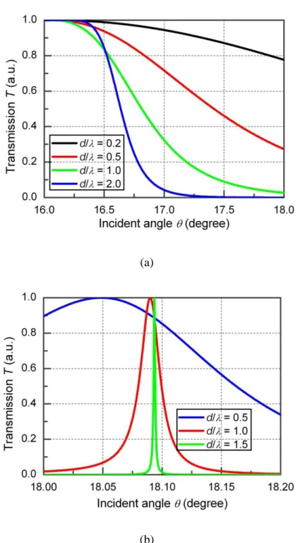
3.1.3 Transmission versus incident angle ...42
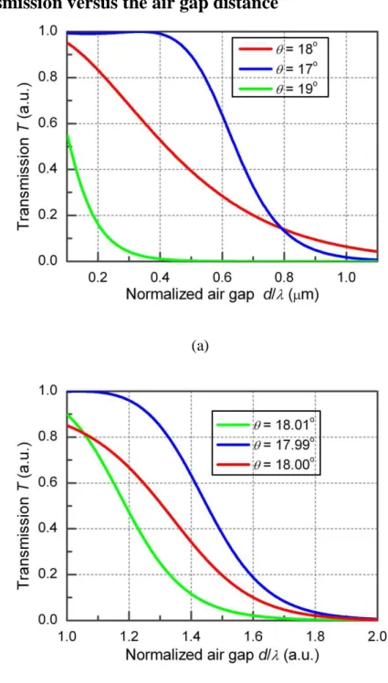
3.1.4 Transmission versus the air gap distance...45
3.1.5 Transmission versus the refractive index change ...49
3.1.6 Transmission versus the central rib width ...54
3.2
MEMS thermo-optical switch...563.2.1 Design of the thermo-optical switch. ...56
3.2.2 Fabrication of thermo-optical switch ...62
vii
3.3
MEMS switchable polarizer ...693.3.1 Design of the MEMS switchable polarizer ...70
3.3.2 Fabrication of the MEMS switchable polarizer ...73
3.3.3 Experimental results and discussions...74
3.4
Optical tunneling junction ...793.4.1 Design of the optical tunneling junctions ...80
3.4.2 Experimental results and discussions...85
3.5
Summary...864.
Slow light metamaterial waveguide
...864.1
Design of metamaterial slow light waveguide...874.2
Basic study on fishnet unit cell...944.2.1 Design of unit cell ...94
4.2.2 S-parameter analysis ...98
4.3
Design of coupled SRR unit cell structure. ...1044.3.1 Inner and outer ring design ...104
4.3.2 S-parameter analysis ...112
4.4
Tuning of the group velocity ...1164.5
Discussion on absorption...118viii
5.
Tunable metamaterial via MEMS technology
...1215.1
Design of the tunable metamaterial ...1235.2
Numerical results and discussions ...1275.2.1 Electrical response ...127
5.2.2 Magnetic response ...134
5.3
Fabrication of the tunable metamaterial. ...1375.4
Experimental results and discussions ...1455.4.1 Electrical response ...145
5.4.2 Magnetic response ...150
5.4.3 Light speed modulation...160
5.5
Summary...1656.
Conclusions and Recommendations
...1686.1
Conclusions...1686.2
Recommendations...170Author’s Publications
...173ix
LIST OF FIGURES
Fig. 2.1 Schematic of optical tunneling on 1D photonic structure.
Fig. 2.2 Schematic of Fabry-Pérot micro-cavity. (a) the plane mirror FP
micro-cavity, (b) the curved mirror FP micro-cavity and (c) the Bragg mirror FP micro-cavity.
Fig. 2.3 Schematic of 2D photonic crystal micro-cavity.
Fig. 2.4 Schematic of whispering gallery mode micro-cavity.
Fig. 2.5 The schematic of a mechanical optical switch. (a) signal light is
switched to output fiber 2 (b) signal light is switched to output fiber 1.
Fig. 2.6 (a) The schematic of all optical switch based on 2D photonic crystal cavities. (b) The change of the refractive index as the function of pumping light power and the length of the central resonator.
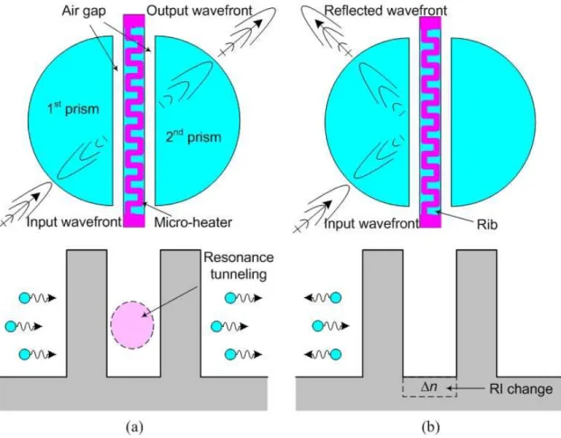
Fig. 3.1 Optical barrier structures and their tunneling effects. (a) Top view
of the single optical barrier structure that has a thin air gap sandwiched between two hemispherical prisms; (b) top view of the double optical barrier structures, which has an addition central rib in the middle and has two thin air gaps; (c) optical tunneling effect
13 15 17 20 22 37 11
x
through the single optical barrier, which can have only partial transmission; and (d) optical tunneling effect through the double optical barriers, which supports full transmission due to the resonance between the barriers.
Fig. 3.2 Analytical model of the double optical barrier structure.
Fig. 3.3 The transmission versus incident angle at different air gap distances for both (a) single optical barrier and (b) double optical barrier.
Fig. 3.4 The transmission versus air gap d at different incident angle for both
(a) single optical barrier and (b) double optical barrier.
Fig. 3.5 The contour map of single barrier transmission at different incident
angles and air gaps.
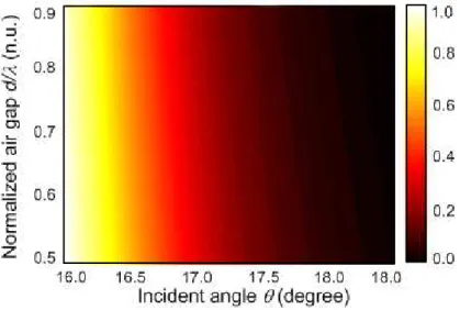
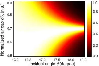
Fig. 3.6 The contour map of double optical barriers transmission at different
incident angles and air gaps.
Fig. 3.7 The transmission versus the refractive index change of single barrier structure.
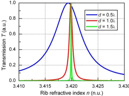
Fig. 3.8 The transmission versus the refractive index change of double barrier structure at different air gap width.
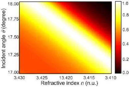
Fig. 3.9 The contour map of single barrier transmission versus the incident angle and refractive index.
39 42 45 46 47 49 50 51
xi
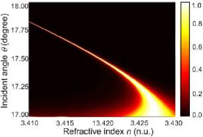
Fig. 3.10 The contour map of double barrier transmission versus the incident angle and refractive index.
Fig. 3.11 The transmission versus the central rib width g.
Fig. 3.12 Design and working principle of the optical double-well structure. (a) Top view and potential diagram in the ON state; (b) Top view and potential diagram in the OFF state.
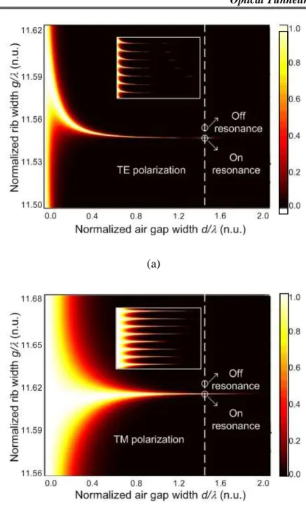
Fig. 3.13 Contour map of (a) TE and (b) TM light transmission as functions of d/λ and g/λ. Inset shows Transmission states of larger region. Fig. 3.14 The lens radius versus fiber distance at different incident
wavelength.
Fig. 3.15 Scanning electron micrograph of the fabricated thermo-optic switch.
Fig. 3.16 Experimental setup of the thermo-optical switch.
Fig. 3.17 Transmission spectrum of the optical switch. The blue solid line
refers to the off-state of the optical switch and the red dotted line refers to the on-state.
Fig. 3.18 The static tuning process of the thermo-optical switch. The transmission is measured at different pumping current. The red dotted line shows the experimental results and the blue line shows
the simulation results.
57 56 54 52 61 63 64 65 66
xii
Fig. 3.19 The dynamic tuning process of the thermo-optical switch. The transmission is measured as the function of time. The blue solid line shows the optical output power.
Fig. 3.20 The dynamic tuning process of the thermo-optical switch. The transmission is measured as the function of time. The blue solid line
shows the normalized optical output power. The red dashed line shows the pumping voltage generated by the SMU.
Fig. 3.21 The schematic of MEMS switchable polarizer.
Fig. 3.22 Contour map on the transmission versus different temperature and incident angle for both TE and TM polarized light. Inserts show the large scale of the contour maps.
Fig. 3.23 The transmission as the function of the refractive index change of the central rib for the input wavelength at 1550 nm.
Fig. 3.24 Scanning electron micrograph of the fabricated switchable polarizer.
Fig. 3.25 The experiment setup of the MEMS switchable polarizer.
Fig. 3.26 The normalized transmission versus the polarization rotation angle at different incident angles. The green triangle, red circular and blue square represent the normal incidence θ = 0°, refraction θ = 10° and tunneling θ = 18° respectively. 70 68 67 71 72 73 74 75
xiii
Fig. 3.27 The normalized transmission versus the heating current of the micro-heater. The blue triangle dashed line represents the TE polarized light and the red square dashed line represents the TM polarized light.
Fig. 3.28 Experiment results of MEMS switchable polarizer. (a) the static
switching process of the PER as the pump current increase. (b) the dynamic response of the polarization state of the output when pumped with periodically changed heating current. The dashed line shows the time variation of the pumping current.
Fig. 3.29 The schematic of optical tunneling junction.
Fig. 3.30 Electric field distribution of optical tunneling junction when the rib temperature is (a) 293 K and (b) 310 K respectively.
Fig. 3.31 The schematic of the reconfigurable WDM system integrated by optical tunneling junctions.
Fig. 3.32 The contour map of the transmission of the tunneling junction at
different incident wavelengths and rib widths.
Fig. 3.33 Scanning electron micrograph of the reconfigurable WDM system.
Fig. 3.34 Experiment results of the output wavelength at different rib width.
Fig. 4.1 Schematic of magnetoinductive slow light waveguide. (a) coupling within a single layer (b) coupling between two layers.
76 77 80 81 83 84 85 86 88
xiv
Fig. 4.2 The schematic of the tunable metamaterial. (a) before the substrate
refractive index change the resonance frequency is λ1. (b) after the
substrate refractive index change via the external pumping, the resonance frequency is λ2.
Fig. 4.3 The 3D contour map showing the (a) electric field and (b) magnetic field distribution of the fishnet unit cell. The side wall length of the
central square L = 3.5 µm. The metal strip width W = 1.5 µm. The period P = 9 µm. The metal thickness t = 0.3 µm and the substrate thickness D = 1.2 µm.
Fig. 4.4 The schematic of the tunable metamaterial. (a) before the substrate
refractive index change the resonance frequency is λ1. (b) after the
substrate refractive index change via the external pumping, the
resonance frequency is λ2.
Fig. 4.5 the 3D contour map showing the (a) electric field and (b) magnetic
field distribution of the fishnet unit cell. The side wall length of the
central square L = 3.5 µm. The metal strip width W = 1.5 µm. The period P = 9 µm. The metal thickness t = 0.3 µm and the substrate thickness D = 1.2 µm
Fig. 4.6 The calculated S-parameter of the fish net metamaterial. S11
represented by the blue line is the amplitude of the reflection 90
92
98 94
xv
coefficient and the red line shows the transmission coefficient amplitude S21.
Fig. 4.7 The calculated group index Ng versus the frequency at different substrate refractive index. The blue and red lines represent the group index when the substrate permittivity is 11.9 and 12.0
respectively.
Fig. 4.8 The schematic of coupled split ring unit cell
Fig. 4.9 The resonance frequency change versus the gap width. The blue, red
and green lines show the change of the gap width at different positions.
Fig. 4.10 The resonance frequency change versus the gap width. The blue and red line shows the gaps change of the lower split ring and upper split ring.
Fig. 4.11 The resonance frequency change versus the gap width. The blue and red line shows the gaps change of inner and outer gaps width
respectively and the green line shows the effects when all the gap widths are changed.
Fig. 4.12 The resonance frequency change versus the buried aluminum bar length. The blue and red line shows the bar length change of the split ring unit cell near and far from the incident EM wave
103 106 107 108 109 105
xvi
respectively and the green line shows all the bar length changed simultaneously.
Fig. 4.13 The resonance frequency change versus the film width.
Fig. 4.14 The resonance frequency change versus the substrate thickness.
Fig. 4.15 (a) S-parameters of the unit cells as the function of incident
frequency, (b) optical impedance of the unit cell of the metamaterial slow light waveguide ( sub = 12). The blue line shows the real part
of the impedance and red line shows the imaginary part of the
impedance.
Fig. 4.16 (a) The effective permittivity εeff and (b) the effective permeability
µeff versus the substrate permittivity εsub for both the coupled SRR
lattice and the single SRR lattice. The frequency of incident light is
38.65 THz which is the resonant frequency of the single SRR unit
cell. The change of the substrate permittivity εsub is 0.5. The εeff of
coupled SRR lattice and the single SRR lattice have the tuning
range of 18.42 and 0.25 respectively. The µeff of coupled SRR
lattice and the single SRR lattice have the tuning range of 0.8874 and 0.038 respectively.
Fig. 4.17 The group index as a function of the substrate permittivity. The incidence frequency is 43.73 THz. The propagated light is tuned
110
111
112
114
xvii
from a slowed backward wave to a tunneling wave in response to a change of substrate permittivity by 0.025.
Fig. 4.18 The absorption per unit cell (a) at different incident frequencies (b) at different substrate permittivity.
Fig. 5.1 Schematic of the tunable metamaterials using MEMS technology. (a) the top view of the tunable metamaterials. The frame part is connected with the comb drive which is used to tune the gap of
within the unit cells. (b) The unit cell consists of two semi-square split rings separated by a small gap G. One is movable while the other is fixed. In the initial state the unit cell is in the “[ ]” shape.
The unit cell can be changed to (c) the shape “ ” and (d) the shape
“I” by simply translating all the movable rings at the same time. W
is the width of the metal strip and R is the side length of the split ring.
Fig. 5.2 Equivalent circuit analysis of the tunable metamaterial unit cell. (a) shows the schematic of the unit cell. The “+” and “-” stand for the accumulation of the electrons induced by the external electric field.
(b) the equivalent circuit of the unit cell (a). (c) and (d) show the capacitance change during the gap increasing.
Fig. 5.3 Numerical analysis on the side wall length effect of the split ring metamaterial. (a) the transmission spectrum. (b), (c) and (d) shows
118
123
125
xviii
the electric field distribution when R = 35 µm, R = 30 m and R = 25 µm respectively.
Fig. 5.4 Numerical analysis on the different period of the split ring metamaterial. (a) the transmission spectrum. (b), (c) and (d) shows
the electric field distribution when P = 40 µm, P = 30 µm and P = 25 µm respectively.
Fig. 5.5 Numerical analysis on the different gap width G of the split ring metamaterial. (a) the transmission spectrum. (b), (c) and (d) shows
the electric field distribution when G = 2 µm, G = 5 µm and G = 10
µm respectively.
Fig. 5.6 The simulated reflection spectrum of the tunable metamaterial at different incident angles. (a) with (b) without perpendicular
magnetic field component to the surface of the unit cell.
Fig. 5.7 Schematic of the process flow for tunable metamaterials. The
fabrication process flow consists of eight steps which are shown from (a) to (h). The inserts show the legend of the colors which represent different materials.
Fig. 5.8 Scanning electron micrographs of the fabricated tunable magnetic metamaterial. (a) Overview of the structures and (b) close-up of the unit cells. 130 132 139 143 135
xix
Fig. 5.9 The schematic of the experiment setup.
Fig. 5.10 The measured transmission spectrum at different gap width (G =1
µm black dotted line with square, G = 2 µm red dotted line with circular, G = 3 µm blue dotted line with triangle). The inserts shows the simulated electrical field distribution at each gap position.
Fig. 5.11 The measured dip frequency versus the gap tuning (red square). The
dashed line shows the simulation results.
Fig. 5.12 The schematic of the experiment setup.
Fig. 5.13 The measured reflection spectrum of the tunable metamaterial when
the incident EM wave is (a) TE and (b) TM polarized. The spectrum is measured at different incident angles (black 15°, red 30° and green 45°).
Fig. 5.14 The reflection spectrum of the tunable metamaterial when the gap is
tuned from 0 µm to 8 µm with a step of 2 µm. The different colors stand for different gap width (black 0 µm, blue 2 µm, green 4 µm, red 6 µm and pink 8 µm).
Fig. 5.15 (a) The effective permeability m at different gap width G. The
effective permeability is derived from the reflection coefficient using the Fresnel fit method. (b), (c) and (d) show the surface
current when the gap width is 2 µm, 0 µm and 8 µm respectively.
147 149 151 152 159 154 146
xx Fig. 5.16 The experiment setup of THz-TDS.
Fig. 5.17 The Detector signal as the function of time for both closed ring G =
0 µm (closed ring) and G = 2 µm (split ring). (a) the Detector signal at a long time span. (b)
162
1
CHAPTER 1
INTRODUCTION
1.1
Motivation
More than 3000 years ago, ancient Chinese built beacon tower to deliver messages using the signal flame. Today, a single mode fiber with the core size around 9 micrometers can carry more than one trillion bits per second. To date, light is not only used as the medium of signals for telecommunications [1-10], but also used for laser
manufacturing, biological and chemical sensing, medical diagnostics and therapy, display technology, and optical computing etc. Therefore, controlling light with a faster, stable and low power consuming way becomes the goal pursued by researchers studying
photonic devices. Many switchable (or tunable) photonic devices such as tunable lasers [11-14], optical switches [15-20] and variable optical attenuators [21, 22] have been developed to meet the needs of vast applications. The bottleneck of further increasing the
performance of photonic devices always lies in the following two questions: How to reduce the device scale so that it can be integrated in to a photonic circuit? How to control the micro-scaled or even nano-scaled photonic devices?
Microelectromechanical Systems (MEMS) offers a technical platform to solve the above two problems [23-25]. MEMS is the technology using very small (micro-scaled)
2
devices. It is also called Nanoelectromechanical Systems (NEMS) when the devices become nano size. Different from the hypothetical vision of molecular nanotechnology or
molecular electronics, MEMS are made up of components between 1 to 100 micrometers in size (i.e. 0.001 to 0.1 mm) and MEMS devices generally range in size from 20 micrometers to a millimeter. Borrowing the ideas from large scaled devices, traditional
MEMS technology succeed in building micro-scaled devices based on micromachining processes. MEMS technology offers the integration of mechanical elements, sensors, actuators, and electronics on a common silicon substrate through microfabrication on silicon wafer or adds new structural layers to form the mechanical and electromechanical
devices. In this way, large size optical devices can be scaled down to micro-scale using the MEMS technology.
Generally speaking, there are two methods to control the propagation of the light within the tunable photonic devices. One method is to change the geometry of the
photonic devices to control the path way of the signal light. For example, a movable mirror is often used to change the direction of the reflected light in MEMS optical switches. The other method is to change the optical properties of the device compositing
materials such as the photonic switches. The first method is used in many MEMS optical devices. However, the switching time of the MEMS mechanical structures is typical at milliseconds. The second method attracts more and more research interests because of its
faster switching time.
The optical properties of the compositing materials of the photonic devices are often realized by stimulating the material using thermo, electrical or optical method.
3
However the changes of the optical properties are quite limited. Take silicon for example, the refractive index change of the silicon is typically less than 0.5%. Therefore, the
micro-optical resonators are often applied to enhance the effect of the compositing material change. In most cases, it is not feasible to simply scale down the optical cavities used in large scaled optical devices to build MEMS devices, because the size effects
might cause some problems in the performance of the micro-scaled devices. Therefore, the optical resonators have to be carefully designed to meet the needs of the micro-scaled photonic devices.
Metamaterials refers to the artificial materials the optical properties of which
relay on both the geometry of the unit cells and their compositing materials. The unit cells of metamaterials are sub-wavelength resonators of the incident light whose wavelength is typically ten times of the size of the unit cells. The size of the unit cells for THz metamaterials is around tens of micros which are the typical size for MEMS
devices. Therefore, the geometry of the THz metamaterial unit cells can be tuned by MEMS technology. It offers another method to make micro-scaled tunable photonic devices.
1.2
Objective
The ultimate objective of this PhD project is to design micro-scaled tunable photonic devices which have merits of low power consumption, fast tuning speed, large
tuning range and small device scales etc. To achieve this objective, two different approaches have been studied in this thesis: The first one is to apply MEMS technology
4
to double optical barrier structure the signal light of which is transmitted via resonance tunneling effect. The other approach is to use MEMS structure to tune the geometry of
the THz metamaterial unit cells. In this way the material properties of the THz metamaterial can be changed for potential applications on tunable photonic devices.
The double optical barriers structures are often used to study the super luminance effects. In this PhD project, the frustrated total internal reflection (FTIR) structures are
realized using MEMS technology to control the propagation of the signal light. A numerical analysis method is developed to study and optimize the parameters of the FTIR structure and five different tunable photonic devices are demonstrated.
In order to demonstrate the possibility of combine the MEMS technology with metamaterial structures, a numerical study on a tunable slow light waveguide is first
given and then followed by the demonstration of a tunable magnetic metamaterial.
1.3
Major contributions
The major contributions of this thesis are summarized as the following:
A thermo-optic switch is realized based on optical double optical barrier structure, which has a high-low-high-low-high refractive index construct formed by
micromachined silicon prisms and air gaps. Analysis shows such structure features full
transmission (i.e., ON state) and requires low refractive index change for switching function. The device is fabricated on silicon-on-isolator wafer using deep etching process.
5
A switchable polarizer is demonstrated using the double optical barrier structure.
In experiment it measures a PER of lager than 23 dB when the pumping current is above
60 mA. The switching time is shorter than 125 µs which is limited by the polarization analyzer used in the experiment.
A MEMS tunable add-drop multiplexer is realized by applied the optical tunneling structure to the ribbed waveguide. The tunable add-drop multiplexer is based
on Y-shape optical double barriers tunneling junction which are realized by MEMS
technology. In the experiment, a five-channel prototype of the tunable add-drop multiplexer is demonstrated. The measured output is ranged from 1549.24 nm to 1559.21 nm.
A tunable slow light metamaterial via tuning the substrate refractive index is numerically studied. The couple SRR unit cell is finally proposed and numerically
characterized. The simulation results show that the coupled SRR design improves the tunability of the effective permittivity and the effective permeability by 70 and 200 times,
respectively The required permittivity change is only 0.025, which can be achieved by either thermal-optic effect or photon induced free carrier effect of the semiconductor materials. It may find potential applications in data storage, photonic circuits, optical communications and bio-sensors.
A tunable metamaterial using the MEMS technology is numerically analyzed and experimentally demonstrated. The effective permeability of the tunable magnetic
6
frequency. It demonstrates a unique approach to control the optical properties of metamaterials via changing the geometric dimensions and shapes of the unit cells.
1.4
Organization of the thesis
This thesis is focused on the design and experiment of the tunable photonic
devices based on MEMS technology which is divided into six chapters:
Chapter one gives a brief introduction of the motivation, objective, major contribution and organization of the thesis.
Chapter two gives the literature survey on optical resonators, tunable photonic devices and tunable metamaterials.
Chapter three demonstrate MEMS devices based on optical tunneling effects.
Firstly, the frustrated total internal reflection (FTIR) optical barrier structure is presented and its transmission states are numerically studied via transfer matrix method (§3.1). The design of MEMS optical double barriers switch will be first elaborated, followed by the
theoretical and experimental analyses is shown in §3.2. Then, the application of the MEMS optical double barrier structure as the switchable polarization beam splitter is shown in §3.3. The optical tunneling effect is combined with the rib waveguide and form a reconfigurable optical tunneling junction is shown in §3.4 and followed by its
applications on the wavelength de-multiplex system. Finally the conclusion is shown in §3.5.
Chapter four is focused on the tuning of the slow light metamaterials via the
7
limited by the material properties of the substrate, the tuning range of which is normally not very large. The objective of this chapter is to find a new metamaterial structure which
can enhance tunability of the tunable metamaterials. Furthermore, the tuning of the group velocity index of such tunable metamaterials is also numerically studied. This chapter is organized as follow: The design of the slow light waveguide constructed by
metamaterials is shown in §4.1. The fishnet unit cell is analyzed in §4.2 as a possible candidate for the building blocks of slow light waveguide. A coupled SRR unit cell is given in §4.3 for better tunability. The tuning of the material properties and slow light group index on a fishnet metamaterial is shown in §4.4. The discussion on absorption is
given in §4.5.
Chapter five shows a new way to tune the optical properties of the metamaterials. This tuning method combines micromachined technology with the design of the
metamaterial unit cells. It can make the metamaterials tunable without exciting their compositing materials. Therefore, the tunablility of the metamaterial is no longer limited by the refractive index change of the nature materials. In this chapter, a split ring structure is selected to demonstrate the tuning method. The electrical and magnetic
response of the tunable metamaterial is demonstrated both numerically and experimentally. This chapter is organized as follows: The design of the tunable metamaterial is given in §5.1. The numerical analysis of the tunable metamaterial is
shown in §5.2 and followed by the fabrication (§5.3) and experimental demonstration in §5.4. Finally the summary is given in §5.5.
8
CHAPTER 2
LITERATURE SURVEY
In this chapter, the literature survey of optical tunneling, micro-cavities, optical switches, slow light waveguide and metamaterials are presented. The optical micro-cavities are the key components for the micro-scaled photonic devices tuned by changing the material properties of the compositing materials which is faster and more stable than
those devices tuned by the mechanical method. Here the optical micro-cavities are categorized by their geometry and summarized by their quality factors. The micro-scaled optical switches are presented to be compared with our approaches in Chapter 3. Finally,
the survey of metamaterials is presented.
2.1
Survey of optical tunneling
2.1.1 Definition of the optical tunneling effect
Optical tunneling effect refers to the phenomenon of photons penetrating through
the classically impenetrable barriers (e.g., the interface where the total internal reflection occurs, photonic bandgap, metal layer, etc.), similar to the electron tunneling through the quantum barriers. Such effect has attracted broad interest of physical studies for both
9
the classical theory of electromagnetic waves and quantum physics. In particular, the optical tunneling effect is indispensable to the experimental study of tunneling process.
Since the wavelength of light is around 1 µm, optical tunneling structures are on order of micrometers compared to the nanometer-scale electron tunneling structures. Additionally, the optical tunneling is not complicated by other side effects such as electron-electron couplings.
According to the quantum physics, all particles, including photons, can tunnel
trough barriers which classically impossible for them to go through. Photons can tunnel through the optical barriers such as the photonic band gap, mental, above-critical-angle air gap (FTIR effect) and show great similarity to the electron tunneling effect. For decades, the analogy between the photon tunneling and electron tunneling has been
widely studied because the longer wavelengths of the photons bear great advantage in experiments [26, 27].
According to resent research on the analogue of optical and electron tunneling effects, identical transmission probabilities can be obtained from the two dimensional
Maxwell equations for photons and the one dimensional Schrödinger equations for electrons by making the equivalence as below [28],
10
where m, V0 and E are the mass, barrier potential, and energy of the electron,
respectively; while ω, n and θ, n denote the frequency, medium refractive index and the incidence angle of the photon, respectively.
Consider the photon tunneling process within non-absorption single and double
optical barriers structures. When an optical wave incident on a single barrier structure, some of the photons tunnel through the barrier and others are reflected back. The amplitudes of the electric field reflected backward by different interfaces are geometric
proportional such that the elimination of the reflection will be impossible. However, the situation is a bit more complex when two optical barriers are taken into consideration. Similar to the electron tunneling cases which have been theoretically studied [29] and experimentally observed [30] quite a long time ago, the tunneling probability can be
greatly enhanced by the resonance of the photons between the two barriers. Furthermore, the total transmission condition can be achieved by adjusting the potential of the optical barriers and the distance between them. In another word, the optical barrier can be
bridged by placing another barrier beside it with proper distance and potential which is named as the resonance tunneling effect in both electron and photon multi-barriers.
2.1.2 Applications of the optical tunneling effect
In quantum physics, optical tunneling effects are often used for experimental demonstration of the superluminal effect. The superluminal effect, also named as the faster than light (FTL) effect, refers the propagation of information or matter with the
speed faster than the light. The superluminal effect has been proposed and studied for years shortly after the discovery of quantum mechanical tunneling. In 1930, the
11
discussion on the speed of the tunneling process is brought up. A approximate analysis on time dependent Schrodinger equations and the conclusion that the tunneling takes no
appreciable time was made. This conclusion had been discussed for 30 years until the quantum tunneling devices has been made based on thin film technology. Then the question is revised in an effort to understand the frequency limitations for tunneling
structures consisted of metal-insulator-metal thin film sandwiches and an analytical expression for the time delay in barrier tunneling which suggests a finite and short traversal tunneling time that saturates with distance was given. To date, although no direct experiment shows the tunneling speed of matter can be faster than the speed of
light, the experimental study on superluminal effect using optical tunneling structures remains an interesting research which has potential applications on communication and space travelling.
Fig. 2.1: Schematic of optical tunneling on 1D photonic structure
The experimental measurement of superluminal optical tunneling times in double
barrier photonic band gaps was demonstrated by [30]. The tunneling pulses is chosen to be 1500 nm in wavelength and the experiment is carried out on double barrier fiber Bragg gratings. The transit time is measured to be paradoxically short which implying the
12
superluminal propagation and the saturation effect on the barrier distance are also observed.
The other and maybe the most widely used application for optical tunneling effect
is the coupling of the photonic devices between sub-wavelength gaps. For example, optical tunneling effects has been used as the coupling between the waveguide and photonic micro-cavities, the coupling between the prism and metal surface for the
generation of the surface plasmon waves and the coupling between the laser head and cavities. In Chapter 3, the optical tunneling effect using frustrated total internal reflection will be used to design the thermo-optical switches.
2.2
Survey of optical micro-cavities
Dielectric optical micro-cavities are the key components for densely-integrated optical circuits. Most of the micro-cavities now used are large compared with the
resonance wavelengths which are the limits of the size of the micro-cavities. However, the structure size of the micro-cavities can be reduced to the order of the wavelength by using the compositing materials with large refractive index contrast. The optical
micro-cavities can be categorized into three different types by their geometry, such as the Fabry-Pérot (FP) cavity, photonic crystal micro-cavities and the whispering gallery micro-cavities etc.
13
2.2.1 Fabry-Pérot micro-cavities
The Fabry-Pérot (FP) micro-cavity is named after Charles Fabry and Alfred Perot who construct this optical micro-cavity as interferometer [26, 27]. The typical FP cavity is
constructed with a transparent plate with two reflecting surfaces, or two parallel highly reflecting mirrors (Fig. 2.1). Divided by their mirrors, the FP micro-cavities can be categorized by three different types: the plane mirror FP micro-cavities (Fig. 2.1(a)), the curved mirror FP micro-cavities (Fig. 2.1(b)) and the Bragg mirror FP micro-cavities (Fig.
2.1(c)). The plane mirror FP micro-cavities are the most basic type of the FP cavity and have been widely used in the applications such as laser cavities, etalon and filters [28, 29]. The curved mirror FP cavities can further focus the light due to the shape of its mirror
which reduces the scattering loss due to the mirrors. The Bragg mirror FP micro-cavities has larger Q factors than the cured mirror and plane mirror FP cavities because the Bragg mirror usually has a larger reflection coefficient.
14 (b)
(c)
Fig. 2.2: Different types of Fabry-Pérot micro-cavities. (a) the plane mirror FP cavity, (b) the curved mirror FP cavity and (c) the Bragg mirror FP cavity.
The transmission spectrum of FP micro-cavities as a function of wavelength exhibits peaks of large transmission corresponding to resonances of the micro-cavity. The transmission coefficient can be written as [30]
where T is the transmission coefficient, R is the reflection coefficient of the mirrors, d is the optical length between the two mirrors and λ is the wavelength.
The FP cavity is widely used in telecommunications and laser optics. The most important common applications are as filters, in which a series of thin film layers are
deposited on an optical surface by vapor deposition. Those multi thin film layers structures have similar geometries with 1D photonic crystal [30]. The FP cavity can also be used as the optical wavemeter, laser cavities and etalons etc. The FP optical cavities (2.2)
15
can be scaled down to micro size for densely-integrated photonic circuit. However the edge effects caused by the scattering of the light become obvious when the cavity size
become small enough to be compared with the wavelength.
2.2.2 Photonic crystal micro-cavities
Periodical structures with high refractive index contrast have recently become very interesting structures for light localization. The periodical structures, also called photonic crystals, can be designed to have the photonic bandgap which stop the light from propagating at all directions. Theoretically speaking, light can be trapped within a
very small region by constructing the confinement periodical structures at three dimensions (3D). However, 3D photonic crystals are not easy to be fabricated with the existing fabrication techniques [31, 32]. 1D photonic crystals derived directly from Bragg reflectors has already been widely used in commercial applications such as data
communications, laser cavities and sensors etc. 2D photonic crystals are fabricated using dielectric membrane with periodically patterned holes or arrays of small pillars which have been demonstrated in many works [33-37].
16
The photonic crystal micro-cavities can be designed to have not only very high quality factors (Q factor) but also very small mode volumes. The light can be localized
within a very small region according to the design. The typical lattices of the photonic crystals are one quarter of the resonance wavelength and the photonic crystal micro-cavities can be realized by simply remove or change the positions of the building blocks
(holes or pillars). Therefore, the size of the photonic micro-cavities can be scaled down the order of the wavelength. Furthermore, the lattice structures are very easy to be integrated with each other. However, the coupling of the light from outside to the photonic micro-cavities remains a problem. The large Q factor increased the light-matter
interactions which ensure the nonlinear tuning of the photonic crystal micro-cavities. However, the large Q factors also lower the threshold of the signal light induced nonlinear effect which limits the power of the signal thus decrease the signal noise ratio
(SNR).
2.2.3 Micro-cavities with whispering gallery mode
The whispering gallery modes are confined by continuous total internal reflection
of the cavity interface. One of the largest whispering gallery mode cavities is the temple of the heaven the size of which is around 5000 square meters. The resonant waves are the sound waves other than the optical waves. However, the whispering gallery mode cavities
can be scaled down to small enough to compare the resonant wavelength. In recent years, many different micro-cavities with whispering gallery mode have been studied, such as the micro-sphere cavities, the toroid micro-cavities and the micro-ring cavities [38-40].
17
The whispering gallery mode cavities have many applications such as micro-lasers, narrow filters, optical switching, ultrafine sensing, displacement measurements,
high resolution spectroscopy, Raman sources and studies of nonlinear optical effects.
Fig. 2.4: Schematic of whispering gallery mode (WGM) micro-cavity.
Similar to the photonic crystal micro-cavities, the whispering gallery mode
micro-cavities has merits such as, high Q factor, small mode volume and small size etc. The fabrication techniques remain challenging regarding the commercial applications. As the scattering loss dominate the total loss of most whispering gallery modes, the cavity surfaces have to the carefully polished.
Micro-cavities fabricated using dielectric materials, such as semiconductors, glass and polymers etc., are the key components for most of the tunable photonic devices which is modulated using the nonlinear effects. Dielectric micro-cavities can localize the light field within a very small volume thus have a high Q factor and enhanced
18
amplified and the resonant frequency of the micro-cavities can be shifted. This is the basic concept used in most micro-scaled tunable photonic devices which has been
intensively studied recently. However, the dielectric micro-cavities have the limitations as follows: Firstly, the power of the signal light is limited by the Q factor and compositing material of the micro-cavities. Signal light of large power may introduce the
nonlinear effect of the micro-cavities and cause the self-modulation. This problem can be solved by choosing the signal light wavelength at non-sensitive regions of the compositing materials. Another limitation of the micro-cavities is the narrow band width of the resonant spectrum. The working frequencies are typically chosen to be the
resonance frequency of the micro-cavities thus the spectrum can be very narrow band due to high Q of the micro-cavities. Finally, the dielectric micro-cavities control the light by modulate the electric field of the incident light waves. Dielectric micro-cavities cannot
directly affect the magnetic field without ferromagnetic components which limits their applications on magnetic resonance based devices such as superlens. In chapter three, a new approach is developed to design the tunable photonic devices based on MEMS technology.
2.3
Survey of optical switches
Optical switches often refers to the device that enables signals in optical fibers or
integrated optical circuits (IOCs) to be selectively switched from one circuit to another. In commercial term, optical switch often refers to the equipment that switches the signal light from one photonic circuit to another by electronically switching between fiber
19
transponders. Traditional MEMS borrow the ideal form the commercial optical switches and using movable mirrors or shutters to switch the light in micro-scaled photonic
circuits using electronically controlled actuators. In recent years, photonic switches which switch the pathway of the light using nonlinear effects attract more and more research interest due to their fast switching speed and low power consumption. In this section, the
optical switches are categorized by their switching mechanism.
2.3.1 Mechanical optical switch
The mechanical optical switches refer to those devices which change the path
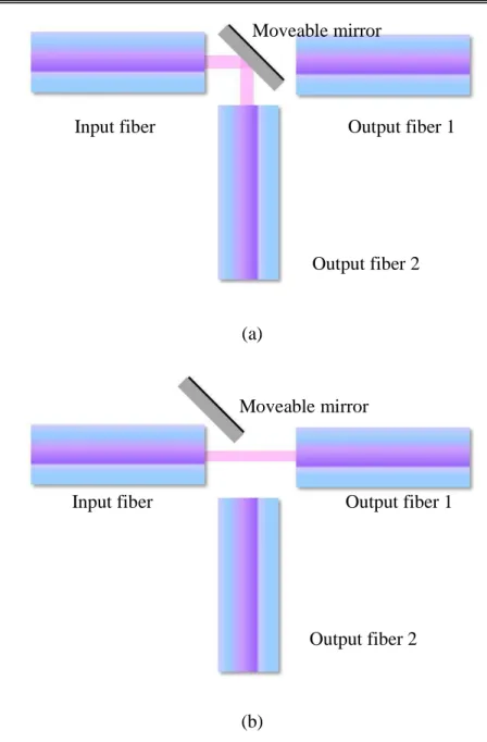
way of the light using the mechanically actuated moveable paths such as the movable optical fibers or mirrors [41-43]. Fig. 2.4 shows the schematic of a mechanical optical switch based on MEMS movable mirrors. The optical switch consists of four components: one input fiber, two output fibers and a movable mirrors. The input and
output fiber 1 is directly coupled to each other and the output fiber 2 is placed perpendicularly to the other two fibers. The signal light from the input fiber is reflected
90° to the output fiber 2 when a 45° tilted movable mirror is placed between the input fiber and output fiber one (Fig. 2.4 (a)). The signal light can be switched to output fiber 1 when the moveable mirror on longer block the signal light between the input fiber and
output fiber 1. In this way, the signal light from the input fiber can be switched between the output fiber 1 and 2 by mechanically change the position of the moveable mirrors [44, 45].
20 (a)
(b)
Fig. 2.5: The schematic of a mechanical optical switch. (a) signal light is switched to output fiber 2 (b) signal light is switched to output fiber 1.
This kind of the optical switches advanced in broadband switching and simple
geometry. However, the switching speed is limited by the mass of the movable parts. That is because the acceleration of the movable parts (fibers, mirrors) obeys the Newton’s
Input fiber Output fiber 1
Output fiber 2 Moveable mirror
Input fiber Output fiber 1
Output fiber 2 Moveable mirror
21
law while the force given by the actuator cannot be increased infinitely. The typical switching time of the mechanical optical switch in micro-scaled size is around several
milliseconds. Furthermore, the typical sized of the actuator is around several square millimeters which prevent the mechanical optical switches from being densely integrated.
2.3.2 Thermo-optical switch
The thermo-optical switch refers to those devices which switch the pathway of the signal light by the thermo-optical effect [46-47]. The thermo-optical switch can be divided into two groups. One is switching the light using thermo-expansion effect. For
example, the transmission the Bragg mirrors is highly depended on the lattice constant of each mirrors. When the lattice constant is change by the thermo effect, the transmission of the Bragg mirror of certain wavelength can be switched from 100% to 0%. In this way the Bragg mirror can be functioned as an optical switch. The switching speed of the
thermo-expansion is similar to that of the mechanical optical switch. As this kind of switching requires heating the whole mirror, the switching speed of the thermo-expansion optical switch might be even delayed by the heat diffusion process without cooling
system.
The other kind of thermo-optical switch is changing the refractive index of the optical micro-cavities via thermo-effect. For example, the thermo-induced refractive index of the silicon material can be expressed as follow [48]
22
The switching time of the thermo-optical switch is around microseconds since the localized heating is required only on the micro-scaled optical cavities. The expansion of
the crystal lattice for nature crystals is typically around microseconds. However, most thermo-optical switches have much longer switching time due to the lack of fast heating system and cooling systems which is not easy to be integrated to the micro-scaled
devices.
2.3.3 All optical switch
(a)
23
Fig. 2.6: (a) The schematic of all optical switch based on 2D photonic crystal cavities. (b) The change of the refractive index as the function of pumping light power and the length
of the central resonator.
The concept of all optical switches derives directly from the ideal of all optical networks (AON) or all photonic circuit which, analogy to the electronic circuit, uses light wave communication exclusively within the network. In this way the limitation of the
optical-electrical-optical (OEO) conversion can be circumvented. All optical switches are the building blocks for the optical transistors and optical logic gate. Practically speaking, the power of the signal light within the optical switch has to be comparable to the
triggering light so that it can be used in AON. Most of the reported all optical switches are, more precisely speaking, optical switches triggered by photon induced free carrier effect. For example, the all optical switch based on 2D photonic crystal cavities is shown in Fig. 2.5 (a) [49]. The refractive index of the central resonator is changed by the
vertically incident pumping light while the pathway of the signal light within the photonic crystal waveguide can be modulated. The free carrier effect on refractive index
change ∆n is plotted in Fig. 2.5 (b) using the following equations [48]
where ∆Ne and ∆Nh is the free carrier density induced by free electrons and holes
respectively.
24
The triggered light changes the refractive index of the optical switch compositing material thus changes the pathway of the signal light. Therefore, the power of the
triggered light are much stronger than that of the signal light which creates a bottleneck for the all optical switch applications. The typical switching time of the all optical switch is in the order of picoseconds which are limited by the carrier relaxation time.
Researchers in quantum optics are building all optical switches using photon-photon interactions which use one photon to control the transmission of the other. It might be a solution to the above mentioned problem. However, there are still many basic works unfinished.
Optical switches have been widely used in telecommunications, optical computations and biomedical chips. Of all the applications, the switching speed is always the most frequently concerned parameter of the optical switches which are limited by the following conditions: Firstly, the ultimate bottleneck of the switching time is the response
time of the compositing materials to each switching mechanisms. For example, the switching speed of the mechanical optical switches is limited by the moving speed and displacement required by the moving components such as the movable mirrors and
shutters. However the thermo-optical switch is limited by the material response of the thermo expansion and relaxation time of the crystal lattice. Therefore, changing the compositing material may be one solution to further increase the switching time. For
example, the optical properties of many nonlinear crystals, such as the liquid crystal, can be dramatically changed by the thermo or electrical excitations. Such nonlinear crystals can be used as the compositing material for the optical switches. For example, liquid
25
crystals are used in optical micro-cavities or Mach–Zehnder interferometer [50] for optical switching. However, the nonlinear crystals increase the fabrication difficulties and
are not suitable for densely-integrations.
2.4
Survey of slow light waveguides
Generally speaking, there are two procedures that can be used to control the group velocity of light. One of these is to exploit material resonances, such as the sharp absorption resonances of an atomic vapor. Control can be achieved, for example, by applying a strong optical field and using nonlinear effects to modify the optical response
experienced in a signal pulse, as in the work of Hau et al. Examples of this approach are electromagnetically induced transparency (EIT). In addition to EIT, there are several other sorts of material resonances that can be used to produce slow-light effects. There
has been particular success with the use of stimulated Brillouin scattering and the use of stimulated Raman scattering. In each of these processes, the strong gain feature induced by the presence of a strong pump field will also produce, as a consequence of the
Kramers–Kronig relations, a rapid spectral variation in the refractive index, which in turn leads to strong slow-light effects. The other procedure is to use material engineering to fabricate microstructured materials, such as arrays of microrings and photonic crystals that have artificially created resonances and optical responses. For instance, the group
velocity of light in a photonic crystal can be slowed down dramatically near the band edge of the photonic Brillouin zone. One particular example of this approach is the work
26
of Vlasov et al. at IBM, in which by appropriate patterning of a silicon waveguide a group index of 300 was produced, corresponding to a 300-fold reduction in the group
velocity.
In recent years, slow light has been intensively studied by two different groups of researchers divided by the frequency region they are interested in. One group of people
works on the optical region. They use dialectic only waveguide with large dispersion to slow the light down by resonance. For example, the coupled resonance optical waveguide (CROW) is used for slow light purposed since the photon life time in the high Q optical cavities are very long. Generally speaking the electric response of the wave-guiding
structure is tailored by introducing the artificial structures. The other groups of researchers work on slow backward waves established in engineering practice giving rise to both microwave tubes [51] and to antennas [52]. Waves propagating on coupled LC
circuits were investigated by Atabekov [53] and Silin and Sazonov [54] as simple examples of periodic filters and slow wave structures which is similar as the CROW in the optical frequency region. An antenna array shown in [55] excited by a single element was shown to be able to support a leaky wave which is partially guided and partially
radiating. Slow waves can also be achieved by propagating the light along a set of spherical nano-particles [56-58], electrically coupled metallic rods [59], or a set of magnetically coupled loops as shown in [60, 61]. Those slow light waves generated by
tailoring the magnetic response of the wave-guiding structures are called magneto-inductive (or MI) waves. Metamaterials offers a platform to tailor both the electric and the magnetic response of the artificially engineered wave-guiding structures. Therefore,
27
both the electro-inductive and magneto-inductive slow light waves can be found in metamaterials.
2.5
Survey of metamaterials
This Metamaterials are artificially engineered materials, formed by integrating
various sub-wavelength unit cells, which can exhibit unconventional optical responses not observed in their individual compositing materials or in natural media. For example, negative, low, or near-zero permittivity or permeability can be observed in metamaterials with carefully designed unit cells. The negative refractive index can be observed in
certain frequencies when both the permittivity and the permeability are negative. Metamaterials, especially the negative refractive index metamaterials, have attracted a great deal of research interest in recent years [62-77]. The first experimental verification
of a metamaterial with negative refraction is demonstrated at microwave frequencies [78] using split-ring resonators predicted by Sir Pendry [79]. Experimental and theoretical studies of metamaterials which started in the microwave frequency region are steadily
moving into the higher frequency region. Recent experimental breakthroughs show the optical response of metamaterials in the THz, infrared, and visible frequencies [80-83] with the aid of the nano-fabrication techniques.
It is important to point out that the concept of metamaterials is not limited to the negative-index material. Other artificially engineered materials with unusual parameter
values, such as epsilon-near-zero (ENZ) materials [84, 85], epsilon-very-large (EVL) materials [86, 87], highly dispersive materials, and single-negative (SNG) media, may
28
offer exciting potential applications as well. For instance, using ENZ materials, it has been shown theoretically that the possibility of squeezing light through very narrow
channels and tight bends [88]. The ENZ materials which are used in transparency and cloaking are also shown in [89, 90]. Generally speaking, metamaterials provide a platform for dispersion engineering and management which means the dispersion of the
materials can be designed by changing the geometry of their unit cells. It is a direct method to modulate and tailor electromagnetic waves. For example, it is well known that by stacking pairs of thin layers of plasmonic material (e.g., Ag) and conventional dielectric, one can form an anisotropic metamaterial whose permittivity tensor elements
can achieve near zero or very high values [91] which cannot be achieved by bulk materials with single composition.
2.5.1 Magnetic metamaterials
Magnetic metamaterials consisting of artificially designed unit cells with a strong magnetic response have been developed into an important branch of the metamaterials
research. For example, the split ring resonator unit cell is designed for strong magnetic response which was investigated in [92-99]. Many works have been down in different forms of split ring structures. One of the split ring structures with broadside coupling is
proposed in [100], another structure, namely the twin split ring, was proposed in [101], and a three-dimensional set of rings, isotropic split ring, was introduced in [102]. The singly split ring was known before as a broken loop [103, 104]. The split pipe [105, 106] is a novel bulk variant of the single ring resonator without need of a substrate; it was also
29
described by Schelkunoff and Friis [108] and later used by Wiltshire et al. and by Mossalaei et al. [109]. Other metamaterial unit cells with strong magnetic resonance are
also proposed, such as double circular elements [110], chiral, double-helix particles, the Swiss Roll [111] and the Spiral Resonator [112] etc. Other metamaterials using particles are also demonstrated such as “castle” rings [113], “labyrinth” rings [114], or
“metasolenoids” [115]. The development of the field of magnetic metamaterials has taken a new turn when miniaturization of split rings using microfabrication was employed to increase the magnetic resonance frequency of meta-materials to 1 THz (300 µm wavelength) [116]. Nanofabrication led to further increase of the magnetic resonance
frequency first to 100 THz (3 µm wavelength) [117] and most recently to the visible range [118-120]. Novel nanoparticles such as a pair of closely spaced nanostripes or
nanorods [121, 122], the nanostructured U-particle [123, 124] and the nanostructured “
crescent” [125] were introduced. The magnetic metamaterials open a gateway to tailor the magnetic response of the artificial structures without introducing the ferromagnetic materials.
2.5.2 Tunable metamaterials
Metamaterials are the artificial materials with many properties which may result
in the applications which cannot be realized by nature materials, such as invisibility cloaks, negative refraction and perfect lenses [126-130]. However, metamaterials has drawback as follows: Firstly, the significant frequency dispersion caused by the
resonance nature of the metamaterials leads to the narrow bandwidth and large metal absorption. Although narrow bandwidth is required for some applications, the