HAL Id: tel-01153249
https://tel.archives-ouvertes.fr/tel-01153249v2
Submitted on 12 May 2015HAL is a multi-disciplinary open access archive for the deposit and dissemination of sci-entific research documents, whether they are pub-lished or not. The documents may come from teaching and research institutions in France or abroad, or from public or private research centers.
L’archive ouverte pluridisciplinaire HAL, est destinée au dépôt et à la diffusion de documents scientifiques de niveau recherche, publiés ou non, émanant des établissements d’enseignement et de recherche français ou étrangers, des laboratoires publics ou privés.
superconducting NbN
Clementine Aberkane
To cite this version:
Clementine Aberkane. Nano-scale electronic inhomogeneities in ultra-thin superconducting NbN. Solid mechanics [physics.class-ph]. Université Pierre et Marie Curie - Paris VI, 2014. English. �NNT : 2014PA066644�. �tel-01153249v2�
École Doctorale de Physique et Chimie des Matériaux - ED 397
Thèse
Soutenue le 24 octobre 2014
Pour l’obtention du grade de
docteur de l’université Pierre et Marie Curie
Discipline : Physique des solidespar
Clémentine
Nano-scale electronic inhomogeneities in
ultra-thin superconducting NbN
Co-dirigée par M. Dimitri Roditchev et M. Christophe Brun
Composition du jury :
Mme Hélène Bouchiat examinatrice M. Christophe Brun co-directeur M. Claude Chapelier rapporteur Mme Claire Marrache-Kikuchi rapportrice M. Dimitri Roditchev directeur M. Abhay Shukla examinateur
Institut des Nanosciences de Paris Case 840
4, Place Jussieu 75 252 Paris Cedex 05
École doctorale Physique et Chimie de Matériaux Case 115
4 place Jussieu 75 252 Paris cedex 05
Abstract
Superconductor-insulator transition in NbN ultra-thin films
In order to better understand the various processes taking place at the superconductor-insulator transition (SIT), we have probed simultaneously the global and local electronic properties of NbN ultrathin films, elaborated ex-situ on sapphire substrate. The transi-tion was approached by reducing the films thickness, increasing the normal state square resistance to several kiloOhms. The corresponding Tc’s of the studied films ranged from about Tc ∼ 15K, which is close to TC−bulk, to Tc ∼ 3.8K (Tc/TC−bulk∼0.23). In the range
0.4TC−bulk<Tc< TC−bulkresistivity measurements are consistent with Finkelstein’s
reduc-tion of Tc induced by disorder and electron-electron repulsion. Local scanning tunneling spectroscopy (STS) measurements show the emergence of granularity in the supercon-ducting properties upon Tc reduction, as well as the progressive development of a strong Altshuler-Aronov background in the dI/dV(V) tunneling spectra, in agreement with Fin-kelstein scenario. For the most disordered film (Tc ∼ 3.8K), simultaneous in-situ resistivity and STS measurements allowed us to follow at the same sample area the evolution of these emergent granular superconducting properties as a function of temperature and magnetic field, which demonstrate a percolative behavior of the transition to the bad-metal normal state. This local picture finds an interesting signature in the change of the dimensiona-lity of the Aslamasov-Larkin fluctuations above Tc from 2D to 0D. Besides, such a study is particularly interesting to better understand the various phenomena occurring in and limiting the behavior of single-photon detectors patterned out of NbN films.
Keywords
Superconductor-insulator transition, disordered superconductors, scanning tunnelling microscopy and spectroscopy (STM/STS), superconductivity, ultra-thin films, NbN, single photon detectors
Transition supraconducteur-isolant dans des films minces de NbN
Afin de mieux comprendre les différents processus qui apparaissent à la transition supraconducteur-isolant (SIT), nous avons sondé simultanément les propriétés électro-niques globales et locales de films ultra-minces de NbN, élaborés ex-situ sur un substrat de saphir. La transition isolante a été approchée en réduisant l’épaisseur des échantillons, augmentant la résistance par carré de l’état normal jusqu’à plusieurs kiloOhms. Les Tc cor-respondant aux films étudiés varient de Tc ∼ 15K qui est proche de TC−bulk à Tc ∼ 3.8K
désordre et les intéractions électron-électron. Les mesures de spectroscopie tunnel locale (STS) montrent l’émergence d’une granularité dans les propriétés supraconductrices en réduisant la Tc, ainsi que le développement progressif d’un fort fon Altshuler-Aronov dans les spectres tunnel dI/dV(V), ce qui est en accord avec le scenario de Finkelstein. Pour l’échantillon le plus désordonné (Tc ∼ 3.8K), des mesures de résistance in-situ et de STS en simultané nous ont permis de suivre sur la même zone de l’échantillon, l’évolution des propriétés supraconductrices de cette granularité émergente en fonction de la température et du champ magnétique, qui ont démontré un comportement percolatif de la transition dans l’état normal de mauvais métal. Cette étude locale a trouvé une confirmation dans le changement de dimensionnalité des fluctuations Aslamasov-Larkin au-dessus de Tc de 2D à 0D. En outre, une telle étude est particulièrement intéressante pour comprendre les différents phénomènes qui se produisent, limitant le fonctionnement des détecteurs de photon unique basé sur les films de NbN.
Mots-clefs
Transition supraconducteur-isolant, supraconducteurs désordonnés, microscopie et spec-troscopie à effet tunnel (STM/STS), supraconductivité, films ultra-minces, NbN, detecteur de photon unique
Contents
Introduction 13
1 Experimental context: introduction to the superconductor-insulator
tran-sition and state-of-the-art 17
1.1 Granular versus homogeneous systems in the superconductor-insulator
tran-sition . . . 18
1.1.1 Granular thin films . . . 18
1.1.2 Homogeneous thin films . . . 21
1.2 Theory for the superconductor-insulator transition . . . 22
1.2.1 Bosonic scenario . . . 22
1.2.2 Fermionic scenario . . . 25
1.2.3 Fractal pseudo-spin model and numerical methods . . . 26
1.3 Recent results . . . 29
1.3.1 Scanning tunneling spectroscopy measurements . . . 29
1.3.2 Transport measurements . . . 31
1.3.3 Other measurements . . . 35
1.4 Main results obtained during this thesis . . . 37
2 Sample fabrication process and characterization 43 2.1 Sample elaboration . . . 44
2.1.1 Substrate . . . 44
2.1.2 Vacuum deposition . . . 44
2.1.3 Evaporating conditions . . . 45
2.1.4 Thin films thickness determination . . . 45
2.2 Sample characterization . . . 46
2.2.1 Transmission Electron Microscopy measurements . . . 46
2.2.2 TEM Results . . . 47
2.3 Ex-situ transport measurements . . . 49
2.3.1 Preliminary measurements after deposition . . . 49
2.3.2 Detailed magneto-transport experiments . . . 50
2.3.3 Resistance evolution as a function of film thickness . . . 50
2.3.4 Resistance evolution as a function of time . . . 51
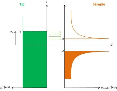
3 Experimental setups 53 3.1 Electron tunneling theory . . . 54
3.2 Tunneling spectroscopy of a superconductor . . . 56
3.3 Experimental aspects of STM . . . 57
3.3.1 Topographic mode . . . 57
3.3.3 Piezoelectric effect . . . 59
3.3.4 Vibration isolations . . . 60
3.4 Experimental setup M2 . . . 60
3.4.1 Specifications . . . 60
3.4.2 M2 makeover . . . 61
3.4.3 Operating tests and system limitations . . . 62
3.5 Experimental setup M3 . . . 63
3.5.1 Specifications . . . 64
3.5.2 in-situ transport measurements . . . 68
3.6 PPMS transport measurements . . . 69
4 Effect of magnetic field on the superconducting properties 71 4.1 Quantum phase transition . . . 72
4.1.1 General theory of scaling . . . 72
4.1.2 Predictions for the critical exponents . . . 73
4.2 Scaling law analysis in NbN . . . 74
4.3 Superconducting fluctuations . . . 78
4.3.1 Aslamasov-Larkin conductivity . . . 78
4.3.2 Experimental results . . . 79
4.3.3 Interpretation/Discussion . . . 81
4.4 High magnetic field study . . . 83
4.4.1 Introduction . . . 83
4.4.2 Magnetoresistance on NbN . . . 83
4.4.3 Interpretation of the negative magnetoresistance . . . 84
5 Effect of the film thickness on the superconducting properties 87 5.1 Introduction . . . 88
5.2 Electrical properties of the films . . . 88
5.3 Tunneling spectroscopy results . . . 89
5.3.1 Evolution of the tunneling spectra with the thickness . . . 89
5.3.2 Unconventional superconductivity close to the SIT . . . 92
5.4 Analysis of the results . . . 93
5.4.1 Effect of the magnetic field . . . 94
5.4.2 Effect of Coulomb interactions . . . 95
5.4.3 Does the passivation layer induce a proximity effect? . . . 96
5.4.4 Tunneling data : comparison with previous works . . . 98
6 Spectroscopic study of a thin film close to the superconductor-insulator transition 101 6.1 Experimental conditions . . . 102
6.2 Phase diagram . . . 103
6.3 Nanoscale spectroscopic properties at low temperature . . . 104
6.4 Temperature effect on the spectroscopic properties . . . 106
6.4.1 Evolution of the conductance map with the temperature . . . 106
6.4.2 Conductance map above Tc . . . 108
6.5 Magnetic field effect on the spectroscopic properties . . . 109
6.5.1 At 300mK . . . 109
6.5.2 At 2K . . . 111
6.5.3 At 4.2K . . . 113
Contents
6.6.1 Electron-electron interactions and disorder . . . 115
6.6.2 Modelling the zero-bias anomaly . . . 115
6.6.3 Experimental results . . . 116
6.7 Interpretation and discussion of the results . . . 119
7 Application: Toward a local study of superconducting nano-stripes used for single-photon detection 123 7.1 General informations about the single-photon detectors . . . 124
7.1.1 Introduction . . . 124
7.1.2 Parameters characterizing the performance of the detectors . . . 124
7.1.3 Detection principle . . . 124
7.1.4 Motivations . . . 125
7.2 Nanofabrication of the NbN detectors . . . 125
7.2.1 Sample preparation . . . 126
7.2.2 The resist . . . 127
7.2.3 Ionic etching . . . 127
7.2.4 The electronic lithography . . . 127
7.2.5 Final appearance of the sample . . . 127
7.3 STM/AFM measurements of a NbN meander . . . 128
7.4 Conclusion . . . 129
Conclusion 131
Introduction
The superconductor-insulator transition has been discovered several decades ago when decreasing the thickness of samples in order to search for superconductors with high criti-cal temperatures. Currently, the topic experiences a renewed success, in particular thanks to the new experimental contribution from local probe techniques. Moreover, it has been demonstrated that some superconducting features in disordered thin films show some sim-ilarities to what was observed in high Tc copper-oxide based superconductors. It boosted an additional interest of the physics community for this kind of thin films.
We have chosen smooth NbN thin films to study the superconductor-insulator transition. These samples are polycrystallines, and the superconductor-insulator transition can be tuned either by varying the magnetic field, the thickness of the NbN layer or also the films stoichiometry. The study of such samples is particularly interesting to better understand the microscopic processes responsible of the superconducting-insulating transition. The films used for this thesis work were elaborated by our collaborator Konstantin Ilin at the Karlsruhe Institute of Technology who also fabricates single-photon detectors patterned out from NbN films. This makes the study of these films even more interesting. Indeed, it has recently been demonstrated that the maximum detection efficiency occurs for films thicknesses close to the superconductor-insulator transition.
On one hand, this thesis work aims addressing several questions concerning the mech-anisms involved in the superconductor-insulator transition and, on the other hand, we would like to contribute to better understand the operating mode of single-photon detec-tors.
This thesis is organized in 7 chapters as described below:
Chapter 1: Experimental context: introduction to the superconductor-insulator transition and state-of-the-art
The study of the superconductor-insulator transition began several decades ago. There is a significant number of papers relating the results obtained both theoretically and exper-imentally, on a large variety of materials.
In this chapter, we compare the systems that exhibits a superconductor-insulator transi-tion discovered when decreasing the film thickness. Then, we describe the three scenario developed to explain the superconductor-insulator transition. These two parts are based on the thesis of Olivier Crauste [Cra10] that constitutes a very good review of these con-cepts.
Finally, we describe the international context in which the work done during this thesis has been performed. We try to give an overview of the previous recent works on the superconductor-insulator transition, by discussing the main results obtained with various
experimental techniques.
Chapter 2: Samples fabrication process and characterization
The homogeneous NbN thin films studied during this thesis were elaborated in Karlsruhe Institute of Technology by our collaborators. The structural properties of films play a key role in determining the electronic properties at low temperature. We used Transmission Electron Microscopy and transport measurements to characterize the samples both struc-turally and electrically. It enabled us to suggest that the SIT corresponds to so-called homogeneous transition and that in addition the resistance and the superconducting tran-sition temperature of the films evolve with time and thermal cycling. In this chapter, we describe the fabrication process of the NbN thin films and how we characterized it before further study.
Chapter 3: Experimental setup
Many techniques can be used to study the superconductor-insulator transition. However, Scanning Tunnelling Microscopy and Spectroscopy is a very promising tool since it gives a direct access to the local density of states. Combined with transport measurements, it becomes even more interesting because it enables one to compare the local conduc-tance measurements of the sample with the global conducconduc-tance. First, we have performed STM/STS measurements and transport measurements in separated experimental setups. Those results will be presented in chapter 5. Then we have used another more advanced setup and modified it to be able to measure in-situ the resistance of the thin films in the STM head. The results obtained are detailed in chapter 6.
After an introduction to electron tunnelling theory using the Bardeen work and Tersoff and Hamman work, we describe the experimental aspects of STM. Then, we depict the main characteristics of the experimental setups used during this thesis: STM M2, STM M3 and the Physical Properties Measurement System for the transport measurements. The next three chapters concern the experimental results we obtained when studying the superconductor-insulator transition on the NbN thin films.
Chapter 4: Effect of magnetic field on the superconducting properties
A great effort has been made during this thesis to characterize the samples by transport measurements. It finally lead to interesting results. First, we studied the superconductor-metal transition induced by varying the magnetic field. It enables us to suggest the exis-tence of a quantum critical point. Then, thanks to very high magnetic field measurements, we were able to drive the films to the normal state and to study the Aslamasov-Larkin fluctuations above the critical temperature.
After a review of the quantum phase transition theory and the different scenario that can be used to interpret the results, we present a scaling law analysis of our transport results obtained on NbN thin films.
Chapter 5: Effect of the film thickness reduction on the local superconducting properties
Before the beginning of this thesis, some results were already obtained in our group by scanning tunneling microscopy and spectroscopy on these NbN thin films. The superconductor-insulator transition has been approached by varying the thickness, reducing the critical temperature. The local superconducting properties probed by STS as a function of mag-netic field and the film thickness are presented in this chapter.
Contents
First, we show the transport characteristics of the studied samples. Then, we demonstrate the BCS-like behavior of thick samples and how it becomes more and more unconventional when approaching the insulating transition. In the last section of this chapter, we present an interpretation and discussion of the results with respect to the current literature. Chapter 6: Spectroscopic study of a thin film closer to the superconductor-insulator transition
In order to be able to measure in-situ, in the STM chamber, the resistance of the samples, we made some modifications of the experimental setup M3. It enables us to perform a fur-ther study of a sample which has a Tc of 3.8K, the closest to the superconductor-insulator transition among the studied samples. We succeeded to stay at the same place of the sample during all STS experiments and could realize a complete study of the B-T phase diagram (0T → 7T and 300mK → 7K) of the local tunneling characteristics. We also ex-amined in details the V-shape background on which the superconducting gap develops, and found that it is linked to strong electron-electron interactions effects in the presence of disorder.
First, the effect of the temperature on the local superconducting properties is shown and then the effect of magnetic field is presented. In the second part, the Altshuler-Aronov background is studied, an interpretation and a discussion of the results are presented at the end.
Chapter 7: Application: Toward a local study of superconducting nano-stripes used for single-photon detection
The NbN thin films studied during this thesis are also used to fabricate single-photon detectors. The operating principle of these detectors is described in the first section of this chapter. In order to study such a device, we used nanofabrication techniques with electronic lithography to elaborate a meander, starting from one of our NbN thin film. The fabrication process is thus explained in the second part of this chapter. Finally, we have measured the meander structure by using an AFM/STM. Unfortunately, due to tech-nical dysfunctions, we were not able to performed yet a spectroscopic STM study at low temperature. The AFM image of the structure obtained during this experimental run is shown in the last part of this chapter.
The conclusion summarizes the results obtained during this thesis and gives the out-look for the reminder of the study of the superconductor-insulator transition in thin films of NbN.
Chapter 1
Experimental context:
introduction to the
superconductor-insulator
transition and state-of-the-art
Contents
1.1 Granular versus homogeneous systems in the
superconductor-insulator transition . . . . 18
1.1.1 Granular thin films . . . 18
1.1.2 Homogeneous thin films . . . 21
1.2 Theory for the superconductor-insulator transition . . . . 22
1.2.1 Bosonic scenario . . . 22
1.2.2 Fermionic scenario . . . 25
1.2.3 Fractal pseudo-spin model and numerical methods . . . 26
1.3 Recent results . . . . 29
1.3.1 Scanning tunneling spectroscopy measurements . . . 29
1.3.2 Transport measurements . . . 31
1.3.3 Other measurements . . . 35
The study of the superconductor-insulator transition began several decades ago. There is a significant number of papers relating the results obtained both theoretically and experimentally, on a large variety of materials. The first two parts of this chapter are based on the thesis of Olivier Crauste [Cra10] that constitutes a very good review of these concepts.
1.1
Granular versus homogeneous systems in the
superconductor-insulator transition
It has been observed that when decreasing the thickness of some film, the Tc decreases. The first observation of this effect [STKC70], and the majority of the films showing the de-struction of the superconductivity when reducing the thickness were quenched-condensed [BA71, DGR78, DBC+80, OJG85]. It means that the substrate is maintained at low
temperature during the evaporation of the film. No particular precautions were made regarding the wetting layer on the substrate. These films are granular.
Then, it has been discovered that when adding a wetting layer onto the substrate before depositing the thin film, it is possible to synthesize more smooth and homogeneous thin films. A sublayer of Ge was often used [GB84]. Later on, smooth Pb and Bi thin films [HLG89] with no wetting layer have been realized and studied.
Thus, it is clear that the structural properties of the samples play a key role in determin-ing the electronic properties at low temperature. Thereby, the metallic films presentdetermin-ing a superconductor-insulator transition when decreasing the film thickness are commonly classified into two groups:
– Granular systems – Homogeneous systems
In perfectly crystalline thin films, synthesized in UHV conditions, superconductivity has been observed and studied down to a single atomic layer; it was the case of Pb or In which were analyzed by means of scanning tunneling microscopy and spectroscopy [ZCL+10]. A
superconductor-insulator transition has not been observed in such system upon thickness reduction.
The superconductor-insulator transition can be induced by varying the thickness but not only. Increasing the magnetic field, changing the doping or the disorder can also induce the transition.
1.1.1 Granular thin films
Granular systems can be described as an array of Josephson junctions. Indeed, the grains composing the film are embedded in an insulating matrix and coupled together thanks to the tunneling effect. To illustrate the behavior of the samples composing this group, the study of Jaeger et al. [JHOG89] will be taken as an example.
Granular thin films are characterized by a disappearance of superconductivity when reduc-ing their thickness in a way similar to what can be seen on figure 1.1. The superconductreduc-ing critical temperature remains almost constant when decreasing the thickness of the films but become wider : the zero-resistivity critical temperature decreases but the onset critical temperature Tc,onset at which the resistivity starts droping does not change much; even
for films close to superconductor-insulator transition.
Otherwise, a re-entrance phenomenon of the superconductivity is often observed in granular systems. The resistance starts to decrease when decreasing the temperature, sat-urate and finally increases back when further decreasing the temperature. It is a typical
1.1. Granular versus homogeneous systems in the superconductor-insulator transition
behavior of these systems. One important feature is also that the superconductor-insulator transition is observed when reducing the nominal thickness in a very narrow window of the order of few Angströms. For instance, in Ga samples (see figure1.1) [JHOG89], the thickness has been reduced only by approximately 2 Angströms between the lower and the upper R(T) curves.
For the insulating state, the evolution of the resistance as a function of temperature shows a characteristic activated exponential behavior associated to strong localization effects. Thus, the transition in granular thin films has been interpreted [Efe80, STKC70] as a competition between the Josephson coupling energy between grains and the Coulomb charging energy. Granular systems can be seen as an array of metallic particles embedded into an insulating matrix or separated by insulating grain boundaries. In the supercon-ducting state, the granules are coupled together by Josephson junctions. It means that Cooper pairs can tunnel from one granule to another. The Coulomb charging energy corresponds to the change in energy of a grain when adding or removing an electron. It plays a crucial role in the transport properties in the insulating regime when electrons are localized in the grains, such that the charge of each grain is quantized [BLVE07].
At last, the granular structure induces fluctuations of the phase of the superconducting or-der parameter, and these fluctuations become more and more important when approaching the insulating transition.
Figure 1.1: Evolution of R(T) curves for so-called granular superconductors a) Al, b) In,
c) Ga and d) Pb as a function of film thickness. In both cases, a superconductor-insulator transition is observed. (Extracted from [JHOG89].)
1.1. Granular versus homogeneous systems in the superconductor-insulator transition
1.1.2 Homogeneous thin films
Homogeneous thin films have not the same structure as compared to granular systems. Indeed, it has been shown that a thin wetting layer of Ge helps to have a better electronic coupling between grains. The best known example of superconductor-insulator transition in homogeneous thin films is that of Bismuth studied by Haviland et al. [HLG89], and is shown in figure 1.2. The samples were prepared by depositing a thin Bi film onto a liquid-He-cooled substrate that was first coated by a 6Åthick Ge layer.
Figure 1.2: Resistance evolution as a function of temperature for different thin film
thicknesses of Bi on Ge extracted from [HLG89]. This is the characteristic behavior of superconductor-insulator transition in homogeneous systems.
Homogeneous systems exhibit a completely different behavior with respect to granular systems. First, the Tc decreases continuously with thickness reduction and is close to zero before the insulating transition. The superconducting transition remains sharp when de-creasing the film thickness but in some cases it broadens when approaching the transition. No re-entrance phenomenon of the superconductivity is observed in homogeneous thin films. To induce the superconductor-insulator transition, the thickness has to be reduced over a range of few tens of Angströms. For instance in Bismuth, the thickness is reduced
by about 70 Angströms. This class of systems contains the majority of thin films that are studied now. Depending on the importance of electron-electron interactions in the homogeneously disordered systems, two different behaviors can be distinguished.
The scaling theory of localization [AALR79] and the modelization of Coulomb interactions [AAL80] are at the basis to explain the destruction of superconductivity in disordered ho-mogeneous systems. Then, Finkelstein [Fin87, Fin94] developed the formula that predict the evolution of the Tc in these systems.
1.2
Theory for the superconductor-insulator transition
1.2.1 Bosonic scenario
The first approach is based on the quantum phase transition to explain the superconductor-insulator transition in homogeneous films. It has been developed M. Fisher [Fis90] and describe the suppression of the superconductivity by using phase fluctuations of the order parameter and the Cooper pairs - vortex duality. Thus, before developing in more details the bosonic scenario for the transition, we need to introduce several notions related to superconductivity.
In the Ginzburg-Landau theory [Tin04] the supercurrent density is defined as :
JS = 2e
m|ψ(−
→r)|2(~∇ϕ(−→r) − 2eA(−→r)) ' 2en
svs (1.1)
The complexe wavefunction ψ = |ψ|eiϕ, where |ψ| is the amplitude and ϕ is the phase, is
an order parameter that describes the superconducting electrons. ns= |ψ(−→r)|2 represent
the density of superconducting electrons. And vsis the superfluid velocity. This formalism
allows for studying non-linear effects of the magnetic field or temperature that are strong enough to render ns small. In the ground state the amplitude is maximum and the phase
is constant, ϕ(−→r)=cste.
Ginzburg and Landau introduced the Ginzburg-Landau coherence length ξ, a character-istic scale on which ψ(−→r) may vary in space upon external action (field, temperature,
current). The ratio between ξ and λ which is the London penetration depth of the mag-netic field, is κ = λ/ξ. For the materials with low κ the magmag-netic field is expelled (Meissner effect). The superconductor resists to rising magnetic field until the superconductivity is destroyed at HC. For materials in which κ > 1/
√
2, Abrikosov [Abr57] have shown that there are not one but two critical fields. The superconductivity is not destroyed at HC,
but there is a continuous increase in flux penetration between HC1 and HC2. Between
these two critical fields, the flux penetrates in a regular array of quantum tornadoes called vortices. Each vortex carries a quantum of flux φ0. Over HC2, the superconductor recovers
its normal state. Thus, κ parameter fixes the limit between two classes of superconductors called type I and type II. NbN we study in this work is a type II superconductor. It means that two critical magnetic fields define its behaviour (see figure 1.3).
By using the Ginzburg-Landau equation, it is possible to show that a vortex corresponds to a rotation of the phase ϕ of the order parameter around a specific point -vortex center-where the phase diverges as ϕ(−→r) ∼ 1/r. Around this singular point, there is a phase
gradient, and the phase accumulation along any close loop around the point is 2π. This phase gradients generate currents around the vortex core (formaula 1.1) circulating in the direction opposite to the Meissner current. As can be seen on figure 1.4, the density of superconducting electrons |ψ|2 turns out to go to zero in the vortex core. Thus the vortex
1.2. Theory for the superconductor-insulator transition
Figure 1.3: Phase diagram of the type II superconductors.
can be seen as a spatial excitation of the superconducting condensate where both |ψ| and
ϕvary on a scale of ξ.
In practice, in thin superconducting films, the magnetic field penetrates fully the film and thus, B ' H/µ0 everywhere; screening of the magnetic field in the direction perpendicular
to the surface is negligible.
Figure 1.4: Shape of the magnetic field B and the density of Cooper pairs |ψ| close to
a vortex. ξ is the coherence length that represent the size of the vortex core. λ is the penetration length which correspond to the size over which the magnetic field is screened by the super-current rotating around the vortex.
The Berezinskii-Kosterlitz-Thouless transition[KT73] is a phase transition occur-ring in 2D for a system with an order parameter with 2 continuous components which could be amplitude and phase. It is based on the possibility of spontaneous generation of vortices in superconducting systems at temperature smaller than Tc0, the bulk
supercon-ducting transition. These vortices form a gas of fluctuating regions in the superconductor. In this approach, the vortices are generated by pairs that have opposite directions of
circu-lating currents. They form so-called vortex-antivortex pairs. These vortices move, diffuse and after a collision, within a finite time, they annihilate each other by meeting with an opposite vortex. When decreasing the temperature and reaching TBKT<Tc0, a true
tran-sition to a zero-resistance superconducting state is induced. The spontaneous generation of vortices ceases and their concentration decreases exponentially. Moreover remaining vortices-antivortices bind by pairs. Thus, TBKTcorresponds to the critical temperature at
which the vortex-antivortex pairs dissociate. According to this approach, in 2 dimensional superconductor, moving vortices are presents with Cooper pairs when TBKT<T < Tc0. The quantum theory of M. Fisher [Fis90] focuses on the possibility of having a superconductor-insulator transition at T=0 induced by magnetic field or disorder as seen in the phase diagram in figure 1.21. In the absence of disorder, when increasing the mag-netic field over BM, the superconductor becomes normal. But in the presence of disorder,
a vortex glass state appears in a finite range of temperature. In this phase, Cooper pairs are condensed and the vortices are localized. Over BC, it becomes an electron glass which
is an insulating state in which Cooper pairs are localized and vortices are condensed. This state is called the Bose glass in the bosonic scnerio. Thus, there is a quantum phase tran-sition between the vortex glass and the Bose glass when increasing the magnetic field. The quantum phase transition theory will be detailed in chapter 4, to present the experimental signatures measurable at finite temperature.
Thus, in this scenario, there is a duality between the Cooper pairs and the vortices. The Cooper pairs - vortex duality enables to have an equality between the Cooper pair con-ductivity and the resistance of the vortices. This duality is used to calculate the critical resistance which corresponds to the resistance value that separates the superconducting state and the insulating state. It is predicted to be equal to the quantum of resistance for pairs R ∼ 6.45kΩ.
The phase transition established by M. Fisher is based on phase fluctuations of the order parameter due to the existence of vortices and disorder. The amplitude of the supercon-ducting order parameter is assumed to be constant in this model.
Figure 1.5: Schematic phase diagram drawn by M. Fisher and extracted from [Fis90]. ∆
is the disorder, T the temperature and B the magnetic field. These three axis represent the three different ways to induce the superconductor-insulator transition.
1.2. Theory for the superconductor-insulator transition
1.2.2 Fermionic scenario
The Anderson’s theoremhas been developed in 1959 [And59], and explain that non-magnetic impurities do not affect the superconducting critical temperature since Cooper pairs are formed out of time-reversed eigenstates. This theorem is valid for dirty super-conductors but not to study strongly disordered systems, for which kFl is close to 1. The localization effects has to be taken into account. Ma and Lee [ML85] extended the Anderson’s theorem and shown that superconductivity can persists below the mobil-ity edge when eigenstates become localized :
ρ∆lD ≥1 (1.2)
Where ρ is the density of states, ∆ is the superconducting gap and and l is the length of localization and D is the effective dimension of the sample. It means that the pairing of localized particles can occur if the energy gain ∆ is larger than the energy level spacing of of particles confined within the localized length.
The electron-electron interactions have been introduced in the calculation of the Tc reduction when reducing the thickness of the films due to the work of ltshuler and Aronov [AAL80]. Indeed, they have shown that Coulomb interactions lead to e decrease of the effective density of states at the Fermi level. Fukuyama and Maekawa [MF81] as well as Kuroda and Takagi [TK82] first tried to calculate the effect of disorder and Coulomb interactions on the critical temperature of a superconducting film.
In the Finkelstein model [Fin87, Fin94], the Tc reduction in homogeneous systems is correctly describe by the following law:
T c TC0 = exp(−1/γ) (" 1 + (t/2)1/2 γ −(t/4) # / " 1 − (t/2)1/2 γ −(t/4) #)1/ √ 2t (1.3) where TC0is the bulk superconducting transition temperature without disorder, γ = ln(1/TC0τ), τ is the mean elastic scattering time and t = 2πe22
~Rsq is the normal state square resistance
divided by the quantum of resistance. Thus, t is an indication of the amount of disorder in the system. In the fermionic scenario, no universal value of the critical resistance cor-responding to the separation between the superconducting state and the insulating state has been found.
Finkelstein analysed a series of superconducting MoGe samples having various thickness. He plotted their Tc’s as a function of Rsq and showed that they follow perfectly the law 1.3 (see figure 1.6).
In 1992, Valles et al. [VDG92] measured tunnel junction conductance of Bi films close to the superconductor-insulator transition. They have shown that the superconducting gap ∆ and the critical temperature Tc decrease at the same rate and become very small when approaching the superconductor-insulator transition. It means that the suppression of the superconductivity could be attributed to the suppression of the order parameter. This is again in contradiction with the bosonic scenario in which the fluctuations of the phase of the order parameter are responsible for the destruction of the superconductivity.
Figure 1.6: Evolution of the Tc as a function of Rsq in MoGe samples extracted from
[Fin87]. It follows perfectly the Finkelstein law for the reduction of Tc with increasing disorder.
1.2.3 Fractal pseudo-spin model and numerical methods
More recently, Feigelman et al. [FIKC10] proposed a different scenario called the frac-tal "pseudo-spin" model to explain the superconductor-insulator transition in disordered thin films. This scenario also neglects Coulomb interactions and is also not based on the fluctuations of the superconducting order parameter. The fractal nature of the wave func-tions is the central phenomenon of this theory. The control parameter of the transition is the position of the Fermi level according to the Anderson mobility edge which is close to the region of localized states. Near the mobility edge, in disordered systems, the electrons wave functions have multi-fractal properties. It is thus possible to have correlations be-tween two fractal wave functions and Cooper pairing becomes possible even if the Fermi level is below the mobility edge.
1.2. Theory for the superconductor-insulator transition
Figure 1.7: Experimental phase diagram of homogeneously disordered films drawn by
[FIKC10].
Three regimes are distinguished in this approach at high disorder, and are visible in figure 1.7:
– The hard gap insulator state. Local pairing is still possible but there is no global coherence of the phase of the superconducting order parameter.
– The pseudogap state. It corresponds to a superconducting state that appears when the phase coherence develops between localized Cooper pairs.
– The fractal superconductor state. Without disorder, the BCS theory can be used to describe the system. When increasing disorder, close to the mobility edge, electrons start to localize and the fractal nature of the wave function must be taken into account.
In this model, on both sides of the superconductor-insulator transition, electrons are bound in pairs. The transition can be described in terms of the XY ordering of the Anderson pseudo-spin Sj. Hence the name given to this theory.
This theory has been developed to explain in particular the phenomena occurring at the superconductor-insulator transition in TiN, InO and Be ultra-thin films. The special features of the transition in these samples are the following:
– Direct transition between the superconducting state and the insulating state. – Emergence of spatial inhomogeneities of the superconducting order parameter. – Presence of a strong pseudo-gap above Tc.
– Disappearance of the coherence peaks when approaching the insulating state. The fractal pseudo-spin model constitutes a recent attempt to summarize in one theo-retical approach all the experimental observations when approaching the superconductor-insulator transition. Feigelman proposed a fully coherent theoretical picture describing the superconductor-insulator in disordered thin films. Other numerical models have been developed to describe the superconductor-insulator transition induced by disorder in thin films. Trivedi, Randeria et al. [GRT01, BLRT11] simulated the competition between superconductivity and localization and also ignored the Coulomb interactions. They con-sidered a 2D lattice model of superconductivity with moderately strong local attraction with a negative-U Hubbard model and on-site disorder. They studied it by two numerical
methods: by solving the self-consistent Bogolyubov-de Gennes equations and by solving BCS pairing equations in the basis of exact single-electrons eigenstates. They observed that when increasing the disorder, the height of the coherence peaks gradually decreases, the gap is filling and a pseudo-gap persists above Tc. The spectra obtained when increas-ing disorder at a fixed temperature can be seen on figure 1.8. At weak disorder, the system can be described by the conventional BCS theory. The authors were able to simulate the local probe measurements and showed that the system becomes more and more electricaly inhomogeneous when increasing the disorder.
Figure 1.8: Evolution of the local density of state N(ω) as a function of the disorder and at
a fixed temperature extracted from [BLRT11]. A hard gap persists in the insulating while the coherence peaks exists only in the superconducting state.
However, this analysis [GRT01, BLRT11] does not allow to study the physical properties of the system as a function of the coupling strength and the proximity of the Fermi energy to the localization edge. This corresponds to the new input of the pseudo-spin model developed by Feigelman et al. [FIKC10].
1.3. Recent results
1.3
Recent results
1.3.1 Scanning tunneling spectroscopy measurements
The first significant results obtained with scanning tunneling spectroscopy measure-ments when studying the superconductor-insulator transition were performed on disor-dered TiN films in 2008 by Sacepe et al. [SCB+08]. It constitutes the first direct
ob-servation of superconducting inhomogeneities in a nominally homogeneous conventional superconductor. These appear as spatial fluctuations of the gap in the tunneling conduc-tance spectra, visible in figure 1.9. The inhomogeneities of the spectra are interpreted as an interplay between superconductivity and Anderson localization. Moreover, they observed that the ratio ∆/kBTc increases with increasing disorder and that the apparent tunneling
gap remains finite while Tc goes to zero, suggesting that ∆ survives in the insulating state. It is also noticeable that the coherence peaks disappear in the most disordered samples. In further study, Sacepe et al. [SCB+10] made a comparison between underdoped
copper-oxide superconductors and TiN thin films. They highlighted the presence of a pseudogap state in TiN well above Tc. The origin of this pseudogap is interpreted as a suppression of the density of state by two-dimensional superconducting fluctuations which are enhanced by the proximity to superconductor-insulator transition. Sacepe et al. obtained more re-cently [SDC+11] the same results in disordered InO films and claimed that, in this system,
the route to the insulating behavior proceeds through the direct localization of Cooper pairs.
Figure 1.9: Color map of the spatial inhomogeneities of the gap measured by STS in TiN
and extracted from [SCB+08].
Further study on TiN thin films have been performed recently Kulkarni et al. [KSR+14a]
by using scanning tunneling microscopy and spectroscopy. They have shown that the tun-neling gap develops on a strong Altshuler-Aronov background, and that the normal state local conductance also display the Altshuler-Aronov zero bias anomaly. They concluded that Coulomb interactions dominates the tunneling density of states at all temperatures and at high magnetic fields. In this work, the superconductor-insulator transition has been approached by using a thermal treatment. The increase of the resistance and decrease of
the Tc was achieved by heating the samples at 350°C in an ambient atmosphere. In a second work, Kulkarni et al. also succeeded to obtain atomic resolution images by using tunneling microscopy on their TiN films [KSR+14b] and is visible on figure 1.10. They
observed the presence of electronic charge density modulation appearing in the bound-aries between two domains having different crystalline orientation. They observed that the conductance fluctuations measured by tunneling spectroscopy at energy close to the superconducting gap are influenced by these electronic charge density modulations.
Figure 1.10: Topographic image of the TiN film extracted from [KSR+14b] and showing the atomic resolution on a 10nm x 10nm area.
In parallel to these works, Raychaudhuri et al. studied the superconductor-insulator tran-sition by various techniques including spectroscopic measurements in 50nm thick epitaxial NbN films deposited on MgO substrate. They made a study of the phase fluctuations in these system [CKS+11, MKC+11a] and explained how they play a central role in the
formation of the pseudogap state that exists above Tc. Raychaudhuri et al. measured the local density of states of samples with different levels of disorder [CSK+12]. For high
disordered films, they observed the disappearance of the coherence peaks and the pres-ence of a "V-shape" background that results of an Altshuler-Aronov type electron-electron interactions. They have shown that a conventional BCS superconductor can turn into an insulator due to strong phase fluctuations when increasing disorder. They also observed [CCK+09] that the ratio ∆/K
BTc anomalously increases when increasing disorder.
Raychaudhuri et al. published more recently a paper [KDG+13] where they show the
evolution of the superconducting inhomogeneities as a function of temperature. The re-sults can be seen on figure 1.11. They explain that at Tc, due to thermal fluctuations between the superconducting domains composing the sample, the phase coherence is de-stroyed. This will lead to the presence of coherent and incoherent Cooper pairs and to the measured pseudogap above Tc. They also calculate the correlations between the zero-bias conductance map and the average height of the coherence peaks and find a weak anti-correlation between the two. They conclude that the zero-bias conductance is possibly not governed by the order parameter alone.
super-1.3. Recent results
Figure 1.11: Evolution of the superconducting inhomogeneities over the sample area as a
function of temperature in epitaxial NbN film with a Tc of 2.9K extracted from [KDG+13].
conducting state. The results already obtained on TiN, InO or NbN lead to different interpretations although the spectroscopic data are very close.
1.3.2 Transport measurements
First results on the superconductor-insulator transition have been obtained thanks to macroscopic transport measurements. The contribution of this experimental technique has steadily increased from that time. The literature is thus very rich, and this part will focus only on the most important and recent results.
The majority of the transport measurements lead to a scaling law analysis. The princi-ple of this type of analysis is described in chapter 4. It enables to determine the critical exponents that define the dimensionality of the system and the universality class of the transition. But these exponents taken alone may not help describing the microscopic pro-cesses occurring at the transition. Transport measurements also bring useful informations about the Hall effect and the magnetoresistance.
A selection of results obtained on thin films by using transport measurements is sum-marized in [GD10]. The important point highlighted in this review is that there is no universal resistance that corresponds to the separation between the insulating state and
the superconducting state. Indeed, the quantum of resistance for pairs as a separatrix value between the two states has been found in a few number of systems as bismuth thin films [HLG89] and is visible in figure 1.12.
Figure 1.12: Evolution of the resistance as a function of temperature for different film
thickness extracted from [HLG89]. The separation between the superconducting and the insulating state appears for a resistance which is equal to the quantum of resistance for electron pairs.
In InO thin films, a recent study performed by Shahar et al. [OKSS13] showed criti-cal exponents νz = 1.2 see figure 1.13. This result is consistent with previous work on InO films [HP90]. The interpretation of the transport measurements carried out on TiN or InO both suggested that the insulating phase is a "Cooper pair insulator". Namely, the sample is formed of superconducting droplets embedded in an insulating matrix. Thus, the insulating state can be viewed as an array of Josephson junctions. This system has been studied in more details by Baturina and Vinokur [BV13]. They focused on the "su-perinsulator" state in a system made of superconducting islands connected by Josephson junctions. The phase diagram of these systems can be seen on figure 1.14.
The authors have shown that the critical component to observe the emergence of the su-perinsulator state is the high dielectric constant of the insulating phase. The later confines
1.3. Recent results
Figure 1.13: Temperature scaling law analysis of the magnetic field tuned
superconductor-insulator transition in an InO sample extracted from [OKSS13]. The critical exponents are found to be equal to νz=1.2.
Figure 1.14: Phase diagram T-g of the superinsulator-superconductor transition extracted
from [BV13]. T is the temperature and g is the critical parameter. In the Josephson
junction arrays, g represent the ratio of Josephson coupling and charging energy g =
EJ/EC where EJ is the Josephson coupling energy of the two adjacent superconducting
islands and EC is the energy cost to transfer a Cooper pair between the neighbouring
the electric field and prevents from Coulomb screening.
The scaling law analysis can lead to other critical exponents values. This is the case for example of the results obtained by Markovic et al. [MCM+99] in amorphous bismuth thin
films. The scaling law analysis can be seen on figure 1.15 and gives νz = 0.7.
Figure 1.15: Temperature scaling law analysis of the magnetic field tuned
superconductor-insulator transition in Bi thin film extracted from [MCM+99]. The critical exponent are
found to be equal to νz=0.7.
Transport measurements have also been performed on NbSi thin films [MKAP+08]. The
superconductor-insulator transition has been induced by varying the thickness from 12.5nm to 100nm. Critical exponents are found to be equal to ν = 0.4 which is striking value that cannot be associated to one of the existing model. The superconductor-insulator tran-sition can be driven by the compotran-sition of the film in Nb and Si [CCB+14]. Crauste
et al. studied the evolution of the critical thickness dc below which the system becomes
insulating for different composition of Nb and Si.They have shown that dc is correlated
with the bulk Tc and diverge when approaching the critical composition for which the superconductor-metal occurs in the bulk film.
In epitaxial NbN films, the Hall effect [CMX+09] and the magnetoresistance [CCJ+08,
CMK+12] have been studied. Magnetotransport results are consistent with the idea that
Cooper pairs survive in the insulating state when applying a magnetic field. This is again in contradiction with magnetotransport measurements performed on InO [SEJ+05] or in
amorphous nanohoneycomb bismuth films [NHS+09] where a huge peak of resistance is
observed and interpreted as localized Cooper pairs in the insulating state. However, it is noticeable that the magnetoresistance peak in these two systems are not of the same order of magnitude as the magnetoresistance peak measured in NbN (see figure 1.16).
1.3. Recent results
Figure 1.16: Left: Magnetoresistance peak measured on epitaxial NbN film extracted from
[CMK+12]. Right: Magnetoresistance peak measured on InO film extracted from [SEJ+05].
In NbN, the maximum resistance reaches is about 25000µΩ.m while in Ino it is more than
107Ω. This point highlights that the two materials have a completely different behavior under magnetic field.
1.3.3 Other measurements
Recently, very interesting results have been obtained by microwave electrodynamics measurements on TiN thin film [CDB+13] which is used as the resonating element in a
high-quality environment of NbTiN. A microwave signal from a vector network analyzer is fed to the sample through coaxial cables. The amplified forward power transmission S21
of the transmission line is recorded as a function of the temperature and the microwave frequency. More details on this experimental setup and the measurements technique are given in [CDB+13]. A highly disordered film (k
Fl ≈ 0.8) has been studied and the
electro-dynamic response of the superconductor has been described by a model which contains a disorder-dependent effective pair breaking parameter. For the weaker disordered film, the results are consistent with the scanning tunneling spectroscopy measurements obtained by Sacepe et al. However, close to the critical disorder, this model based on averaged properties is no more applicable due to the presence of superconducting inhomogeneities. Microwave spectrometer can be used to get informations about the superconducting con-densate in thin films. This experimental technique is described in [KOM08, SSD12]. InO thin films have been widely studied by Armitage et al. [CAJ+07, LKSA11, LPW+13]. In
the first publication [CAJ+07], they have shown that the superconducting state has to be
taken into account to describe the insulating state. More recently [LKSA11, LPW+13]
studied the phase stiffness of InO film with a Tc close to 2.3K. The phase stiffness is the energy scale required to twist the phase of the superconducting order parameter, it is proportional to the superfluid density. The authors focused on the quantum phase transition and demonstrated that the transition without magnetic field, due to thermal fluctuations, corresponds to a 2D Kosterlitz-Thouless-Berezinskii transition type. Then, they have shown that a quantum phase transition in weakly disordered InO films occur for a magnetic field which is different of the field at which a crossing point is observed in the resistance versus magnetic field curves. It may suggest that all the scaling law analysis performed at this time have to be re-evaluated in light of these new results.
Figure 1.17: Schematic representation of the three models used by [SGP+14] to described the superconductor-insulator transition in InO films. The effect of disorder on the char-acteristic energy scale of a superconductor are shown. The red line corresponds to the
energy gap ∆ and the black line to the superfluid stiffness DS. The three scenario are
the following: (a) transition between the superconductor state to the localized Cooper pairs insulator state (BI: Bose Insulator), (b) crossover from a localized Cooper pairs insulator to a Fermi insulator (FI) and (c) direct transition between the superconducting state and the Fermi insulator.
Frydman et al. [SGP+14] also measured InO films by using terahertz optical spectroscopy
and tunneling spectroscopy. To explain their results, they developed three models based on the interplay of BCS superconductivity, Anderson localization and Coulomb interac-tions. The three scenarios a), b), and c) are schematically represented in figure 1.17. In the first model (a), which ignores Coulomb interactions, the superconductor-insulator transition is described as a quantum phase transition leading to localized Cooper pair insulating state. In the second and third model, the Coulomb interactions are taken into account. The difference between the model (b) and (c) is based on the relation between the superconducting energy gap ∆ and the superfluid phase stiffness DS that leads to
different conclusions. In scenario b), the insulating state is described as a crossover from a localized Cooper pairs insulator to a Fermi insulator of broken pairs. In scenario c), the transition is directly from a superconductor to a Fermi insulator, in better agreement with the results of their terahertz measurements. This work highlighted the importance of electron-electron interactions when increasing the disorder.
Finally, ac complex conductivity measurements on epitaxial NbN thin films have been performed by Raychaudhuri et al. [MKG+13] by using a broadband Corbino microwave
spectrometer [SSD12]. Their results have shown that the superfluid stiffness depends on a temporal and spatial length scale for Tc<T<T* where T* is the temperature until which the pseudogap state is observed. Moreover, the microwave measurements suggest that the superconducting transition is driven by phase fluctuations of the strongly inhomogeneous superconductivity.
1.4. Main results obtained during this thesis
1.4
Main results obtained during this thesis
Recently, scanning tunneling microscopy and spectroscopy experiments addressed the problem of the superconductor-insulator transition in NbN thin films deposited on MGo substrates [KDG+13, CSK+12, CKS+11, MKC+11a, CCK+09]. NbN and MGo are alsmost
lattice matched, so crystalline films are grown on MGo substrates. The film thickness in these studies is about 50nm and the transition is induced by tuning the disorder, namely by changing the Nb/N ratio and thus creating vacancies. A similar study has been done on TiN and InO films [SDC+11, SCB+10, SCB+08]. TiN samples are elaborated by atomic
layer chemical vapor deposition onto a Si/SiO2substrate. They are made of densely packed
crystallites having a typical size of 4 to 6nm. InO thin films are elaborated by evapora-tion using an electron gun on a In2O3 target. The substrate used is also Si/SiO2 and
the films are also made of very small crystallites. The superconductor-insulator transition was induced by varying both the thickness of the films and the magnetic field applied perpendicularly to the sample. These various systems are very close to our NbN samples but lead to different interpretations. Thus, a study of the local properties of our NbN ultra-thin films could help to understand the microscopic processes occurring close to the superconductor-insulator transition.
The samples that were studied during this thesis were Niobium Nitride thin films deposited on a single crystalline sapphire substrate. They are elaborated ex-situ by our collabora-tors at the Karlsruhe Institute of Technology [SGB+09] (see chapter 2). These NbN thin
films are particularly interesting systems. Indeed, they are already used to fabricate single photon detectors [GOC+01]. It has recently been demonstrated that the maximum
quan-tum detection efficiency occurs for films thicknesses close to the superconductor-insulator transition [HRI+10]. This aspect was also one of our motivations to study these systems.
In order to achieve as realistic conditions as possible, we studied NbN films similar to the ones used to fabricate meanders for real photon detectors. As can be seen in figure 1.18 the resistivity of the films as a function of temperature follows a typical behavior of homo-geneous systems : the superconducting transition is sharp, the Tc decreases continuously when decreasing the thickness and there is no re-entrance phenomenon; very similar to the Bi case, figure 1.2. However, very close to superconductor-insulator transition, there are slight deviations from this canonical behavior as detailed in chapter 4.
At the beginning of this thesis, some results were already obtained in our group on NbN thin films and were published later in an article [NCB+13]. The results are presented
in chapter 5 of this thesis. This study has enabled to show unconventional signatures in the tunneling conductance when approaching the superconductor-insulator transition from the superconducting side. Spatial inhomogeneities of superconductivity has been observed that affect the height of the coherence peaks and the width of the gap (see figure 1.19). Moreover, our study revealed that the gap develops on a strong "V-shape" spectral background. It constitutes the first direct STM/STS study of the vortex lattice in ultra-thin NbN measured in perpendicular magnetic field. It has been observed that vortices are moving during the scan and that their size is much bigger than what expected from the coherence length in NbN thin films. These were very interesting and promising results. However, the lowest temperature available was 2.3K with the M2 experimental setup, and that did not allow us to study samples with lower Tc i.e. closer to insulator transition. It was also not possible to measure the resistance of the sample or to apply a high magnetic field (>3T). Moreover, to perform further studies on NbN thin films, it was necessary to
0 1 0 2 0 3 0 4 0 5 0 6 0 7 0 8 0 9 0 1 0 0 0 , 0 1 0 , 1 1 1 0 1 0 0 1 0 0 0 R s q (k Ω /s q ) T e m p e r a t u r e ( K ) e = 1 7 , 5 n m e = 2 , 3 3 n m e = 1 , 6 5 n m e = 1 , 5 7 5 n m e = 2 , 1 4 n m e = 2 , 1 6 n m
Figure 1.18: Square resistance evolution as a function of temperature. The
superconductor-insulator transition is induced by decreasing the film thickness. It has a behavior similar to what is typically observed in homogeneous thin films.
have more stable experimental conditions in order to realize reproducible measurements on the same place of the sample.
Figure 1.19: Spatial inhomogeneities of the superconducting gap measured at 2K on a
2.16nm thick NbN sample by tunneling spectroscopy. The red spectra are representative of the red area of the conductance map and the blue one of the blue are of the conductance map. We observed that very small coherence peaks are present only in the blue regions.
In this thesis, we have studied the transport properties of NbN thin films at low tem-perature and under high magnetic field. The results are presented in chapter 4. They enable us to show an evolution of the sample with time and thermal cycling. We have
1.4. Main results obtained during this thesis
also performed an analysis of the superconducting fluctuations regime above Tc using the Aslamasov-Larkin theory, and our results evidenced a 0D-2D crossover of the fluctuations when decreasing the film thickness. We have also investigated the properties of the quan-tum phase transition induced by magnetic field as a function of temperature and electrical field, and analyzed the critical exponents found by the scaling law analysis.
0 , 0 1 0 , 1 1 0 , 2 0 , 4 0 , 6 0 , 8 1 , 0 1 , 2 0 , 2 5 0 , 3 0 0 , 3 5 0 , 4 0 - 0 , 1 5 - 0 , 1 0 - 0 , 0 5 0 , 0 0 N o rm a liz e d r e s is ta n c e | H - H c | t 1 , 8 K 1 , 9 K 2 , 1 K 2 , 2 K 2 , 3 K 2 , 4 K 2 , 6 K L o g (t ) L o g ( T )
Figure 1.20: Resistance per square as a function of the scaling variable |H-Hc|t for different
temperatures at a magnetic field of 10.7T. We adjusted t = T1/νz in order to obtain the
best collapse of the data. Inset: log-log plot of the parameter t versus temperature used to determine value of νz.
Our magnetoresistance measurement highlighted the absence of a huge resistance peaks in high fields. It is in contrast with the behavior of InO and TiN films.
Taking into account the limitations of our STM M2 experimental setup, we performed further measurements on the M3 STM/STS which allowed us to reach lower temperatures and higher magnetic fields with a better stability. The aim was to study the evolution of superconducting properties of a film as close as possible to the insulating transition by means of tunneling microscopy and spectroscopy, by precisely controlling the temper-ature and the magnetic field, while always located on the same sample area. The lowest temperature accessible was 300mK and it allows us to obtain higher energy resolution. Moreover, we aimed to combine these STS experiments in-situ with electron transport measurements, in order to link macroscopic and microscopic scales.
Precisely, we would like to learn more about the origin of the "V-shape" background and how it affects the superconducting properties. In a second phase, we wanted to know how the macroscopic transport properties are related to the local data measured by tunneling spectroscopy. We have performed a complete study of the B-T phase diagram in a single sample area; the results are detailed in chapter 6. An example of the evolution of the conductance map as a function of temperature for zero magnetic field is shown in figure 1.21.
T=300mK and R=0Ω/sq T=2K and R=0Ω/sq T=4.2K and R=1020Ω/sq
Figure 1.21: On the first line is represented the phase diagram with the studied points
as a function of temperature. In blue are the points where we measured zero resistance, the sample is in the superconducting state. In green are the point where the resistance reach a finite value. They are plotted on the resistance curve. On the second line are the conductance map measured over the same sample area with increasing the temperature.
On the basis of our measurements we conclude that at T=0K and B=0T there is an emergent electronic granularity in NbN thin films. We observed a percolative transition toward the resistive state when increasing the temperature or the magnetic field. A strong V-shape background in the local density of states was identified as characteristic of the Altshuler-Aronov effect. It allowed us to say that electron-electron interactions become more important when approaching the insulating transition.
Finally, our last goal was to study a real single photon detector in operating mode by means of a scanning tunneling microscope combined to an atomic force microscope. At this stage of development, although several experimental difficulties prevented us from performing spectroscopic measurements, we have succeeded in the first steps: i) to elab-orate a superconducting meander, and ii) to image it by Atomic Force Microscopy (see figure 1.22).
1.4. Main results obtained during this thesis
Figure 1.22: AFM image of the NbN meander. In light blue are the area covered by NbN
Chapter 2
Sample fabrication process and
characterization
Contents 2.1 Sample elaboration . . . . 44 2.1.1 Substrate . . . 44 2.1.2 Vacuum deposition . . . 44 2.1.3 Evaporating conditions . . . 452.1.4 Thin films thickness determination . . . 45
2.2 Sample characterization . . . . 46
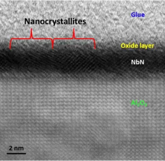
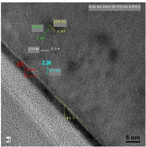
2.2.1 Transmission Electron Microscopy measurements . . . 46
2.2.2 TEM Results . . . 47
2.3 Ex-situ transport measurements . . . . 49
2.3.1 Preliminary measurements after deposition . . . 49
2.3.2 Detailed magneto-transport experiments . . . 50
2.3.3 Resistance evolution as a function of film thickness . . . 50
2.1
Sample elaboration
The samples were elaborated in Germany by our collaborators at the KIT1. The same
thin films of NbN are lithography processed and patterned in KIT to form single photon detectors [SGB+09].
2.1.1 Substrate
Al2O3 sapphire substrates which crystallographic structure is hexagonal were used.
This substrate was chosen because it is a very good thermal conductor and an excellent electrical insulator. Indeed, for single photon detectors, based on a superconducting NbN meander, it is crucial to have an insulating substrate to avoid inverse proximity effects. High thermal conductivity is advantageous to rapidly relax the detector after photon count into its "wait" state, thus increasing the detector’s counting rate. In order to study a system as close as possible to this device, we kept the same Al2O3 substrate. Besides,
it provides a particular lattice mismatch between the substrate and the NbN layer due to the R- plane surface orientation (see figure 2.1). That determines among others the structural properties of the NbN films.
Substrates were chemically cleaned before depositing the NbN layer. The purpose of this process is not to obtain a reconstruction of the surface of sapphire but to remove impurities. Moreover, before depositing, substrates are annealed. This step enables the elimination of water molecules present on top of the substrate, thus avoiding the formation of Nb-O links at the NbN-Al2O3 interface.
Figure 2.1: Sapphire unit cell showing the possible orientation of the surface. The substrate
used to deposit NbN films are R-plane oriented.
2.1.2 Vacuum deposition
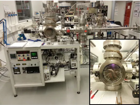
NbN thin films were grown ex-situ by DC reactive magnetron sputtering [KA00]. The apparatus used in the Karlsruhe Institute of Technology can be seen on figure 2.2. Before
![Figure 1.7: Experimental phase diagram of homogeneously disordered films drawn by [FIKC10].](https://thumb-eu.123doks.com/thumbv2/123doknet/14493453.717994/28.892.191.683.117.418/figure-experimental-phase-diagram-homogeneously-disordered-films-drawn.webp)
![Figure 1.9: Color map of the spatial inhomogeneities of the gap measured by STS in TiN and extracted from [SCB + 08].](https://thumb-eu.123doks.com/thumbv2/123doknet/14493453.717994/30.892.220.670.578.878/figure-color-spatial-inhomogeneities-measured-sts-tin-extracted.webp)
![Figure 1.11: Evolution of the superconducting inhomogeneities over the sample area as a function of temperature in epitaxial NbN film with a Tc of 2.9K extracted from [KDG + 13].](https://thumb-eu.123doks.com/thumbv2/123doknet/14493453.717994/32.892.161.731.111.667/figure-evolution-superconducting-inhomogeneities-function-temperature-epitaxial-extracted.webp)
![Figure 1.16: Left: Magnetoresistance peak measured on epitaxial NbN film extracted from [CMK + 12]](https://thumb-eu.123doks.com/thumbv2/123doknet/14493453.717994/36.892.142.750.119.362/figure-left-magnetoresistance-peak-measured-epitaxial-nbn-extracted.webp)
![Figure 1.17: Schematic representation of the three models used by [SGP + 14] to described the superconductor-insulator transition in InO films](https://thumb-eu.123doks.com/thumbv2/123doknet/14493453.717994/37.892.155.734.111.313/figure-schematic-representation-models-described-superconductor-insulator-transition.webp)