HAL Id: tel-01142084
https://tel.archives-ouvertes.fr/tel-01142084
Submitted on 14 Apr 2015
HAL is a multi-disciplinary open access archive for the deposit and dissemination of sci-entific research documents, whether they are pub-lished or not. The documents may come from teaching and research institutions in France or abroad, or from public or private research centers.
L’archive ouverte pluridisciplinaire HAL, est destinée au dépôt et à la diffusion de documents scientifiques de niveau recherche, publiés ou non, émanant des établissements d’enseignement et de recherche français ou étrangers, des laboratoires publics ou privés.
nanowire based junctions
Chuan Li
To cite this version:
Chuan Li. Superconducting proximity effect in graphene and Bi nanowire based junctions. Mesoscopic Systems and Quantum Hall Effect [cond-mat.mes-hall]. Université Paris Sud - Paris XI, 2014. English. �NNT : 2014PA112361�. �tel-01142084�
Discipline : Physique des Solides
Thèse de doctorat
Soutenue le 26 novembre 2014 par
Chuan Li
Superconducting proximity effect in
graphene and Bi nanowire based junctions
Directrice de thèse : Mme. Sophie Guéron Directrice de recherche (LPS, CNRS)
Composition du jury :
Président du jury : Pascal Simon Professeur (LPS, Univ. Paris-sud) Rapporteurs : Christoph Strunk Professeur (Rengensburg University)
Claude Chapelier Ingénieur (INAC CEA)
Examinateurs : Alexander Brinkman Professeur (University of Twente)
Behnia Kamran Directeur de recherche (ESPCI)
and Bi nanowire junctions
a dissertation presented by
Chuan Li to
The Department of Physic
in partial fulfillment of the requirements for the degree of
Doctor of Physics in the subject of Condensed matter University of Paris Sud
Orsay, France November 2014
1 Introduction 13
2 Theoretical concepts 29
2.1 Proximity effect . . . 30
2.2 Graphene . . . 45
2.3 Spin-orbit coupling . . . 56
2.4 Bismuth and SOC . . . 57
3 Superconducting proximity effect in S/G/S junction 69 3.1 Sample description and characterization . . . 70
3.2 Sample in short junction limit . . . 73
3.3 Samples in long junction limit . . . 73
3.4 Diffusive SGS junction from short junction to long junction limit . . . 86
3.5 Proximity effect in the integer quantum Hall regime . . . 88
3.6 Conclusion . . . 93
4 Superconducting proximity effect in molecule grafted graphene 95 4.1 Sample preparation . . . 97
4.2 Charge transfer between graphene and porphyrins: Neutralization of graphene by porphyrins . . . 98
4.3 Low temperature magneto-transport of functionalized samples with normal elec-trodes: asymmetry of the magnetoresistance . . . 101
4.4 Samples with superconducting contacts . . . 103
4.5 Discussion . . . 114
4.6 Conclusion . . . 117
5 Superconducting proximity effect in Bismuth nanowire 119 5.1 Proximity effect in Bismuth nanowire at zero field . . . 121
5.2 Field dependence of critical current . . . 123
5.3 discussion . . . 128
5.4 Conclusion . . . 132
A.2 Pt-porphyrin molecules . . . 145 A.3 Bi nanowire . . . 145 A.4 Superconductivity of the ReW electrodes . . . 149
Appendix B Supplementary transport measurement 153
B.1 Highly disordered graphene and indication of a gap opening . . . 153
remercier de nombreuses personnes du laboratoire.
Je tiens tout d’abord à remercier grandement l’ensemble du groupe MESO qui m’a accueilli avec beaucoup d’enthousiasme depuis 3 ans. Surtout Hélène et Sophie. Comme notre professeur de cours de Physique mésoscopique en M2, Hélène m’a amené au monde du « MESO ». Je suis com-plètement étonnée par sa passion de la physique et son humour incroyable de physicienne. Avec elle, on a non seulement fait les expériences mais on s’est vraiment amusé avec la physique. Sophie m’a appris les expériences pas à pas, m’a expliqué de façon claire et concise, m’a assuré à chaque étape et jusqu’à ce que je puisse manipuler comme une « grande ». J’ai bénéficié de toutes les discussions, les blagues, les bavardages qu’on a eu dans les bureaux, dans la salle de manips, pendant la pause-café, à la descente de la colline, ou même dans le train, dans la voiture… Ces innombrables moments changeaient petit à petit ma vie et ne disparaîtront jamais. Une preuve de ça est que je resterai « difficile » comme vous quand il s’agit de la physique.
Sandrine m’a beaucoup aidé (presque chaque fois) sur les cryostats et la dilu. Sans elle, il m’était apparu toujours long et difficile de trouver ce que je voulais. Je veux remercier Richard pour ses solutions efficaces et optimisées à tous genres de problèmes. Son attitude rigoureuse en recherche et le travail nous montre un modèle à suivre. C’est aussi un plaisir de discuter avec lui sur les points scientifiques et quotidiens. Alik est toujours un ami très encourageant. J’apprenais souvent de nou-velles choses quand je discute avec lui. Sa technique incomparable a renforcé nos expériences lors de tous les moments importants. I like the ‘crazy ‘ experiments that we did.
Merci à Bastien pour l’accompagnement vivant pendant ces 3 ans (presque). Quand j’essayais de préparer l’album de photo pour ton départ du labo, je me suis rendue compte qu’on a passé vraiment pas mal de temps ensemble ! Pour te récompenser pour les petits cours de Français mélangés avec tes blagues dures, j’ai fait aussi des efforts pour te donner un nom chinois propre. Comment on arrivait à supporter l’autre ?
J’espère que j’ai laissé une impression quand même correcte à Raphaëlle et Anil, nos nouveaux et intelligents thésards du groupe, pendant la dernière année. J’apprécie beaucoup les soirées qu’on a passées aux restaurants ou à la maison. Ça ne vous fait pas trop peur la nourriture chinoise ? Je vous remercie pour m’avoir aidé à préparer ma soutenance. Surtout Raphaëlle a bien « occupé » mes parents ! Je vous souhaite une très bonne continuation.
I would like to thank Katsuyoshi and Shamashis, our post-docs each assisted the beginning and last year of my thesis. With you, I spent much pleasant time in both scientific discussions and casual chats. Also many thanks to Katsuyoshi for the beautiful pictures at every New Year!
Aussi merci à Meydi et Alexei pour m’aider quand j’ai eu besoin et pour m’encourager aux mo-ments importants de loin et de près.
cussion des petits monstres se lançaient pendant les pauses.
En dehors du groupe, au labo j’ai une liste longue de personnes à remercier. Merci à Raphaël pour ses aides irremplaçables. Je l’ai beaucoup embêté avec des bagatelles. Je veux exprimer mes remerciements sincères à M. Claude Pasquier, qui m’accueilli sympathiquement la première fois au sein du groupe haute pression de ce labo quand je venais d’arriver en France. C’est un souvenir spécial pour moi. Il m’a toujours aidé quand j’en ai eu besoin, jusqu’à la veille de ma soutenance. Merci à M. Pierre-Antoine Albouy pour ses sourires encourageants pendant tous ces années au labo. Merci à M. Michel Héritier pour m’avoir aidé et encouragé pendant le M2. Merci à Mme. Hélène Raffy pour nous conseiller sur l’expérience et pour les communications en chinois aux occasions.
Je dois remercier mes amis doctorants du labo. Julien, en dehors de ses soirées sympathiques et ses BDs immanquables, il m’a aidé souvent sur les procédures administratives compliquées.
Beaucoup de remerciements à mes amis chinois à Paris. Merci à Lukui, pour m’avoir accueilli et supporté.
Je veux remercier mes amis du club de tennis de table à Fresnes. Merci pour vos accompagne-ments, encourageaccompagne-ments, et soutiens.
En dernier, je remercie toujours du fond du cœur mes parents, même si ça ne suffira jamais. Je vous aime.
Résumé
Introduction
L’effet proximité de supraconductivité (EPS) est un probe sensible à la cohérence, propriété de spin, même le magnétisme des systèmes. Cet effet est profondément étudié depuis centaine années dans les systèmes variés (isolateur, métal normal, semi-conducteur, matériaux ferromagnétiques, etc..) et parfois combiné avec les autres effets (l’effet Hall quantique, couplage spin-orbite, interaction électron-électron, etc..).
Dans cette thèse, nous sommes intéressés par EPS dans deux systèmes particuliers : graphène et nanofil de Bismuth. Nous allons montrer que le EPS est un outil puissant à sonder et relever les physiques dans les systèmes différents. Parfois, la compréhension du EPS est améliorée par la combinaison avec ces effets.
D
epuis la découverte du graphène en 2005, beaucoup d’effort est fait sur ce matériau 2D na-turel. La relation dispersion linéaire à l’énergie basse ouvre la porte à la physique Dirac[1,2]. La densité de charge modulable (même la signe de charge) nous permet de changer les paramètres physiques à un échelle beaucoup plus grand dans un seul système. En conséquence, au champ mag-nétique relativement bas, l’effet Hall quantique peut être observé[3,4,5,6].Non seulement la densité de charge, mais aussi les propriétés électroniques sont modulables dans graphène. En changeant une tension de grille, on peut tester l’effet proximité dans les jonctions S/G/S aux régimes différents. Nous avons examiné les jonctions diffusives courtes et longues et comparé le produit eRNIcaux différentes échelles d’énergies (le gap supraconducteur, l’énergie de
Thouless,…).
La réflexion Andreev ordinaire à l’interface S/N pour la conversion d’un pair de Cooper à un pair de quasi-particule d’électron-trou (ou vice versa) devient une réflexion spéculaire si le niveau de Fermi est ainsi proche au point Dirac[7]. En comparant le courant critique des jonctions S/G/S dif-férentes, nous trouvons que la réflexion Andreev spéculaire est relevé indirectement[8] (Sec.3.3.2).
L’injection des pairs de Cooper aux canaux balistiques 1D
Après la première observation du contact normal atomique quantique (NQPC pour l’anglais nor-mal quantum point contact), l’injection des pairs de Cooper à un canal balistique devient possible. Ce système est étudié théoriquement par Beenakker et van Houten[9] et un courant critique quan-tifié pour N modes occupées est donné :
ΔIc =
T e
4πτ, (1)
si la jonction est courte (L/ξ0 → 0). Il est observé pour la première fois par Takayanagi et al.[10].
Pour le case opposite d’une jonction longue (L ≫ ξ0) balistique S-QPC-S, le courant critique
est quantifié à une valeur non-universelle
ΔIc =
T e
4πτ, (2)
oùT est la probabilité de transmission normale par l’interface N/S selon la théorie BTK[11], et τ est le temps de voyage effectif, si une barrière finie à l’interface et un mismatch de la vitesse de Fermi sont rendu compte.
Pour le gaz d’électron 2D (2DEG en anglais pour 2D electron gas), dans un champ magnétique haut, les états de bord Hall quantique qui sont aussi les canaux balistiques 1D, sont établis. L’injection des pairs de Cooper est aussi considérée théoriquement[12] et tentée expérimentalement[13, 14]. Contrairement à la jonction S-QPC-S, la jonction S-QHS-S n’a pas montré un supercourant. Le
tique relativement bas (∼4T). Comme les contacts ohmiques sont meilleurs sur graphène que sur le 2DEG [15,16], la prospective d’injecter des pairs de Cooper au canaux des états de bords d’Hall quantique parait plus favorable. Il est un des buts de cette thèse, et sera discuté dans la chapitre 3.
L’intérêt du couplage spin-orbite
Le couplage spin-orbite (SOC pour l’anglais spin-orbit coupling) couple le degré de liberté du spin d’un électron à son mouvement orbital. Dans certains systèmes, le SOC peut être modulé par un champ électrique externe, ainsi offre une méthode pratique de contrôler le spin[17]. Un rôle impor-tant à cet effet peut être espéré pour le SOC dans le sprintronique. L’effet du SOC est aussi lié à la supraconductivité triplet. Par exemple, Gor’kov et al. a montré que le SOC Rashba peut conduire au mélange des appariements singlet et triplet dans le système supraconducteur 2D[18].
Beaucoup des études sont faits pour combiner la supraconductivité (induite) avec le SOC. Il con-duit à une transition 0− π[19,20] ou un splitting du spin du niveau Andreev dans certaines jonc-tions Josephson[21]. Même la formation des fermions Majorana est prédite[22,23] et observée[24] dans les fils quantique avec un SOC fort.
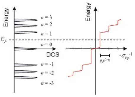
Un autre effet spectaculaire dérivé du SOC est l’effet spin Hall quantique (QSHE pour l’anglai quantum spin Hall effect) )[25]. Le QSHE engendre la conductance quantifiée en l’absence de champ magnétique, donc sans brise la symétrie reverse du temps. Les niveaux de Landau sont créés par le SOC. La différence entre le QSHE et le QHE est que la chiralité dépend de la direction du spin, i.e. les charges sont polarisés en spin quand ils propagent dans une direction et polarisés en direction du spin opposée quand ils propagent dans une autre direction.
Dans cette thèse, nous sommes intéressés à induire l’effet proximité de supraconductivité dans des systèmes différents avec un SOC (intrinsèque ou induit). Les concepts basiques sur le SOC sont décrites dans la section 2.4.
Induire le couplage spin-orbite dans graphène
Le petit SOC intrinsèque dans graphène empêche la formation d’un état isolant topologique dans le graphène. [26,27]. Beaucoup de méthodes sont proposées à induire le SOC dans graphène pour les intérêts tous les deux dans spintronique (graphène a un temps de relaxation du spin très long) et les autre recherches fondamentales. La déposition des atomes sur graphène est théorique-ment prédit à induire le SOC[28]. Une version similaire est la déposition des métallo-molécules
organique dans lesquels un atome métallique est encerclé par des molécules organiques cycliques. Plusieurs molécules sont prouvés d’apporter un moment magnétique quand ils sont ionisés[29,30,
31,32]. Nous utilisons les Pt-porphyrines dissous dans le solvant THF à fonctionnaliser graphène, espérant que les molécules se forment un arrangement ordonné sur graphène et induisent le SOC dans graphène par l’atome Pt.
Fort couplage spin-orbite dans Bismuth
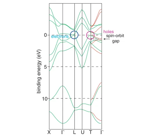
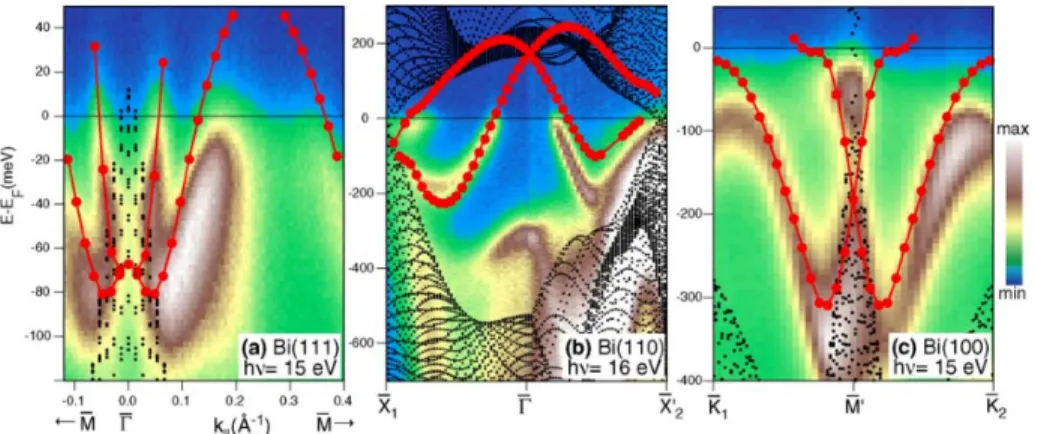
Bismuth est un semi-métal avec fort couplage spin-orbite. Un grand nombre d’études sont effec-tués pour déterminer la structure de bande dans le bulk, surface (film mince) et nanofil[33,34,35]. Les mesures de photoémission à angle résolu (ARPES pour l’anglais Angle-resolved photoemission) [36,37] et de STM (scanning tunneling microscope) [38] montrent que les états de surface se for-ment sur certaines facettes du cristalline de Bismuth (e.g. [111]). Les propriétés des états de surface sont complètement différentes que celles de bulk : densité de charge plus grande, longueur d’onde de Fermi plus petite et plus important, une splitting de spin dans la structure de bande due à la brise de la symétrie inversion. Dans les nanofils de Bismuth, le confinement quantique favorise la contri-bution des états de surface. L’état spin Hall quantique est aussi prédit théoriquement pour la facette [111] [39]. Les fils de Bismuth de bonne qualité sont mesurés pendant cette thèse. Ils fournissent un plate-forme pour le mesure de transport balistique.
Cette thèse
Cette thèse est en 5 chapitres : dans le premier chapitre, nous décriront les concepts théoriques importants. Il est principalement sur l’effet de proximité de supraconducteur, ainsi le graphène et Bismuth. Les chapitres 3 et 4 sont sur les jonctions de graphène et graphène fonctionnalisé. Ils sont fortement liés, en ce sens qu’ils partagent les mêmes échantillons mesurés avant et après la déposition des molécules. Dans le chapitre 5, nous montrons les résultats sur les jonctions de nanofils de Bi. Due au couplage spin-orbite très fort, l’effet de proximité de supraconducteur est beaucoup modifié. A partir de ces effets, nous déduiront les propriétés exotiques dans les nanofils de Bi.
1. Effet de proximité supraconducteur dans graphène
Le diagramme complet de eRNIcvs EThdans les jonctions S/G/S diffusives
Avant cette thèse, la supraconductivité induite dans graphène est réalisée par plusieurs groupes[40,
41,42]. Par contre, les échantillons, malgré tout, sont plus tôt dans le régime de la jonction courte (L. ξs). Nous avons réussi à fabriquer les échantillons avec les contacts différents ainsi les longueurs
10-3 10-2 10-1 10-4 10-3 10-2 10-1 100 101 102 103 RnIc_MC RnIc_NC RnIc_PM_porph RnIc_NC_porph RnIc_MC_porph RnIc_Nb RnIc_ReW
eR
NI
C/∆
E
Th/∆
Theory Theory renormalizedFigure 0.0.1: Relation normalisée de RNIc−EThdes jonctions S/G/S Les différentes couleurs
correspondent aux échantillons différentes. Les données expérimentales sont 3 – 100 fois plus petites que la théorie. Quelques échantillons correspondent à
ETh/Δ≈ 1 sont dans la limite intermédiaire. La jonction plus longue PM, qui
cor-respond à une courbe plate dans la régime de la jonction courte. Les échantillons Nb et ReW sont proportionnels à ETh dans la régime de la jonction longue.
pour que les échantillons se trouve dans un grand régime, puis compléter le diagramme de l’effet de proximité supraconducteur dans graphène. Quand on compare le courant critique experimental à la théorie pour une interface parfaite, une réduction existe toujours [40,42,41]. Selon notre dia-gramme d’effet de proximité (Fig.1.0.1), le facteur de réduction dépend la limite de jonction : il est près que constant dans la régime de la jonction courte, et décrois rapidement quand il entre dans le régime intermédiaire, et la régime de la jonction longue.
L’indication de la réflexion Adreev spéculaire (SAR pour l’anglais Specular An-dreev Reflection)
Dans les jonctions longues, nous avons observé une suppression inattendue du supercurrent près du point Dirac, qui doit être robuste dans une jonction courte malgré la présence des puddles de charge. En excluant l’effet thermal et la transmission finie comme l’origine de cette suppression, nous pensons c’est une indication de la réflexion Andreev spéculaire (Fig.1.0.2).
0.1 1 10 100 -20 0 20 IC JN IDC (nA ) 𝛼 ⋅ 2.08Δ/𝑅𝑁 VG(V) 0.1 1 10 100 -30 -20 -10 0 10 IDC (nA ) VG(V) 𝛼 ⋅ 10.82E𝑇ℎ/𝑅𝑁 IC Nb 𝛼 = 0.11 𝛼 = 0.024
Figure 0.0.2: Ic théorique et mesuré des échantillons JN (Ti/Al) et Nb (Pd/Nb). (gauche) JN
est dans la limite de la jonction courte, (droit) Nb est dans la limite de la jonction longue. Tous les deux a un courant critique plus petit que la théorie. Autour du point Dirac, Icde Nb décroit beaucoup plus rapide que Icde JN.
L’injection des pairs de Cooper dans le régime Hall quantique
L’interaction d’effet de proximité supraconducteur et l’effet Hall quantique est étudiée dans cette thèse. Un graphène feuille contacté par deux électrodes supraconducteurs haut Hcest une
configu-ration possible à injecter les pairs de Cooper dans les canaux quantifiés Hall quantiques. L’effet Hall quantique est caractérisé by une conductance quantifiée avec un facteur de remplissage entier ν qui correspond aux niveaux de Landau. Dans le graphène, ce facteur est décalé par un demi-entier.
σ = ge 2 h (n + 1 2) = 4e 2 h (n + 1 2) (3)
Nous avons réussi à connecter le graphène par les contacts de ReW qui a un champ critique Hc∼
8T. Sur les plateaux, les courbes dV/dI(IDC)ont toujours un peak à IDC = 0 et en revanche, entre
deux plateaux, parfois nous trouvions des creux à IDC = 0 (Fig.1.0.4). C’est une indication de la
Figure 0.0.3: La résistance différentielle en fonction la grille d’échantillon ReW au champ
mag-nétique de 0 à 7.5T. T=70mK. L’inséré montre comment le plateau Hall à 7.5T et VG= 14V évolue quand la température augmente.
8 4 0 -4 -1 -0.5 0 0.5 1 IDC(µA) VG (V ) 1 2 3 4 2.80 3 2.75 2.70 2.65 2.60 -1.0 -0.5 0.0 0.5 1.0 2 2.36 2.32 2.28 -1.0 -0.5 0.0 0.5 1.0 1 2.30 2.25 2.20 2.15 -1.0 -0.5 0.0 0.5 1.0 4 3.10 3.08 3.06 3.04 3.02 3.00 -1.0 -0.5 0.0 0.5 1.0 IDC(µA) dV /dI (k Ω ) dV /dI (k Ω ) dV /dI (k Ω ) dV /dI (k Ω ) 3.0 2.8 2.6 2.4 2.2 dV/dI (kΩ) B = 7.5T Plateau
Figure 0.0.4: La résistance différentielle d’échantillon ReW à 7.5T pour les tensions de grille.
Gauche : 2D-plot de dV/dI(IDC(nA)) pour les tensions de grilles différentes (y axe).
La courbe rouge est le profil de la résistance différentielle à IDC = 0 Droit: les
profils pour les dV/dI(IDC) courbes à certaines tensions de grilles (lignes noires).
2.Effet de proximité supraconducteur dans le graphène
gr-effé par les Pt-porphyrines
L’échange entre les métallo-porphyrines et graphène est associé à la formation d’un singlet mangé-tique délocalisé dans les molécules, indépendant à la nature de cet atome métallique. Nous étudions les modifications des propriétés de transport à basse température dans les jonctions de graphène avant et après la déposition des Pt-porphyrines.
Neutralisation de graphène : transfert de charge
Des dépostions similaires sont faites avant cette thèse [43, 44] et le spectroscope Raman d’une molécule sur graphène implique un dopage de charge dans graphène. Les molécules différentes sont sensée d’être soit un donneur soit un accepteur. Mais d’après notre mesure de transport, nous trouvons une neutralisation de graphène due à un transfert de charge(Fig.1.0.5).
Dépendance de la grille du magnétisme relevé par l’effet de proximité
Le modèle basique pour étudier la formation du moment magnétique dans un métal est le mod-èle d’impureté Anderson [45]. Basé sur ce modèle, Uchoa et al. montre que les impuretés dans
400 300 -10 -5 0 5 10 VG(V) 200 100 -20 0 20 VG(V)
Figure 0.0.5: La dépendence de la grille de résistance avant et après la déposition des
por-phyrines sur deux échantillons : (a) Nb, (b) G92TiAl_MC . Sans porpor-phyrines (bleu) les échantillons peuvent être dopé en trou (a) et en électron (b). Après la déposition, dans les deux cases, le point Dirac est ramené à zéro volte. Il implique un double sens transfert de charge.
graphène peuvent être changés de magnétique à non-magnétique en changeant le niveau de Fermi. Nous détectons ce modèle dans graphène par l’effet de proximité.
Pour les jonctions longues, nous observons que , après la dépostion de porphyrines, le super-courant devient asymétrique par rapport la grille : dans la région dopée en trou, Icest plutôt
inaf-fecté, au contraire dans la région dopé en électron, supercourant est supprimé. (Fig.1.0.9).
Nous expliquons ces résultats par une interaction RKKY de longue portée entre les molécules, via les porteurs de charge dans graphène, conduisant à un ordre magnétique collectif dans les por-phyrines.
-60 -40 -20 0 20 40 60 Vg(V) 150 100 50 0 -20 -10 0 10 20 150 100 50 0 dV /dI (Ω ) a b 100 0 dV/dI (W) 100 0 dV/dI (Ω) 100 0 dV/dI(Ω) 100 0 dV/dI(Ω)
Before putting porphyrin
After putting porphyrin 100 50 0 dV/dI(Ω) -0.2 -0.1 0.0 0.1 0.2 100 50 0 -1.0 -0.5 0.0 0.5 1.0 IDC (μ A) IDC (μ A) dV /dI (Ω ) dV/dI(Ω)
Figure 0.0.6: Da la supraconductivité induite bipolaire à unipolaire. Les régions rouges
foncées correspondent à une résistance différentielle nulle. (a) avant de mettre les porphyrines, le supercourant est bipolaire, (b) après la déposition, le supercourant devient unipolaire.
3. Effet de proximité supraconducteur dans les nanofils de
Bismuth
A basse température (100mK) et champ nul, nous arrivons à induire la supraconductivité dans les nanofils de Bi par les électrodes de tungstène. Les courant critique est entre 100nA et 1μA.
Supercourant persistent à 11T
Les électrodes de tungstène ont un champ critique très élevé (∼ 12T). Nous trouvons l’état supra-conducteur induit dans les fils de Bi jusqu’à 11T (Fig.1.0.10). C’est vraiment différent ce qu’on attend pour un fil d’or de la même taille.
Les oscillations du courant critique comme un SQUID modulées dans une grande échelle
Une oscillation comme un SQUID du courant critique de 0T à 9T et une modulation sur ces oscilla-tions d’une échelle d’1T sont observées(Fig.1.0.11).. Elles correspondent respectivement une forma-tion des états de bord 1D très confinés sur certaine surface du nanofil de Bismuth, et l’effet Zeeman.
10 8 6 4 2 dV /dI (k Ω ) -100 -50 0 50 100 IDC(nA) 5T 5.5T 6T 6.5T 7T 7.5T 8T 8.5T 9T 9.5T 10T 0 T 10 T T = 600mK
Figure 0.0.7: dV/dI coubes aux champs différents. Les courbes de la résistance différentielle
en function du courant DC sont prises aux différents champs de 0 à 11T.
6.9 B(T) 70 60 50 40
Bi1
B
⊥Bi3
B⊥𝟏T=100mK
a
b
80 75 70 IC (nA) 0.8 0.7 B(T)c
e
1.9 2.0 1.5 1.0 0.5 0.0 5 4 3 2 1 B(T) 100mK 700mK 1.2K 1.7K IC (µ A)d
I C (nA ) 80 75 70 2 1 0 B(T) IC (nA ) 15 10 5 0 dV /dI (k Ω )Figure 0.0.8: Oscillations comme un SQUID dans Bi1 et Bi3(a) and (b) montrent des
oscillations du IC en fonction du champ magnétique avec une période de 800
Gauss (a) et de 150 Gauss (b) pour l’autre;(c) est une figure zoomée sur une échelle de 2000 Gauss de (b); (d) et (e) sont les scans des courbes de dV/dI à different champs.
Introduction
The superconducting proximity effect (SPE) is a sensitive probe of the quantum coher-ence, spin properties, or even magnetism of systems in which superconducting correlations can be induced by coupling them to superconductors. This effect has been widely studied for almost 100 years in various systems (insulators, normal metals, semiconductors, ferromagnetic materials, etc...) and sometimes in combination with other effects (quantum Hall effect, spin-orbit coupling, electron-electron interaction, etc...).
In this thesis, we are interested in the SPE induced in two particular systems, graphene flakes and bismuth nanowires. We are going to show that the SPE is actually a powerful tool to probe and to reveal different physics in various systems. Sometimes, the understanding of the SPE can also be improved by combining it to other effects.
S
ince the discovery of graphene in 2005, a lot of attention has been paid to this natural 2D mate-rial. Graphene’s special band structure leads to many interesting features. The linear dispersion relation at low energy opens the door to Dirac physics[1,2]. The gate tunable carrier density (and even the sign of carriers) allows one to explore the physical parameters in a much larger range in both conduction and valence band in a single system. As a consequence, at a relatively low magnetic field, the quantum Hall effect can be observed in this natural 2D material[3,4,5,6].Not only the carrier density is tunable in graphene, but also the transport properties. By gating the sample, one can test the proximity effect in S/G/S junctions in different transport regimes: we have examined both diffusive short and long junctions system, and compared the proximity effect “figure of merit”, the eRNIc product, to the theoretical predictions that involve different energy
scales (superconducting gap, Thouless energy...).
The ordinary Andreev retro-reflection at the S/N interface for the conversion of a Cooper pair into an electron-hole quasi-particle pair (or vice versa) can become a specular reflection in S/Graphene interface when the Fermi level is close enough to the Neutrality point (or the Dirac point)[7]. By comparing the supercurrent in different S/G/S junctions, we find that the specular Andreev reflec-tion is indirectly revealed [8] (Sec.3.3.2).
The injection of Cooper pairs into ballistic 1D channels
After the first observation of normal quantum point contact (NQPC), the injection of Cooper pairs into a ballistic channel became possible. This problem was theoretically addressed by Beenakker and van Houten[9] and a quantized critical current for N occupied modes is given by
Ic = N
eΔ0
~ (1.1)
if the junction is short (L/ξ0 → 0). This was observed for the first time by Takayanagi H. et al.[10].
For the opposite case of a long (L≫ ξ0) ballistic S-QPC-S junction, the critical current is
quan-tized at a non-universal value
ΔIc =
T e
4πτ, (1.2)
whereT is the normal-transmission probability through the N/S interface according to BTK the-ory, and τ is the effective travel time, if a finite barrier at the interfaces and a Fermi velocity mismatch are considered.
For the 2DEG, in high magnetic field, the quantum Hall edge states are established, which are also 1D ballistic channels. The injection of Cooper pairs was also considered theoretically[12] and attempted experimentally[13,14]. In contrast to S-QPC-S junction, the S-QHS-S junction didn’t show a supercurrent and not even mention the critical current quantization. The trace of the
su-ture 2D electron gas[15,16], the prospect of injecting Cooper pairs into quantum Hall edge states in graphene using high Hcsuperconductor electrodes seems more favorable. That’s one of the goals
of this thesis. We are going to discuss the results in Chapter3.
The interests of spin-orbit coupling(SOC)
The spin-orbit coupling couples an electron’s spin degree of freedom to its orbital motion. In certain systems the SOC can be modulated by an external electric field, thus providing a conve-nient method of spin control[17]. An important role can therefor be expected for the SOC in the sprintronics. The SO effect is also related to triplet superconductivity. For example, Gor’kov et al. showed that the Rashba SOC can lead to the mixing of singlet and triplet pairings in 2D supercon-ducting system[18].
Much attention has been paid to combining the (induced) superconductivity with SOC. It leads to a possible 0− π junction transition[19,20] or an Andreev level spin splitting in some Josephson junctions[21]. Even the formation of Majorana fermions[22,23] is predicted and observed[24] in quantum wire with strong SOC.
Another spectacular effect derived from the SOC is the quantum spin Hall effect (QSHE)[25]. The QSHE gives rise to quantized conductance in the absence of magnetic field, thus without breaking the time reversal symmetry. The degenerate quantum Landau levels are created by the SOC. The QSHE differs from the quantum Hall effect in that the different chirality depends on the spin direction, i.e. the charges are spin polarized when they propagate in one direction and polarized in opposite spin direction when they propagate in the another direction.
In this thesis, we are also interested in inducing superconducting proximity effect in different systems with (intrinsic or induced) SOC. The basic concepts about SOC are described in Sec.2.3.
Inducing spin-orbit coupling in graphene
The intrinsic small SOC in graphene prevents the formation of a topological insulating state in graphene[26,27]. Many ways are considered to induce the SOC into graphene sheet for the in-terest both in spintronics (graphene has a very long spin relaxation time) and other fundamental researches. Deposition of adatoms on graphene has been theoretically predicted to induce SOC in graphene[28]. This can be done with a similar vision by depositing organic metallo-molecules in which a metallic atom is encircled by cyclic organic molecules. Various molecules have been proved
to carry a magnetic moment when charge transfer occurs[29,30,31,32]. In this thesis we use Pt-porphyrins in THF solvent to fictionalize graphene, the molecules are expected to constitute an ordered arrangement on graphene, with heavy Pt atoms inducing SOC in graphene.
Molecule deposition on graphene
Meanwhile, the molecule deposition on graphene is one of the approaches to controllably change the doping in graphene[46,44] which holds great application interests and also interesting physic to be explored. The fact that certain molecules serve as donors[47] or acceptors[47,44] of electrons can be understood by the simple HOMO-LUMO energy gap structure. However the bending of energy bands in molecules at the interface of molecules and metal, semi-metal, insulator is well studied in organic-semiconductor systems. Also a reduction in energy gap is observed when they interact with substrate, metal, or graphene for vast systems[48,49]. In this thesis, we find a dual direction charge transfer between graphene and molecules. A auto-alignment mechanism[50,51,
52] must be involved in this process. This may imply a more complex mechanism if the possible charge transfer in-between the molecules, like tunneling[53] or thermally activated hopping[54,55] processes, are taken into count. The determination of the origin of this charge transfer is beyond the scope of this thesis, but it will be still carefully discussed in the Appendix B.
Strong SOC in Bismuth
If one talks about spin-orbit coupling, Bismuth has to be mentioned. Bismuth bulk is a semi-metal with strong SOC. A lot of work has been done to determine the band structures in bulk, surface (thin film), and nanowires[33,34,35]. Angle- resolved photoemission (ARPES) measurements[36,
37] and very recent STM and transport measurements[38] show that surface states form on certain facets of Bi crystals (e.g. [111]). These surface states have completely different properties than Bi bulk: higher carrier density, smaller Fermi wavelength λF, and in particular spin split bands due to
inversion symmetry breaking. In Bi nanowires, quantum confinement favors the contribution of surface states compared to bulk states. The quantum spin Hall state is also predicted theoretically on the Bi [111] surface[39]. The high quality Bi crystal nanowires were measured during this thesis. They may provide the platform of the ballistic transport measurement.
Outline of this thesis
This thesis is written in 4 chapters: chapter 2 describes the important theoretical concepts and basic physics needed to understand this thesis. It is mainly about the proximity effect, with an introduc-tion on graphene and Bismuth. Chapter 3 and chapter 4 are both on the S/Graphene/S juncintroduc-tions
ples) are realized in this thesis, in Appendix A we address the sample fabrication procedures, as well as our measurement system.
1. Superconducting proximity effect in pristine graphene
The full eRNIcvs EThdiagram in diffusive S/G/S junction
Before this thesis, inducing superconducting proximity effect in graphene was proved to be possible[40,
41,42]. However experiments were all in the regime of near-short junction limit L. ξs). By
mak-ing different length samples, we investigate the superconductmak-ing proximity effect through graphene from the short/intermediate junction limit to the long junction limit thus completing the diagram of the superconducting proximity effect in graphene.
When compared to theoretical prediction with perfect interface transmission, the experimentally detected critical current is always smaller[40,42,41]. We have established a full diagram from long junction to short junction of the behavior of our samples(Fig.1.0.1), and find that this discrepancy always exists and depends on the junction limit. The reduction factor in the long junction limit is 10 times higher than that in the short junction.
The indication of specular Andreev reflection (SAR)
Particularly in the long S/G/S junctions, we observed an unexpected suppression of supercurrent near the Dirac point of graphene. In many reported experiments (for short junctions), in this regime of gate voltage, the supercurrent was shown to be robust regardless of the presence of the charge puddles. Excluding the thermal effect and finite transmission, we attribute this suppression to the specular Andreev reflection (Fig.1.0.2). The field dependence of the critical current is also investi-gated for all samples.
Injection of Cooper pairs in Quantum Hall regime
The interplay of the superconducting proximity effect and quantum Hall effect was also investi-gated in this thesis. By using superconducting electrodes with high critical field (Hc) to contact a
graphene sheet, the injection of Cooper (Andreev quasi-particle) pairs into graphene in quantum Hall regime becomes possible. This was considered as one of the ways to inject Cooper pairs into ballistic quantized channels. The quantum Hall effect is generally characterized by an quantized
10-3 10-2 10-1 100 10-4 10-3 10-2 10-1 100 101 102 103 RnIc_MC RnIc_NC RnIc_PM_porph RnIc_NC_porph RnIc_MC_porph RnIc_Nb RnIc_ReW
eR
NI
C/∆
E
Th/∆
Theory a=0.3 Theory renormalizedFigure 1.0.1: Normalized RNIc−ETh relation for SGS samples from short junction limit to
long junction limit. Same color and shape dots correspond to a same sample.
All of the RNIc products are smaller than the theory curve (black) by a factor
3 to 100. Several samples correspond to ETh/Δ ≈ 1: these samples are in the
intermediate region and should behave like short junction. The shortest sample PM, which shows flat curve at doped region, is really in short junction limit. Nb and ReW samples depend linearly on ETh with the same slope (the red curve is
0.1 1 10 100 -20 0 20 IC JN IDC (nA ) 𝛼 ⋅ 2.08Δ/𝑅𝑁 VG(V) 0.1 1 10 100 -30 -20 -10 0 10 IDC (nA ) VG(V) 𝛼 ⋅ 10.82E𝑇ℎ/𝑅𝑁 IC Nb 𝛼 = 0.11 𝛼 = 0.024
Figure 1.0.2: Theoretical and measured Icof sample JN (Ti/Al) and sample Nb (Pd/Nb). (Left)
JN sample is in the short/intermediate junction limit, (right) Nb sample is in the long junction limit. Both of them have a critical current smaller than expected. For JN, the prefactor α = 0.26 implies that the critical current is 10 times smaller than expected for short junction. For Nb sample, the factor between theoretical and experimental results is about 40. The divergence of the theoretical curve is due to the dysfunction of the capacitance model:the presence of the charge puddles result in a finite conductance at the Dirac point instead of the theoretical vanishing of the density of states in graphene.
Figure 1.0.3: Two wire differential resistance as a function of gate voltage for the sample with
ReW (H c > 7.5T), at magnetic fields from 0 to 7.5 T, every Tesla between 0 and 5 T, and every 0.5 T above 5 T. Temperature is 70 mK. The inset displays how the Hall plateau at 7.5 T and VG= 14V flattens out as temperature is increased.
conductance with an integer filling factor ν which corresponds to the Landau levels. In graphene, the quantum Hall effect is shifted by a half integer
σ = ge 2 h (n + 1 2) = 4e 2 h (n + 1 2) (1.3)
due to the electron-hole gapless band structure: the lowest Landau level is shared by the electron and the hole and there is no energy level at CNP[3,4,5,6]. The quantum Hall effect (Fig.1.0.3)is observed in all our samples. One of the samples has ReW as contacts which has a high Hcup to 8T.
We found a zero-bias conductance increase at the edge of the QHE plateaus and some dip features at zero bias of the dV/dI(IDC) curves between two QHE plateaus in contrast to the seen peak for
all curves taken on the plateaus (Fig.1.0.4). This is an indirect indication of the presence of the superconducting proximity effect.
Additionally, the third harmonic differential resistance was measured at different magnetic field, the sign of which indicates a peak or a dip feature in the dV/dI curves.
8 4 0 VG (V ) 3 4 2.80 3 2.75 2.70 2.65 2.60 -1.0 -0.5 0.0 0.5 1.0 2 2.36 2.32 2.28 -1.0 -0.5 0.0 0.5 1.0 4 3.10 3.08 3.06 3.04 3.02 3.00 -1.0 -0.5 0.0 0.5 1.0 IDC(µA) dV /dI (k Ω ) dV /dI (k Ω ) dV /dI (k Ω ) 3.0 2.8 2.6 2.4 2.2 dV/dI (kΩ)
Figure 1.0.4: Differential resistance of ReW sample at 7.5T for different gate voltages. Left
color-plot of dV/dI(IDC(nA)) for different gate voltages (y axis). The red curve
is the profile of the differential resistance at IDC= 0 Right: the profiles for the
dV/dI(IDC) curves at certain gate voltages (black lines).
2.Superconducting proximity effect in Porphyrin-grafted
graphene
Metallo-porphyrins molecules are known to interact with carbon based molecules with π orbitals, giving rise to electron or hole doping. This charge exchange between the porphyrin and graphi-tized carbon is associated to the formation of a magnetic singlet delocalized on the molecule inde-pendently of the nature of the metallic host atom, which can be not magnetic. We investigated the modification of low temperature transport properties of several graphene samples after deposition of Pt-porphyrins.
Neutralization of graphene: charge transfer
Similar molecule depositions were done before[43,44], and Raman spectroscopy implies that a charge doping occurs in the graphene. Different kinds of molecules can be either donor or acceptor. Only one experiment with STM measurement shows a possible inversed charge transfer from a Ni-trogen doping in graphene to H2TPP molecule[48]. However, the transport measurement wasn’t
carried out systematically in these experiments. Our first results about the graphene grafted with molecules shows a surprising neutralization of graphene doping due to a charge transfer(Fig.1.0.5).
600 500 400 300 -10 -5 0 5 10 R( Ω ) VG(V) Nb sample 500 400 300 200 100 R( Ω ) -20 0 20 MC VG(V) a b
Figure 1.0.5: Gate dependence of resistance before and after the deposition of porphyrins for two
samples, (a) Nb sample, (b) G92TiAl_MC. Without porphyrins (blue curves), the samples can be hole doped (a) and electron doped (b). After grafting porphyrins, in both case, the Dirac point of of graphene is brought to zero, graphene becomes neutral. This implies that charge transfer occurs between graphene and porphyrins and the molecules can be donors (a) as well as acceptors (b) of electrons.
The process can even be manipulated by an external gate.
Induced magnetism
As a consequence of the charge transfers, the molecules can be tuned to a special magnetic state. Based on this point of view, we investigated both normal contact samples and superconducting contacts samples. By measuring the magnetoresistance in both perpendicular field and parallel field, we found hysteresis in perpendicular field (Fig.1.0.6) and an asymmetric feature in parallel field (Fig.1.0.7).
Gate dependence of the magnetism revealed by proximity effect
The basic model for the study of magnetic moment formation in metals is the well-known An-derson impurity model[45]. Based on this model, Uchoa et al.[56] shows that the impurities in graphene can be tuned from magnetic to non-magnetic by just changing the Fermi level (thus the gate voltage), and vice versa. We can reveal this phenomenon thanks to the superconducting prox-imity effect that we induce in graphene.
In short junctions (with Ti/Al contacts), we find the magnetic field dependence of the critical current (Fraunhofer pattern) changes with the gate (Fig.1.0.8).
For the long junctions (sample connected to Pd/Nb superconducting electrodes), we observe that, after the porphyrin deposition, whereas the Josephson current is unaffected in the hole doped region, it is strongly quenched in the electron doped one (Fig.1.0.9). We relate this quenching of the Josephson current to the formation of magnetic moments on the ionized porphyrins. This magnetism is also revealed by a sizable hysteretic magnetoresistance in the electron doped region
160 150 140 130 R( 3000 2000 1000 0 B(G) Vg = -10V T = 70 mK 86 85 84 83 R( ) 800 600 400 200 0 B(G) Vg = +70 V T = 1 K a c d b170 160 150 140 R( 3000 2000 1000 0 B(G) Vg= 9.6 V T = 70 mK 59 58 57 56 R( ) 800 600 400 200 0 B(G) Vg= -70 V T = 1 K
Figure 1.0.6: Unipolar hysteresis in the graphene’s magnetoresistance after porphyrin
deposi-tion, at two temperatures, with a field direction perpendicular to the graphene plane. The hysteresis is quite large at positive gate voltage (electron doping, b and d) and negligible (at least an order of magnitude smaller) for hole doping (a and c),confirming the existence of a magnetic order that suppresses the supercurrent for electron doping. The anomalies at very low magnetic field correspond to the superconductivity of the contacts, and exist both in the electron and hole doped regions. The reproducible fluctuations at 100 mK are mesoscopic conductance fluctuations.
R/R 0 1.008 1.006 1.004 1.002 1.000 0.998 4000 0 -4000 B(G) S2 Vg = 30V 1 2 3 4 3 4 1.006 1.004 1.002 1.000 0.998 -4000 0 4000 B(G) 1 2 R/R 0 S2 Vg = -30V 1.004 1.002 1.000 0.998 -4000 0 4000 B(G) 2 3 4 R/R 0 S3 Vg = 30V
Figure 1.0.7: In plane field effect in sample G58. (a) Asymmetric magnetoresistance in parallel
field for S2 (with porphyrins). The curves in different colors represent the sweeping order in magnetic field. (b) magnetoresistance in parallel field for S3 (without porphyrins). 500 400 300 200 100 0 -30 -20 -10 0 10 20 30 Vg = -30V with porphyrins Vg = -26V Without porphyrins B(G) IC (nA ) 1.0 0.8 0.6 0.4 0.2 0.0 -20 0 20 -30 -10 10 30 IC / IC m a x B(G) a b Vg = 4V with porphyrins Vg = 6V Without porphyrins
Figure 1.0.8: Fraunhofer pattern of sample MC before (blue) and after (red) grafting porphyrins
at different gate voltages (a: negative values; b: positive values, normalized Ic/Imaxc
-60 -40 -20 0 20 40 60 Vg(V) 150 100 50 0 -20 -10 0 10 20 0 ) b 100 0 dV/dI(Ω) 100 0 dV/dI(Ω)
After putting porphyrin -0.2 -0.1 100 50 0 -1.0 -0.5 0.0 0.5 1.0 IDC (μ A) dV /dI (Ω ) dV/dI(Ω)
Figure 1.0.9: Change from bipolar to unipolar induced superconductivity upon depo-sition of Pt-porphyrin. Color-coded differential resistance as a function of dc
current (y axis) and gate voltage (x axis), measured with a small ac current added to the dc current. The dark red regions correspond to that of zero differential resistance where a Josephson supercurrent runs through the S/graphene/S junc-tion. Whereas the Josephson effect occurs symmetrically on both sides of the Dirac point on the pristine, uncoated sample (a, T=200 mK), it only occurs on the hole doped side (negative VG ) on the sample covered with porphyrins (b, T
= 100 mK). The curves on and to the left of the color plots are the differential resistance curves as a function of dc current, measured at gate voltages symmetric with respect to the Dirac point.
(Fig.1.0.6). It is absent in the hole doped region. This spectacular effect of the critical current in long junction sample may be due to it’s high sensitivity to magnetic field.
We explain these results by a long range RKKY interaction between the molecules, mediated by the charge carriers in graphene, leading to a collective magnetic order in porphyrins.
3. Superconducting proximity effect in Bi nanowires
At low temperature (100 mK) and zero field, we induced superconducting proximity effect in dif-ferent Bi nanowire junctions by making tungsten contacts. The critical current is between 100nA and 1μA depending on the wire resistance and contact resistance.
Persistent supercurrent up to 11T
The tungsten wires have very high critical temperature Tc ∼ 4K and high critical field Hc∼ 12T. We
16 14 12 10 8 6 4 2 dV /dI (k Ω ) -100 -50 0 50 100 IDC(nA) 0T 0.5T 1T 1.5T 2T 2.5T 3T 3.5T 4T 4.5T 5T 5.5T 6T 6.5T 7T 7.5T 8T 8.5T 9T 9.5T 10T 0 T 10 T T = 600mK
Figure 1.0.10: dV/dI curves at different field of Bi3 The differential resistance as function
of DC current curves are taken at different magnetic field from 0T to 11T at 600mK. The supercurrent is still very visible at 11T.
contrary to what is expected for the field dependence of the critical current in long nanowires which decreases on a scale of about a few hundred Gauss.
SQUID-like oscillations and large range modulation in critical current
The samples exhibit SQUID-like oscillations in critical current over a magnetic field range from 0 to 9T. In addition, the SQUID-like oscillations are modulated on a large field scale of the order of 1T (Fig.1.0.11). As predicted and measured, the strong SOC and confinement in Bi nanowires may result in the formation of particular edge states. We then attribute the SQUID-like oscillations to strong confined 1D edge states along certain facets of the nanowire, and the large scale modulation to the Zeeman effect.
6.9 B(T) 70 60 50 40
Bi1
B
⊥Bi3
B⊥𝟏T=100mK
a
b
80 75 70 IC (nA) 0.8 0.7 B(T)c
e
1.9 2.0 1.5 1.0 0.5 0.0 5 4 3 2 1 B(T) 100mK 700mK 1.2K 1.7K IC (µ A)d
I C (nA ) 80 75 70 2 1 0 B(T) IC (nA ) 15 10 5 0 dV /dI (k Ω )Figure 1.0.11: SQUID-like oscillations of Bi1 and Bi3(a) and (b) show direct IC
measure-ment as function of field for Bi1 and Bi3 with a period of about 800 Gauss(a) and 150 Gauss(b) respectively;(c) is the zoom figure of 2000 gauss rang of (b); (d) and (e) are scans of dV/dI curves at different range of magnetic field, show the persistent oscillations
Theoretical concepts
How does superconducting Proximity effect happen? Andreev bound states play the role of intermediate states between two superconducting electrodes linked by a normal metal or an insulator. How does it change when a magnetic field is applied?
2.1 Proximity effect
T
he proximity effect describes the phenomena that a occur when a superconductor (S) is placedin contact with a non-superconductor (”normal metal”, N), and superconducting properties are induced in the N due to the propagation of correlated particles from the superconductor to the normal metal. This can lead to a zero resistance if the normal part is connected to two super-conductors (SNS junction). This phenomenon was first described theoretically by Josephson, and is named the Josephson effect. This effect manifests itself in a non-dissipative dc current flowing through the Josephson junction at zero voltage. At weak coupling, e.g., in the S-I-S case where a thin insulator separates the two superconductors, the Josephson current can be expressed as Is = Icsin δ,where δ is the phase difference between the two superconducting condensates and the maximum supercurrent Icis called the critical current.
We first describe the S-I-S junction, then show how the proximity effect is changed when a normal metal replaces the insulator as a coupling material. In particular, we discuss the Andreev bound states (ABS) that carry the supercurrent.
2.1.1 DC and AC Josephson effect[57]
The simplest way to understand the existence of a supercurrent is to include a coupling K between the two S wave function , each with their own phase θi. Suppose we have a SIS junction. We define
Ψ1and Ψ2as the quantum mechanical wavefunction of the superconducting state in the left and the
right superconductor, respectively. The dynamics of the two wavefunctions are then determinated by the following coupled Schrödinger equations:
i~∂Ψ1
∂t = μ1Ψ1+ KΨ2
i~∂Ψ2
∂t = μ2Ψ2+ KΨ1
(2.1)
where K is a constant representing the coupling across the barrier and μ1, μ2are the lowest energy states on either side.
In a simple way the wavefunctions can be written as Ψ1= √ n1eiφ1 Ψ2= √ n2eiφ2 (2.2)
− ~∂
∂t(φ2− φ1) = μ2− μ1
(2.3)
Let’s check the transport properties in this structure. The time derivative of the density of the Cooper pairs describes a current and thus I = ∂n1
∂t. If a voltage V is applied between the junctions
the energy levels will shift by μ2− μ1= 2eV. Then we get
I = I0sin φ DC (2.4)
∂φ ∂t =
2eV
~ AC (2.5)
By writing I0= 2K√n1n2/~ and φ = φ1− φ2. Equations (2.4) and (2.5) represent the main results
of the general theory of the Josephson junction. Eq. 2.4shows that at zero bias, a non-dissipative (DC) supercurrent flows through junction modulated by the phase difference between two super-conductor electrodes. Once one applies a voltage bias V at the two sides of the junction, the phase difference δ varies with a frequency2eV
h , induces a same frequency AC supercurrent in the junc-tion. These are the so-called DC and AC Josephson effect. This strong non-linear current-voltage behavior is the origin for many different physical phenomena.
2.1.2 Andreev reflection
Because of the existence of an energy gap at the Fermi energy in the density of states of the supercon-ductor, the transfer of single quasi-particle states with an energy ε below the gap Δ is forbidden for a direct transfer of charge. However, another type of transfer is possible when higher order processes are allowed. Andreev showed [58] that an incoming electron can be transferred into the supercon-ductor if a second electron is also transferred through the interface thus forming a Cooper pair into the superconductor. In terms of single excitations, this process is equivalent to the reflection of a hole(Fig.2.1.3).
NS interface: retro-reflection
When an incident electron arrives at the NS interface, a hole will be reflected back with an opposite motion. This curious feature was noticed by Andreev. It was observed in particular by Benistant et al. [59] in an experiment with a pure silver single crystal. The Andreev reflection is a perfect retro-reflection only for electrons incident at the Fermi energy. When the energy is above the Fermi
a
b
SS
Ψ
1= 𝑛
1𝑒
𝑖𝜙1N
I
SS
Ψ
1= 𝑛
1𝑒
𝑖𝜙1SS
Ψ
2= 𝑛
2𝑒
𝑖𝜙2SS
Ψ
2= 𝑛
2𝑒
𝑖𝜙2SS
Ψ
1= 𝑛
1𝑒
𝑖𝜙1N
SS
Ψ
2= 𝑛
2𝑒
𝑖𝜙2c
Figure 2.1.1: Josephson junctions. (a) Weak link Josephson junction (S-I-S), different phases
in two electrodes. (b) Ballistic SNS junction. (c) Diffusive SNS junction. The coherent quasi-particles pair has same trajectories with time reversal symmetry.
E
F kx ε h e kx vx h F - kF+∆k/2 kF+∆k/2e
h
N SFigure 2.1.2: Retro-reflection at the N/S interface. An electron at kF+ δk/2with a excitation
energy of ε above the Fermi energy εF will be reflected as a hole at−kF+ δk/2
with an energy of εF− ε. a) one dimensional case b) two dimensional case.
energy[60], the incident electron (EF + ε,kF + δk/2) and the reflected hole (EF − ε, −kF + δk/2)
have different wavelengths in the normal metal. The wavevector mismatch is linear in energy : δk = 2ε/~vF(Fig. 2.1.2). The Cooper pair has energy 2EF, so that the energy is conserved. Incident and
reflected quasiparticles have approximately equal wave vectors but opposite direction of motion (as follows from the opposite sign of the group velocity ε/~dk for the electrons and holes). Momentum is conserved up to the terms of order~ ke− kh . ~/ξ
0, with ξ0≡ ~vF/πΔ0the superconducting
coherence length[61]. Once a hole is reflected, it can catch a phase at the interface: η = Φ + arccos(ε/Δ), where Φ is the phase of the superconductor.
This retro-reflection occurs in most cases, but as we will show further, another, so called specular, reflection can occur at S/graphene interface.
SNS junction - Andreev Bound state (ABS)
In an SNS junction, the Andreev reflection occurs at the two NS interfaces. These reflections impose phase dependent boundary conditions on the eigenstates in the N region which are coherent super-position of electron and hole wave functions. In another word, standing waves will be formed in the normal part and lead to a quantization of excitation energy levels. We call these standing waves as “Andreev bound states (ABS)”.
2∆
e
h
z
z=0
z=L
NFigure 2.1.3: Andreev bound state. An Andreev pair formed with an electron and a hole is
confined in between the energy of±Δ. They require the constructive interference between the electron and the hole. Inspired from [63]
ballistic region of length LN[61]:
Δ(rrr) = Δ0eiφ1, if z < 0 0, if 0 < z < LN Δ0eiφ2, if z > LN (2.6)
The bound states for ε < Δ0 may be found by equating the phase shift acquired on a single
round trip to an integer multiple of 2π. The resulting condition is [58,62] 2εLN ~vFcos θ − 2 arccos ε Δ0 ± Δφ = 2πm m = 1, 2, ... (2.7)
where Δφ ≡ φ1 − φ2 ∈ (−π, π) and θ is the angle with the normal to the N/S interface. The ± sign corresponds to the two directions of motion of the electron (or hole). For ε ≪ Δ0 the
spectrum depends linearly on δφ, according to ε = [(2m + 1)π∓ Δφ] ~vFcos θ/(2LN)(Fig.2.1.3).
The first term is the phase cumulation during the propagation in the normal part, 2Δk· LN/cos θ.
The second term comes from the Andreev reflection at the interface.
sensi-Figure 2.1.4: Spectrum of Andreev bound state. a) Short ballistic junction with (solid) and
without (dotted) the presence of impurity (From Ref.[65]). b) Long ballistic junction. The discrete Andreev levels are shown with (solid) and without (dashed) the presence of an impurity. In both (a) and (b), an energy gap is opened in this quasi-particle spectrum. (From Ref.[65]).
tively on LN. The Josephson current is a linear function of Δφ with a critical current given by
Ic = αG~vF/eLNwhere α is a numerical coefficient of order unity (dependent on the
dimension-ality of the system) and G is the normal state conductance of the SNS junction (Fig. 2.1.4b). The dependence of Icon the junction geometry (through LN) is characteristic of the case LN ≫ ξ0, and
persists if the SNS junction contains a constriction of the normal region.[64]
Short junction limit:In the opposite limit LN ≪ ξ0, only a single bound state for each of the
N transverse modes remains, at energy ε = Δ0cos(Δφ/2) independent of LN (Fig. 2.1.4a). The
supercurrent is given by the sum of the contribution of the energy levels. This result implies a zero-temperature Josephson current
I(δφ) =∑ n fnin, in =− ∂εn ∂φ =−N2e ~ dε dδφ = Ne ~Δ0sin(δφ/2) − π < δφ < π (2.8)
and critical current
Ic= N
e
~Δ0 (2.9)
Multiple Andreev Reflection (MAR)
If one applies a small voltage bias between the two superconducting electrodes, the junction is in the non-equilibrium state, and there is no more supercurrent. However, another consequence of the Andreev reflection can be observed. As shown in Fig.2.1.5(c) and (d), multiple reflection of the quasi-particles can happen at all small bias voltage below the gap. Once the integer times of the bias energy neV is equal to the gap 2Δ, because of the high density of states near the gap, an enhanced conductance can be observed. This is so-called multiple Andreev reflection (MAR). With this effect we can determine the gap in our samples.
The consequences of Andreev reflection on the current voltage characteristics of a S-N junction were studied in detail in the so-called BTK theory[11]. The barrier strength was characterized by a simple parameter Z ranging from 0 for a perfect metallic contact to∞ for a low transparency tunnel barrier. With this definition, the transparency reads t = 1/(1 + Z2). The Andreev process
is significant when the transparency of the barrier is high. For a perfect contact (Z = 0) the sub-gap conductance was found to be twice the normal state conductance thus demonstrating the double charge transfer.
Diffusive SNS junction
Disorder changes strongly the ABS spectrum by lifting the degeneracies. The spectrum becomes quasi-continuous (see Fig. 2.1.6), with several striking features: a gap is induced in the spectrum which is modulated by the phase difference δφ. It closes at δφ = π. The amplitude of the induced gap depends on the junction length: in the short junction limit (L≪ ξs), it equals to the gap Δ; in
the long junction limit (L≫ ξs), because another characteristic energy, so-called Thouless energy is
involved to the system due to the disorders, there is an induced mini-gap (3.5ETh ≪ Δ) inside the
normal metal.
The transport properties in a diffusive metal can be described by a diffusion characteristic time τD =
L2
D in which electrons can travel through the metal and ”feel” the edges (D is the diffusion constant of the metal). Then the characteristic energy, Thouless energy, is given by ETh =
~ τD
= ~D
L2 . In different limits, the characteristic energies (ETh, Δ, ET = kBT) have different scales, and the
properties of the a SNS junction are changed depending on these energies.
At sufficient low temperature, ET ≪ ETh, Δ, the thermal effect is very small. The
supercon-ducting coherence length in a diffusive junction is given by: ξs =
√ ~D
Δ . By considering different energy scales, the SNS junction can be placed from short junction limit (Δ≪ ETh, ξs≫ L) to long
junction limit (Δ ≫ ETh, ξs ≪ L). Ferrier et al. calculated the ABS spectrum (Fig. 2.1.6) of short
2∆ e e 1e eV ≥ 2∆/1 e 2∆ e e 2e eV ≥ 2∆/2 e h h 2∆ e e 3e eV ≥ 2∆/3 e h N S
a
b
c
d
Figure 2.1.5: Andreev reflection, Multiple Andreev reflection(MAR) processes. (a)
Retro-reflection process at the N-S interface. (b) charge transfer in the normal state. When the bias energy eV is higher the gap 2Δ, the transport is supported totally by the quasi-particles, thus there is no more superconducting state (supercurrent, zero resistance) inside the normal part. (c) and (d) multiple Andreev reflection with 2 and 3 times reflections in below the gap. Inspirited from Ref. [66]
a
b
φ φ
Figure 2.1.6: Numerical simulation of the Andreev bound states spectrum for diffusive SNS
junction. The spectrum becomes continuum. a) In short junction limit. b) In long junction limit, Andreev bound states leads to the emergence of a phase-dependent minigap which is much smaller that the superconducting gap Δ. From Ref. [67]
To estimate the strength of the superconducting coherence in the SNS junction, we compare the product eRNIcand the characteristic energies. Fig.2.1.7present the global feature of the relation
between them from short junction limit to long junction limit.[68] In the long-junction limit, at zero temperature the product eRNIcis predicted to be proportional to ETh:
eRNIc(T = 0) = 10.82ETh (2.10)
In the short junction limit, the product is fixed to the gap with a constant factor:
eRNIc ≈ 1.326πΔ/2. (2.11)
From the numerical results in Fig. 2.1.7, it confirms that it is the minimum of the gap Δ and the Thouless energy EThthat limits the critical current in diffusive S-N-S junctions. At ETh ∼ Δ, the
critical current value remains close to the short-junction case. For usual normal metal SNS junction, one sample shows one point in this relation. However, in S/graphene/S junction, this relation can be tested in a finite range in one sample just by changing the gate voltage thanks to the tuneability of the Fermi level in graphene.
In real experiment, the critical current is often smaller than the prediction in ideal situation. The reasons are various: finite temperature can always suppress exponentially the critical current; inelas-tic disorders in the junction like magneinelas-tic impurity can decrease the coherence length lφinside the
Figure 2.1.7: Calculated dependence of the zero-temperature eRNIcproduct in units of D as a
function of the ratio ETh/Δ. Ic is the Josephson critical current, RN the
normal-state resistance, ETh is the Thouless energy, and D is the superconducting gap
of S. The long-junction regime is on the left part of the graph where ETh < Δ,
the short-junction regime is on the right part where ETh > Δ. The dashed line
corresponds to the limit of the eRNIc product of short junction at T = 0. From
graphene, near Dirac neutral point, the specular Andreev reflection can lead to strong suppression of critical current[8]; etc...
2.1.3 Effect of magnetic field in proximity effect
The magnetic field changes the Andreev pairs’ phase in two ways, via both orbital and spin dephas-ing effect.
Just consider the interaction between the magnetic field and the spin, the Zeeman energy can be given as Ez = gμBHHHσσσ, where μBis the Bohr magneton, σ is the spin and g is the Landé g-factor. The
dephasing due to Zeeman effect is given by EZ/τ. The Zeeman dephasing is usually small comparing
to orbital effect, but in some special material with high g factor (like Bismuth), the Zeeman energy dephasing is comparable to orbital dephasing. The dephasing due to Zeeman energy can modulate the critical current, which is similar to the Icoscillation in SFS junction.[70,71,72]
By controlling the magnetic field and different dephasing effect, the Josephson effect in magnetic field can be a beautiful tool to exhibit interference effects, manifestations of the phase coherence of the superconducting states in proximity effect. For example a single Josephson junction with a finite width exhibits an interference pattern reminiscent of the diffraction (Fraunhofer) pattern of a slit.[73]
A supercurrent flowing through a junction between two superconductors is given by the gauge invariant Josephson relation
I(δ) = I0sin ( δ− 2e ~ ∫ A AA· dlll ) (2.12) where δ is the phase difference between the two superconductors by taking into count the effect of normal part (discussed in Sec.2.1.2and Sec.2.1.2). More generally, the Josephson current resulting from all current paths has the form
I(δ) = I0 ⟨ sin ( δ(C) − 2e ~ ∫ CAAA· dlll )⟩ C (2.13) where <· · · >Cdenotes the average over all current paths through the junction. As choosing the
same circulation above, the phase difference does not depend on x and is donated δ0. Then the
current can be rewritten as
I(δ) = I0 ⟨ sin ( δ0− 2e ~ ∫ CAAA· dlll )⟩ C (2.14)
S
NS
B
z y x Lx d 1 2 3 4Figure 2.1.8: Schema of a Josephson junction in a perpendicular field.
assume the phase difference to be zero so that one can write the critical current Ic = max[I(δ)] as
Ic = I0 ⟨ e −i2π φ0 ∫ CAAAdlll⟩ (2.15)
or, in a gauge independent form:
Ic = I0 ⟨ e −i2πφ(C) φ0 ⟩ (2.16)
Up till now, we assume a constant phase in the S, but it is not true if a magnetic field is present. Let’s start with a simple case as a ballistic SNS short junction in a uniform perpendicular field. The magnetic field is along the axis ˆz as B(x)ˆz in the plan of the junction (see in Fig.2.1.8). The potential vector in the Landau gauge is
A
AA =−B(x)yˆx (2.17)
In the junction, B(x) varies slightly, we assume it makes no difference along x axis, and at every side B decreases as exp(x/λ). If we integrate∫ AAA· lll around a tour (red) 1 → 4 → 1 as drown in Fig.


![Figure 2.1.4: Spectrum of Andreev bound state. a) Short ballistic junction with (solid) and without (dotted) the presence of impurity (From Ref.[65])](https://thumb-eu.123doks.com/thumbv2/123doknet/14614816.732937/42.918.164.764.116.395/figure-spectrum-andreev-short-ballistic-junction-presence-impurity.webp)