RESEARCH OUTPUTS / RÉSULTATS DE RECHERCHE
Author(s) - Auteur(s) :
Publication date - Date de publication :
Permanent link - Permalien :
Rights / License - Licence de droit d’auteur :
Institutional Repository - Research Portal
Dépôt Institutionnel - Portail de la Recherche
researchportal.unamur.be
University of Namur
The role of geometry in nanoscale rectennas for rectification and energy conversion
Miskovsky, N. M.; Cutler, P. H.; Mayer, A.; Willis, B. G.; Zimmerman, D. T.; Weisel, G. J.; Chen, James M.; Sullivan, T. E.; Lerner, P. B.
Published in:
Proceedings of SPIE - The International Society for Optical Engineering DOI:
10.1117/12.2024187
Publication date: 2013
Document Version
Publisher's PDF, also known as Version of record
Link to publication
Citation for pulished version (HARVARD):
Miskovsky, NM, Cutler, PH, Mayer, A, Willis, BG, Zimmerman, DT, Weisel, GJ, Chen, JM, Sullivan, TE & Lerner, PB 2013, The role of geometry in nanoscale rectennas for rectification and energy conversion. in Proceedings of SPIE - The International Society for Optical Engineering. vol. 8824, 88240P, Next Generation (Nano) Photonic and Cell Technologies for Solar Energy Conversion IV, San Diego, United States, 25/08/13.
https://doi.org/10.1117/12.2024187
General rights
Copyright and moral rights for the publications made accessible in the public portal are retained by the authors and/or other copyright owners and it is a condition of accessing publications that users recognise and abide by the legal requirements associated with these rights. • Users may download and print one copy of any publication from the public portal for the purpose of private study or research. • You may not further distribute the material or use it for any profit-making activity or commercial gain
• You may freely distribute the URL identifying the publication in the public portal ?
The Role of Geometry in Nanoscale Rectennas for Rectification and Energy Conversion N. M. Miskovskya,b, P. H. Cutlera,b, A. Mayerc, B. G. Willise, D. T. Zimmermane, G. J. Weisele, James M. Chenf, T. E. Sullivang, and P. B. Lernerb
aDepartment of Physics, 104 Davey Laboratory, The Pennsylvania State University, University Park, Pennsylvania
16802, USA
bScitech Associates, LLC, 232 Woodland Drive, State College, Pennsylvania 16803, USA cFacultés Universitaires Notre-Dame de la Paix, Rue de Bruxelles 61, 5000 Namur, Belgium
e Chemical, Materials & Biomolecular Engineering Department, University of Connecticut, Storrs, Connecticut
06269, USA
eDivision of Mathematics and Natural Sciences, 101 Elm Bldg., Pennsylvania State University, Altoona College,
Pennsylvania 16601, USA
fDivision of Business and Engineering ,Pennsylvania State University, Altoona college, PA
gDepartment of Electrical & Computer Engineering, Temple University, Philadelphia, Pennsylvania 19122, USA
1. INTRODUCTION
We have previously presented a method for optical rectification that has been demonstrated both theoretically and experimentally and can be used for the development of a practical rectification and energy conversion device for the electromagnetic spectrum including the visible portion. This technique for optical frequency rectification is based, not on conventional material or temperature asymmetry as used in MIM or Schottky diodes, but on a purely geometric property of the antenna tip or other sharp edges that may be incorporated on patch antennas. This “tip” or edge in conjunction with a collector anode providing connection to the external circuit constitutes a tunnel junction. Because such devices act as both the absorber of the incident radiation and the rectifier, they are referred to as “rectennas.” Using current nanofabrication techniques and the selective Atomic Layer Deposition (ALD) process, junctions of 1 nm can be fabricated, which allow for rectification of frequencies up to the blue portion of the spectrum (see Section 2).
In this paper we treat in detail the role of geometry in nanoscale rectennas for rectification and energy conversion. We also discuss different model analyses and mathematical treatments for electron emission from a sharp tip. which all exhibit the same focusing and tunneling features due to asymmetrical geometry.
Due to the incident radiation AC currents are induced along the length of the antenna, which produce oscillating charges at the top or edge of the geometrically asymmetric tunneling junction and corresponding image currents in the anode. The presence of the constricted geometry of the tip or edge gives rise to an enhanced field at the tip. The oscillating charges in the tunnel junction induce an AC voltage across the gap. If the induced field is sufficient for field emission, a tunneling current is produced. Due to geometric asymmetry (and possible material asymmetry or plasmonic coatings), there is a difference between the potential barriers for forward and reverse bias, which results in a rectified DC current (see section 3).
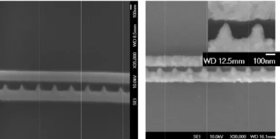
An SEM image of our fabricated geometrically-asymmetric device that we use in our own research is shown in Fig. 1. Note that we have chosen a device structure that has been fabricated on a large scale using standard nanofabrication techniques.
Ï
CMS
! 7®
Fig. 1. Lef distance~170 wall distance closed the gap the tips showT enormou physics, photovol of solar e sensing, applicatio of transm of the fre frequency P importan optimize ft: SEM image f 0nm. Right: SEM e~108nm. Energy-p. Also, no growt wing the selective n
The extensio us potential optical rec ltaics (the co energy to el and imaging on is the tran mitted inform equency. Fu y increases.1 erhaps in d nt challenges d so that: • The a visible • The re be rec sectio how t to fit capac result junctio areas u limitin kinetic
for the triangular M image at an interm
-dispersive X-ray th was observed on nature of the ALD
n of rectenn benefits. In tennas wou onversion of lectrical, the g (including nsmission an mation is gre urthermore, f 1,2 direct propo s in materials antenna is an e portion of ectifier has ctified. For n 2, we disc he geometri this require itance and c of recent ad on gaps can using selecti ng at gap se cs of the spe r antenna before rmediate stage of th spectroscopy (ED n the contact pad ( deposition. nas from th n addition t uld be usefu f photon ene ermal or che medical and nd reception ater at highe for transmis rtion to the s processing n efficient a the solar spe a response t
the solar sp cuss the con cally asymm ement. Th correspondin dvances in n now be rep ive ALD. In eparations of ecific materia
ALD. The Tip-w he ALD depositio DX) data after Cu A
(Al) and surroundi
he microwav to the break ul in many ergy to electr mical energ d chemical s n of informat er frequencie sion through e potential b g and theoret absorber of ectrum, curr time comme pectrum, λ ra ncept of trav metric tunnel is is demon ng RC time nanotechnolo producibly fa n particular, f f 1 nm. This als used in th
-wall gap distanc on. Tip-wall gap d ALD show that th ing SiO2 areas, as
ve to the IR kthroughs in y transforma trical energy gy), nano-ph sensors). An tion. This is es, where the h the atmosp benefits, op tical understa
radiation en rently not exp ensurate with anges from versal time a l junction (G nstrated by for a mode ogy, Metal/V abricated do for Cu, the s s is a conse he junction. F
ce~70nm; Tip len distance ~21nm; T he Cu successfully s expected. The in R and visibl n our unders ative applica y), solar cells otonics, nea nother increa s significant e density va phere, losse ptical rectific anding. The ncompassing ploited fully h the range 10,000 to ab and the RC t GATJ) desig a model ca el GATJ. M Vacuum/Meta own to ~1 nm selective AL equence of th
For gap dista
ngth ~100nm; W Tip length ~86.5nm y grew on the Pd nset is a magnified le regimes o standing of ations, inclu s (the conve ar field optic asingly impo since the de aries as the sq s decrease a cation has e device has g the energy y. of frequenci bout 400 nm time, and di gn can be tai alculation o Moreover, a al (MVM) tu m over cm2 LD process is he chemistry ances of this Wall-wall m; Wall-tips and view of offers basic uding ersion cs, IR ortant ensity quare as the faced to be y rich ies to m. In iscuss ilored of the as the unnel sized s self-y and s size,
rectification of radiation with frequencies in the visible range is possible due to the short transit time allowing electron tunneling before field reversal.
• Impedances must be matched for efficient energy collection and conversion in rectenna devices.
• The device has a high conversion efficiency. For a simple p-n junction PV cell, the efficiency is limited by the Shockley-Quissier Limit of about 33%.3,4 The theoretical understanding of the operation and description of antennas at the nanoscale in the optical regime is only now being studied in a rigorous way taking into account that the behavior of metals in the optical regime differs from that at frequencies below the IR.
In this paper, we discuss the modeling, characterization, and nanofabrication of a geometrically-asymmetric rectenna device that acts as both an antenna and rectifier for IR and optical radiation. In Section 2, we review the response time of such devices, focusing on the results and implications of an important study by Nguyen et al. We also explain how tunnel junctions are capable of rectifying signals in the visible regime. In Section 3, we review the mechanisms of rectification and the experimental data confirming optical rectification, including quantum-based theoretical analyses. We also show the significance of geometry in providing both the focusing effect and the asymmetric tunneling for rectification.
2. RESPONSE TIME OF TUNNEL JUNCTIONS
In addition to the issues regarding the fabrication of reproducible nanoscale devices, the response time of the rectifying device to optical radiation is a critical element for successful operation. The response time consists of several contributions. One is the collective response of the conduction electrons that establish the AC bias. Generally for metals, the collective response corresponds to frequencies well beyond the UV (or periods of about 10-16 sec). Two other elements affecting device response time are the electrodynamic response of the junction to the changing fields (RC-time) and the “transversal time” for electrons to cross the gap region in the tunnel junction before field reversal. These latter two times are considered in the following subsections.
2.A. “Traversal Time” or “Tunneling Time” for Nanoscale Tunneling Junctions
The concept of “traversal time” applied to electron transmission through time-dependent barriers, is needed to estimate the limiting frequency for the tunneling rectifiers used in nanoscale devices. Qualitatively, an electron of a given energy incident on the oscillating barrier “interacts” with the barrier for a time, τb. Consider the two limiting cases. In one limit where the period of the oscillation, T, of the radiation is longer than this time of interaction, the electron effectively interacts with a “static” barrier and, hence, can tunnel before the field direction reverses. On the other hand for the limit where the frequency of the radiation is very high with
T
b <<
τ , then the electron interacts with many cycles of the radiation and the tunneling barrier is essentially unchanged due to the oscillating voltage. In this limit, the tunneling current is comprised of the photon-excited electrons which have absorbed or emitted quanta equal to nhω, where n=1, 2,... and ω is the angular frequency of the incident radiation. The crossover between these two limiting behaviors may be determined by the relationship, ωτ ≈1.5 The validity of such a conceptual approach has been the subject of debate and controversy ever since
the advent of quantum mechanics and the recognition that there can be particle tunneling through classically forbidden barrier regions. Basically the problem lies in the difficulty of defining and measuring the traversal time for the simple time-dependent scattering experiment in which an electron represented by a wave packet tunnels through a spatially localized barrier and is detected beyond the tunneling region.6,7,8
A seminal experiment by Nguyen et al.9 used a dynamical approach to probe tunneling times in which a natural time scale is provided by a laser that is an integral part of the experimental arrangement. The laser incident upon an STM junction, consisting of a W-sharp tip and a polished, flat Si anode, causes the tunneling and, at the same time, provides a “clock” to measure the duration of the event. Given that the laser induced electric field is larger near the pointed apex of the tip than at the planar surface of the sample means that the vacuum tunnel barrier will tend to buckle inward (concave) or become thinner for forward bias and balloon outward (convex) or become thicker for reverse bias (see discussion and Figure 5 in Section 3.A). Moreover, if there is material asymmetry as in the Nguyen STM junction, there is an additional barrier asymmetry introduced. Such an STM junction can be a rectifier and under irradiation leads to a net DC current.
It can be argued that, if for a fixed spacing the laser frequency is too high, few electrons will be able to transfer from one electrode to the other during the half of the period when the electric field vector in the laser beam accelerates the tunneling electron. This means that one should observe a cutoff in the strength of the rectified DC signal either 1) when the frequency is increased beyond a critical value while maintaining the tip-to-surface distance s fixed or 2) when the gap width s is increased beyond a characteristic value s , while keeping the laser frequency e
constant. This latter method was used in these experiments by Nguyen, when the junction was illuminated by a 1.06-μm YAG laser. The tip-to-base gap s was then progressively increased until the laser-induced current vanished. The DC rectified current as a function of gap width for fixed frequency indicated a cutoff distance of about 2.5 nm for the 1.06 mμ YAG laser line.
The Nguyen study explained such experimental results in terms of a simple model that assumes that the particle acts as if it obeys the kinematical equations of motion as the particle traverses the classically inaccessible region defining the barrier at a velocity approximately equal to the Fermi velocity. If we assume an average tunneling velocity to be the Fermi velocity, v , F
then fcutoff =vF /s. This analysis predicts that for a 1 nm gap with a metallic tip and vacuum barrier, the transit time of about 10-15 seconds corresponds to radiation approaching the UV.9 The technological difficulty of producing arrays of nanometer gap junctions over areas of cm2 has recently been overcome by Gupta and Willis using selective ALD.10 Planar arrays of Cu-vacuum-Cu tunnel junctions were produced on silicon wafers using conventional lithography techniques, followed by selective ALD to yield tunnel junctions of ~ 1nm. This selective atomic layer deposition (ALD) process that is self-limiting at gap separations of 1 nm for Cu. At this spacing, the tunneling time is sufficiently short for electrons to transit the barrier before field reversal in the visible frequency range, leading to rectification for asymmetric barriers.
These estimates for the “traversal” time have been corroborated in a series of simulations by Mayer et al.11,12,13,14,15, who have used a quantum-mechanical transfer matrix approach for the modeling of a geometrically-asymmetric, metal-vacuum-metal junction subject to an oscillating potential. This quantum mechanical scheme accounts for the three-dimensional aspects of the
problem as well as the time dependence of the barrier. The currents are obtained by solving the time-dependent Schrödinger equation with a Floquet expansion of the wave function. For simulations using a full range of frequencies in the solar spectrum, Mayer et al. investigated how the efficiency of the rectification is affected by the aspect ratio of the tip, the work function of the metallic elements and the occurrence of polarization resonances. Their results demonstrate that the rectification of infrared and optical radiation is possible using devices of the type proposed by the authors.
2.B. RC-Time for Geometrically-Asymmetric Tunneling Junction (GATJ) Rectifiers For the case of a planar MIM structure, the RC response-time of the junction is limited by parasitic capacitance yielding a practical limit of 10-100 THz.16 By contrast, point-contact devices (i.e., whisker diodes, and GATJs whose geometry is essentially the same) have been used in measurements of absolute frequencies up to the green part of the visible spectrum, demonstrating a response time of the order of femtoseconds, orders of magnitude faster than conventional MIM diodes.17 The asymmetrical, non-planar geometry of the pointed whisker in conjunction with the flat anode is an essential requirement for increasing the cutoff frequency ωc of the diode, but inconsistent with the planar geometry of MIM tunneling theory for which the cutoff frequency is independent of contact area. In earlier studies of the detection and harmonic generation in the submillimeter wavelength region, Dees18 emphasized the importance of using the point-contact geometry to reduce the shunting effect of the capacitance and thus increase the high frequency cutoff of the device. Indeed the response time τ =1/ωc =RC is independent of contact area for a planar MIM geometry since C, the capacitance of the contact, is proportional to A, the contact area, whereas R the resistance is inversely proportional to A. On the other hand, for a point contact geometry, it can be shown using a solvable model with a spherical tip that ωc is no longer independent of the tip radius (or area), and the sharper the tip, the faster the response time of the diode.16,19 Although mechanical stability of these earlier devices placed a limitation on producing robust sharp tips, modern fabrication techniques have overcome the mechanical fragility of previous point contact diodes and issues related to reproducible fabrication of nanoscale devices.
Below we provide a more detailed discussion of why it is necessary to use GATJs with sharp tips to obtain RC times short enough for rectifying radiation at high frequencies.
Such models are important for understanding individual device operation and final integration of devices into complex circuits. These device-circuit equivalents, such as that for a tunneling diode, allow for the direct application of the Kirchhoff Current and Voltage Laws which are, in turn, applications of conservation of charge and energy. In determining the equivalent device model, resistances (R), capacitances (C) and inductances (L) are used either as lumped ( wavelength independent) or distributed (wavelength dependent, transmission line, R,L,C per unit length) elements.
For the case of the rectenna with a GATJ rectifier, a lumped circuit model consists of a resistance for the metallic antenna taking into account its geometric properties (i.e., the tip that is part of the GATJ) while the junction is modeled as a capacitance with a large shunt resistance. This junction corresponds to the traditional modeling of a low leakage capacitor. Such a junction and resistive line feeding element represent a single time constant circuit as illustrated in Fig. 3. It can be shown that this transient circuit has a time constant τ given by:
e Switch
wr-.
t
⎜⎜ ⎝ ⎛ = RC τ Fig. 3. Equ with junctio The lump elements (not vacu modeled curvature radius, th A an ac sign as the fre half-max 1 R ω = + For 2C c ω 2 2 cC R Rs ω We now proportio = C R ω ⎟⎟ ⎠ ⎞ + s S R R R uivalent circuit on shunt resista ped circuit e . It should b uum), the qu as a spheric e of the tip. H he shorter the Alternatively nal rather tha equency at w ximum power 2 2 2 s c s R C R ω . 1 2 2R >> , th 1 R= demonstrate onal to A, and 2 ( 1 ∝ sRC R model of a rec ance Rs element R in be noted that uantities R−1 al tip, the an Hence, the re e response tim we can con an under tran which half the r limit for op his leads to th e that ωc is d Ris inverse 1 2) ( / 1 1 − s s r r r π π ctenna with me n Fig. 3 incl except for t , C, and 1 s R− ntenna resista esponse time me.nsider the sam nsient condit e power is di peration, the he following proportional ely proportio 2 / 1 2 2) − ∝ s s r r tallic antenna r ludes implic the pointed a 1 are all prop ance R is pro e RC is propo me circuit bu tions.19 Follo issipated in th result is: condition fo l to 1/2 s r− . T onal to r ; hes resistance R an
citly the geom antenna tip c portional to oportional to ortional to rs ut analyze it owing Sulliv the series res
or ωc, The quantity ence, nd junction capa metrical nat coupled to th A. Howeve o 1 s r− , the inv s r or A . T1/2 ts steady-stat van et al.19, w sistance R. F C is propor (1) acitance C in p ture of the c he junction a er, for an an verse of radi The smaller th te behavior u we now defin For this tradit
(2) (3) rtional to A, (4) parallel circuit anode ntenna ius of he tip under ne ωc tional s R is
As the tip radius decreases the cutoff frequency increases. This reasoning led to the use of “ultra-fine” tips in the absolute frequency measurements of Javan and collaborators20 in which a thin, Tungsten wire several microns in diameter and approximate length of 1 mm was mounted at the end of a coaxial cable. The tip of the W wire was sharpened by means of a standard etching technique to a diameter of less than 100 nm.
Although neither the transient nor ac circuit approaches truly represent the GATJ but represent reasonable models for the rectifier, these approaches indicate that the RC response of the GATJ depends on the radius of curvature of the tip or contact area. The RC time constant has a dependence ranging between being proportional to r and s 1/2
s
r , thus predicting that sharp tips used
in the GATJ rectifer can be used to produce devices that can rectify radiation in the visible region. As an example, we estimate the RC time constant of a rectenna with a GATJ (coupled to
the anode) device with geometric parameters associated with one of our prototype devices similar to the one illustrated in Fig. 1. We consider a typical periodic unit cell of this device, with a single nanoantenna. The prototype device consists of ten thousand unit cells, placed in parallel. For this first-order estimation of the RC time constant, we use material parameters that correspond to the limit when ω→0. It is understood that frequency-dependent parameters should be used when considering frequencies in the visible, in particular for frequencies at which polarization resonances occur. The experimental device is essentially a two-dimensional flat structure. The periodic unit cell in our modeling has a length Lx =350nm along the x-axis and a cathode-anode
spacing Ly=295nm along y. A value of 100 nm is taken for the thickness W of the structure. We represent the antenna by a flat triangle whose apex is replaced by a half-circular disc of radius rapex that connects smoothly to the sides of the triangle. Initially, before the ALD metallization, the antenna has a base B=110nm, a height H =245nm and a radius of curvature rapex =16nm. The gap spacing between the apex of the antenna and the anode is 50 nm. The Ohmic resistance is estimated from a simple model in which we represent the antenna by the succession of slabs. For Cu, we obtain an Ohmic resistance R=0.737Ω.
In order to determine the geometric capacitance C of a unit cell of the device, we calculate numerically the electrostatic energy CV2/ 2, under a static voltage
ac
V between the
cathode and the anode. The electric potential in the unit cell of the device is obtained by solving Laplace’s equation ∇(e∇V))=0 (this expression is relevant to the static limit in which ω→0
and the antenna is assumed to have a dielectric constant ε → −∞ ). The resolution of Laplace’s equation is achieved by using a finite-difference technique.21 This resolution provides the electric potential V r( ) in the system from which we can compute the electric field, E=−∇V . The geometrical capacitance C of the system considered is finally obtained from the relation
2 2
1 1
2CV =
∫∫∫
unit cell_ 2ε E dv (5)in which the right-hand side provides the electrostatic energy one must provide to a unit cell of the device in order to establish V . For the system represented in Fig. 14, we obtain a geometric ac
capacitance C=2.94 10× −18F and a resulting RC time constant of 2.2 10× −18 s, a value corresponding to frequencies beyond the visible.
d o U m O L)15) I ' ' ' I I(") 30 ip spacing (nrr W dimensio paramete ranges fr from 245 reduced p 110 nm t resistanc from 2.9 constant capacitan FIG. 4. Ca with the d between th increases f 0.737Ω. F not be a static val account t 3. RECT 3.A. M The I-V c initial sta temperatu shape of photovol We can study onal expansi ers B, H and rom 1 to 1.2 5 nm to 294 n progressivel to 132.45 nm e R of the an 18 94 10× − F increases f nce C as H in apacitance C o dilation parame he apex of the from 16 nm to
rom the sim limiting fact lues of the the frequenc TIFICATIO Mechanisms characteristi ates incident
ure and field f the tunne ltage effects y how the p ion of the apex r used fo 204. In this e nm, so that t ly from 50 n m. The param ntenna rema (for H =2 from 2.2 1× ncreases from of a unit cell o eter goes from antenna and th 19.3 nm. The
mulations, the tor for applic parameters y dependenc N IN TUNN for Rectific ics of a tunne t on the bar d, 2) the ava el barrier, w , induced A parameters R antenna. A or Fig. 3 are expansion, t the gap spac nm to 1 nm. meters L , Lx ins approxim 245 nm) to 18 0− s to 1. m 245 nm to of the device, w m 1 to 1.204. T he anode, as H Ohmic resistan e RC time c cations relat are applicab ce of the mat NEL JUNCT cation in Tu eling junctio rrier interfac ailable final which may AC voltages R, C and τ = A series of e multiplied b the height H cing between The base B y L and W of mately const 17 1.69 10× − F 17 .2 10× − s, o 294 nm is r
when the anten The results are H increases from
nce R of the an
constant of t ted to the rec ble. The ext
terial param TIONS unnel Juncti on are determ ce and their states and t be modifi due to lase RC = are m antennas ar by a commo H of the ante n the apex of of then incr f the device a tant. The geo
F (for H = respectively represented nna is affected e represented a m 245 nm to 2 ntennas includi the device st ctification o tension of th meters is curre ions mined by 1) occupation their occupa ied due to er irradiation modified by a re generated on dilatation ennas increa f the antenna reases at the are kept con ometric capa 294 nm = ) a y. This de in Fig. 4. d by a conform as a function o 294 nm and the ing the sharp t
tructures in f optical rad hese simula ently under the flux of e probabilitie ation probabi contact po n, etc. Corr a conformal d for which factor α wh ses progress a and the ano e same time stant. The O acitance C ra and the RC ependence o
mal planar exp of the gap spa e radius of cur ip is calculated this work sh diation, wher ations taking investigation electrons in g es that depen ilities, and 3 otentials, su respondingly two-h ttwo-he here α sively ode is from Ohmic anges time of the ansion cing d rvature d to be hould re the g into n. given nd on 3) the urface y, the
-we^ FORWARI ) -e % v14.. +V -v I current a several p photo-sti asymmet critical el 3.A. Rec For nano passes pr condition assuming function comprisin Fig. 5. (c) concave sh It than at th buckle in reverse b by Feens al.9 In a tunneling experime frequenc nonlinear to optica laser sou rectificat junctions the deve conversio asymmetry ( possible caus imulated cha try of the re lement for a ctification du ometer gap d redominantly ns and even g no work fu of the appl ng the tunne ) A tunnel bar hape for (a) for
t is evident t he planar su nward or be bias. The firs stra et al.25 a addition, Dag g diode can ents, they e ies. Most re r tunneling c al rectificatio urce. In a rec tion mechan s verify thes elopment an on of infrar or rectificati ses discussed anges in the ctenna due t chieving hig ue to Barrie distances, th y through th n in the abse unction inho lied bias fie el junctions.
rrier of a mater rward bias and
that the stati urface of the ecome thinne st observatio and in the de genais et al. n be used t envision that ecently, War conduction b on, producin cent paper, t nism.28 Exte e observatio nd optimizat red and opti
ion properti d below, nam electron flux to the modif gh frequency er Modifica he nature of hat sharp pro ence of any omogeneities eld. This is This effect i rially-symmetr (b) convex sha c electric fie sample. Th er for forwa on of the ge etailed study 26 have expe to rectify ra t higher co rd et al.27 ha between gol ng a DC ph the authors h ensive simul ons. In partic tion of dev ical radiatio es) at fixed mely materi x distribution fication of th y rectification tion by Asy f the tunnelin otrusion clos y material a s), the shape due to the is illustrated ric, geometrica ape for reverse
eld gradient is means tha ard bias and ometrical as y of rectifica erimentally v adiation thr onversion ef ave shown b ld electrodes otocurrent w have reviewe lations studi cular, the wo vices that c ons. The stu
gap width s ial, geometri n.22,23,24 We he field dist n. ymmetric G ng phenome sest to the pl asymmetry ( e of the tunn geometric a d in Fig. 5. ally-asymmetri e bias.9 is larger nea at the vacuu d balloon ou symmetry ef ation in an S verified that rough the R fficiencies w oth experim s separated b when the ga ed experime ies of geom ork of Maye could be us udies also d s must origi ical, thermal e describe he tribution in d eometry enon is such lanar sample (e.g., W tip, nel barrier is asymmetry o ic junction. T ar the pointe um tunnel ba utward or be ffect in a ST STM present t a geometri RF region. will be achi mentally and by a subnan ap is irradiat ents verifying metrically as er et al. prov ed for the demonstrate nate from o l asymmetry ere the geom device that i h that the cu e surface. In , W surface s asymmetric of the electr
The barrier exh
ed apex of th arrier will te ecome thicke TM was obse ted by Nguy cally asymm Based on ieved at mi theoretically ometer gap ted by a 78 g the geome symmetric tu vides insigh efficient en that an acc ne or y, and metric is the urrent n such , and c as a rodes hibits a he tip end to er for erved yen et metric their id IR y that leads 5 nm etrical unnel t into nergy curate
treatment of nanoscale tunnel junctions operating in the near IR and visible requires a quantum-mechanical treatment.11-15
3.B. Experiments Verifying Rectification Mechanisms from the Microwave through the Visible Region—Geometrical Effects
In this section we review some of the experiments verifying that an STM and other nano-junctions structures can act as antennas and rectifying devices for electromagnetic radiation from the microwave through the visible.
In a series of experiments, Kuk et al.29,30 used an STM consisting of a metal tip (Au) and a semiconductor sample anode (e.g., Si), which was illuminated with laser radiation below and above the semiconductor indirect band gaps, specifically, photon energies of 2.94 eV, 1.96 eV, 1.17 eV, and 0.95 eV. The STMs were modified using a small lens to focus the laser beam to near its diffraction limit, yielding power densities up to 5.0kW cm on the junction./ 2 31 The resulting induced bias was measured laterally along the surface as light-induced excess current and voltage. For photon energies exceeding the band gap energy, surface photovoltages (SPV) of about 300 mV were induced across the gap independent of illumination intensity and frequency. For a photon energy of 0.95 eV, no surface photovoltage was detected. A small, atomically scaled (laterally along the surface) varying dc signal of 3 to 5 mV was also observed in the experiments. The authors suggest that this small signal is due to optical rectification associated with the geometric asymmetry of the junction. These striking results using a Au tip and collector demonstrate that the STM junction can absorb and rectify radiation corresponding to wavelengths shorter than 1.06 µm in agreement with the experimental results of Nguyen et al.9
Tu et al.32 have experimentally verified that an STM junction can rectify radiation in the microwave region, which has led to the first direct, quantitative measurement of the rectification current due to single atoms and molecules. In their work, microwave of known amplitude and frequency irradiated the junction of a low temperature scanning tunneling microscope producing an electric field between the tip and an atom or molecule on the anode surface. It induced a DC signal that is spatially localized and exhibits chemical sensitivity at the atomic scale.
In 1998, Bragas et al.,33 used a laser with wavelength of 670 nm to irradiate an STM junction to determine the field enhancement as measured by optical rectification. A field enhancement factor between 1000 and 2000 was obtained for highly oriented pyrolytic graphite and between 300 and 600 for gold. Analysis of their data indicated optical rectification due to junction geometry as well as thermal asymmetry. The admixture of 2 / 2
dc
stat stat V
I V
∂ ∂ was
determined to be significant only for p-polarized light and in phase with the intensity variation, consistent with the expected behavior for the rectified current. Their experiments indicate that visible light (640 nm) can be rectified using nm-sized tunnel junction devices.
Most recently, Ward et al. have shown both experimentally and theoretically that “nonlinear tunneling conduction” between gold electrodes separated by a subnanometer gap leads to optical rectification when the gap is irradiated by a 785 nm laser source, producing a DC current.27
1 1 1 "' 0.7 0.8 0.9 1 1 0.1 0.2 0.3 "'1 1 1 "' 0.4 0.5 0.6
Applied bias (Volt)
U nanowire illustrate compared (with r→ reverse c Fig. 6. Ef junction; (b E approxim typically make it p including Such stud that are im L dimensio theory. T parallel e of each distributi on transf STM mic A point sou single ato agreemen filtering the partic Unlike a con e tip achieve d in Fig. 6 w d using plan → ∞) provid current) of on
ffect of tip rad b) r=10nm; Early theoreti mations in t based on a possible to a g three-dime dies make it mportant in Lucas et al.3 onal, non-sep They applied electrodes, o metal elect ion peaks wi fer-Hamilton croscope, wh A theoretical urce of elec om yield a r nt with expe by an adiab cular geomet nventional p e rectificatio where the re nar and poin des no recti ne.34 ius, r, on the r (c) r=2nm; ical work on the shape o a one-dimen address this ensional asp t possible to optimizing t 37 used a f parable, spat d this approa one of which trode is ass ithin a narro nian formalis hen operatin l study by N ctrons indica relatively fo erimental stu atic constric try, planar MIM on solely or ectification r nted geometr fication, i.e rectification ra ; (d) r=1nm; n the tunnelin of the barrie nsional mod problem mo pects of the o investigate the performa formulation tially-localiz ach to a mo h containing sumed to be w angle arou sm and in a ng with atom N. D. Lang,
ates that the ocused, high udies.38 The r ction. This i M or MVM primarily w ratio of a W ries. Figure ., a rectifica
atio. The calcu ; and (e) r=0. ng character er and in th del.6,36 Ho ore rigorousl detailed ato the geometr ance of geom of elastic, zed barriers w del metal-va a hemisphe e free-electr und the boss greement w mic-size tips. A. Yacoby e current fro -current bea results are p is a consequ M diodes, de with geometr W-W junction e 6 shows cl ation ratio ( ulations were d .5 nm, all for a ristics of the he tunneling owever, mod ly using qua omic structur ric, material metrically-as one-electro within the c acuum-meta erical protrus ron-like. T s axis, confir with the obse
and Y. Imr om a field-e am with a na physically in uence of the evices empl rical asymm n (no materi learly that a (forward cu
done for (a) r a separation of se junctions g probabilit dern comput antum-mecha re and the t l, and operat symmetric d on tunneling context of po al junction, c sion. The ele They found rming earlie erved atomic ry in 1989 o emission tip arrow energ nterpreted in e potential di loying a po metry.34,35 Th ial asymmetr planar geom urrent divide → ∞, planar-f 2 nm.34 usually relie ties, which tational faci anical techn tunneling ba tional param evices. g through t otential-scatt consisting o ectronic stru that the cu er estimates b c resolution on a single-terminated gy distributio terms of ch istribution d ointed his is ry) is metry ed by -planar ed on were ilities niques arrier. meters three-tering f two ucture urrent based of an -atom by a on, in annel due to 3.C. Simulation Studies of Geometrically Asymmetric Tunnel Junctions
Mayer et al.11 presented a transfer-matrix analysis of a GATJ with a flat anode and a cathode with a hemispherical protrusion. This work confirmed the conclusions of Lucas et al.34 and explored how the rectification properties of such systems depend on their physical and geometrical parameters. This analysis still relied on a quasi-static approximation, in which it is assumed that one can compare currents obtained for static values of the external bias. This approximation is valid in the far-infrared (ω→0) but must be replaced by a more exact approach in order to treat situations in which the time that electrons take to cross the junction is comparable with the period of the oscillating barrier.
In a subsequent paper Mayer et al.12 extended their previous work by taking into account the time dependence of the external bias explicitly using the transfer-matrix approach and the time dependent Schrödinger Equation. They assume that the geometrically asymmetric tunnel junction consisted of a cathode metal supporting a hemispherical protrusion with a height of 1 nm, a radius of 0.5 nm, and separation between the apex of the tip and the planar electrode of 1 nm. Due to the external electromagnetic radiation of varying frequency and intensity, there is an impressed oscillating potential across the junction, V t
( )
=Vaccos( )
ωt . In the simulations, V acvaries from 0.01V to 1.0V and frequencies that correspond to quanta of energy between 0.2 eV (
6200 nm
λ = ) in the IR and 5eV (λ=248nm) in the UV. The rectification ratio that one obtains by taking the ratio of the mean values of the forward, I+, and reverse, I−, currents is plotted in Fig. 7. The values obtained at low frequency, ω→0, agree with those obtained in the quasi-static analysis.11 Because of the photon-absorption processes, the rectification ratio, R, first increases with ω before decreasing at higher frequencies. The intermediate region proves that the rectification of optical frequencies can be achieved by the device, which agrees with conclusions reached earlier by Sullivan, et al.16 In a quasi-static analysis, they predict a cutoff of the rectification for a photon-energy around 4 eV (radiation with wavelength of 300 nm in ultraviolet) because the field would then reverse before the electrons can cross the junction. Indeed, this oscillating-barrier analysis shows a significant decrease in rectification at that frequency.
1r TI r I I I I I I I I I I I I I I I I Fig. 7. R
(
cos ac V ωt ranges betw Fermi leve In plasmoni junction, irradiated and curre energetic plasmons rectificat Compare rectificat correspon T material is the mo is a signi pronounc devices f efficient ectification ra)
t with Vac = ween 0.2 and el of the emittin n order to a ic resonance Mayer et a d MVM tunn ent output du c green port s and more tion properti ed to tungst tion ratio of nd to a reson These results and the geom ost efficientificant contri ced when a for the selec rectification atio as obtaine 1 (solid line), 5 eV. The ve ng metal) when assess the im es, on the fie
al. performe nel junctions ue to the sur tion of the v generally o ies of the j ten, the po the device a nant polariza s suggest th metry of the for the rectif ibution of m polarization ctive detectio n and conver ed for a geom 0.1 (dashed_) rtical lines ind n V (dashed lac mportance o ld enhancem ed 3D quan s using Ag a rface plasmo visible spec of the frequ junction. In wer gained are enhanced ation of the t hat the dep e tip could be fication of e multi-photon n resonance on of radiat rsion of their metrically asy ) and 0.01 V dicate the heig
line, left), −1 (
of the depo ment and rect ntum mechan and W tips.1 onic resonan trum. This uency-depend n Fig. 8, we by the ele d by several tip. endence of e used to con external sign processes (e occurs. Th tion in the in r energy. It i ymmetric junc (dot-dashed li ght of the surfa (dashed line, rig
osition of no tification pro nical compu 3 They pred nces in Ag at s study also dence of th e plot the r ectrons that l orders of m f the plasmo ntrol the fre nals. It is also especially fo his effect op nfrared or v is expected t ction subject ine). The quan face barrier (as ght), and 0 V ( oble metals, operties of a uter simulat dict an enhan t ~3 eV, corr explained t he dielectric results of th t cross the magnitude at on frequenc quency at w o important orhω ≈ eVac pens the po visible doma that depositi to an externa ntum of energ s measured fro (solid Line).12 , known to a model tunn tions of opti nced rectific responding t the role of function on heir simulat device, and t frequencies cies on both which the jun
to note that c ), which is ossibility to ain or for a on of a thin al bias gy h ω om the have neling ically cation to the these n the tions. d the s that h the nction there most build more layer
ext
1 ¡
/'-Vext)
Quantum 2 of energy of other aluminum Fig. 8. Re and 0.01 V( )
1 ε ω = − 3.1 eV reso M frequenc resonanc possibilit of extern increases in which The curr for a sing radiation geometri quantitat converted T devices t The stud in the nea noble meta m should yie ctification ratio V. The solid, da(
2 2 / p i ω ω ω − + onance energy Mayer et al. ies that cor e frequencie ty of control nal radiation. s the performdevices wou ents and ene gle tip times n with typica cally asymm ive analysis d by such de The work of that could be dies also dem ar IR and vis
als on an un eld similar re
o of a junction ashed and dot–
)
/ ω τ , respect with ε ω( )
= . also obser respond to es on the sh lling the freq . It also was mance. For p uld be place ergies achie s a typical fa al frequencie metric, meta s of the eff evices. f Mayer et a e used for th monstrate tha sible require nderlying an esults. made of silver dashed lines in tively, as mode 2 2 1−ω ωp/ are rved a sign a resonant hape and on quency at w s shown that practical app d with a typ ved per squ actor of 1010 es in the infr al–vacuum– ficiency wit al. provides he efficient e at an accura es a quantum ntenna struc r and subject to ndicate results u els for the diele e off-scale andnificant enha polarization n the mater which the dev
t reducing th plications, o ical spacing uare meter co . These res rared and op –metal junct th which th insight into energy conv te treatment m-mechanica cture such a o an external b using ε ω
( )
→ ectric function not shown.13 ancement o n of the tip. rial used for vice is most he work func one may con g of 10 mμ b orrespond in sults demons ptical domai tions. The r he energy o o the devel version of in t of nanosca al treatment.1 as tungsten, bias Vaccos(
ωt → −∞ , ε ω( )
= of the tip. Resof the energ 14 The depe r the tip the efficient for ction of the m sider two-di between adja n this case t strate that th ins can be a results also of incident r opment and frared and o ale tunnel jun
11-15 molybdenu
)
, with Vac =1 2 2 1 ω ωp/ = − , a sults obtained gy conversio endence of erefore give r the rectific metallic elem imensional a acent protrus to those ach he rectificati chieved by u provide a radiation ca d optimizatio optical radiat nctions oper um or 1 , 0.1 and at the on at these es the cation ments arrays sions. ieved on of using more an be on of tions. rating5. SUMMARY
We have surveyed developments related to the fabrication and theoretical understanding of our proposed nanoscale rectennas. These rectenna devices, based on the geometrically-asymmetric tunnel junction, can collect and rectify electromagnetic radiation, from the infrared through the visible regimes. Studies of electron transversal time and RC response time demonstrate that tunnel junctions formed with a sharp tip (early examples of which are the whisker diode and the STM probe) are capable of operating into the UV regime. Recent efforts to construct nanoscale antennas reveal a wealth of promising geometries and fabrication techniques. Other recent experimental work confirms that nanorectennas are capable of not just receiving, but also rectifying, signals through the visible regime. A number of past and recent ongoing simulation studies not only demonstrate the viability of the geometrically-asymmetric tunnel junction, but also establish the importance of certain design parameters (choice of geometry and materials) that will be crucial in efforts to optimize such devices.
Acknowledgements
We thank Dr. Moon S. Chung (Ulsan University, Ulsan, S. Korea) and Dr. A. A. Lucas (Universitaires Notre-Dame de la Paix, Namur, Belgium) for their useful reviews and critiques. We also acknowledge the assistance of and useful discussions with William Mansfield, former Director of Operations of the Nanofabrication Laboratory at The Pennsylvania State University, and his associates at the facility. This work was supported in part under NSF Grant No. 1231313, Division of Electrical, Communications and Cyber Systems, under the Program: Energy, Power, Adaptive Systems-EPAS.
1 J. Alda, J. Rico-García, J. López-Alonso,and G. Boreman, “Optical antennas for nano-photonic applications,”
Nanotech. 16, S230 (2005).
2 Palash Bharadwaj, Bradley Deutsch, and Lukas Novotny, “Optical Antennas,” Adv. Opt. and Photonics 1, 438
(2009).
3 P. B. Lerner , N. M. Miskovsky, P. H. Cutler, A. Mayer, and Moon S. Chung, “Thermodynamic Analysis of High
Frequency Rectifying Devices: Determination of the Efficiency and Other Performance Parameters,” Nano Energy, Volume 2, Issue 3, 368–376 (2013).
4 Saumil Joshi and Garret Moddel, “Efficiency limits of rectenna solar cells: Theory of broadband photon-assisted
tunneling,” Appl. Phys. Lett. 102, 083901 (2013).
5 M. Büttiker and R. Landauer, “Traversal Time for Tunneling,” Phys. Rev. Lett. 49, 1739 (1962). 6 C. B. Duke, Tunneling in Solids, New York, Academic, 1969.
7 P. H. Cutler, T.E. Feuchtwang, T. T. Tsong, Y. Kuk, H. Nguyen, and A. A. Lucas, “Proposed use of a
scanning-tunneling-microscope tunnel junction for the measurement of tunneling time,” Phys. Rev. B 35, 7774 (1987).
8 L. V. Keldysh, “Ionization in the Field of a Strong Electromagnetic Wave,” J. Exptl. Theoret. Phys. (USSR) 47
(1964) 1945-1957, translation: Soviet Physics JETP 20 (1965) 1307-1314. Keldysh presented another, not altogether incompatible, criterion for adiabatic transmission through the oscillating barrier. The crossover between the multiphoton absorption and the quasi-static tunneling is determined by the Keldysh parameter
(
2 2)
1/22 /
K m V e Ee b
γ =ω , where me is the electron mass, e the charge on the electron, E is the electric field strength
generated by the laser and ω is the angular frequency of the radiation. In the case of a metal, the height of the barrier, Vb, is typically identified with the work function and for a semiconductor with the band gap. As would be
expected a value of γK >> indicates multiphoton processes dominate (in the barrier and/or tunneling process), and, 1 1
K
γ << implies tunneling processes dominate.
9 H. Q. Nguyen, P. H. Cutler, T. E. Feuchtwang, Z–H. Huang, Y. Kuk, P. J. Silverman, A. A. Lucas, and T. E.
Sullivan, “Mechanisms of Current Rectification in an STM Tunnel Junction and the Measurement of an Operational Tunneling Time,” IEEE Trans. Elec. Dev. 36, 2671 (1989).
10 R. Gupta and B.G. Willis, “Nanometer spaced electrodes using selective area atomic layer deposition,” Appl.
Phys Lett. 90, 253102 (2007).
11 A. Mayer, M.S. Chung, B.L. Weiss, N.M. Miskovsky and P.H. Cutler, “Three-dimensional analysis of the
geometrical rectifying properties of metal-vacuum-metal junctions and extension for energy conversion,” Phys. Rev. B 77, 085411 (2008).
12 A. Mayer, M.S. Chung, B.L. Weiss, N.M. Miskovsky, P.H. Cutler, “Three-dimensional analysis of the rectifying
properties of geometrically asymmetric metal-vacuum-metal junctions treated as an oscillating barrier,” Phys. Rev. B 78, 205404 (2008).
13 A. Mayer and P.H. Cutler, “Rectification properties of geometrically asymmetric metal-vacuum-metal junctions: a
comparison between tungsten and silver tips to determine the effects of polarization resonances,” J. Phys. Condens. Mat. 21, 395304 (2009).
14 A. Mayer, M.S. Chung, B. L. Weiss, N. M. Miskovsky and P. H. Cutler, “Simulations of infrared and optical
rectification by geometrically asymmetric metal–vacuum–metal junctions for applications in energy conversion devices,” Nanotech. 21, 145204 (2010).
15 A. Mayer, M.S. Chung, P.B. Lerner, B.L. Weiss, N.M. Miskovsky and P.H. Cutler,” Classical and quantum
responsivities of geometrically asymmetric metal-vacuum-metal junctions used for the rectification of infrared and optical radiations,” J. Vac. Sci. Tech. B 29, 041802 (2011); A. Mayer, M.S. Chung, P.B. Lerner, B.L. Weiss, N.M. Miskovsky and P.H. Cutler, “An analysis of the efficiency with which geometrically asymmetric metal-vacuum-metal junctions can be used for the rectification of infrared and optical radiations,” J. Vac. Sci. Technol. B 30, 031802 (2012).
16 T. Sullivan, Young Kuk, and P. H. Cutler, “Proposed Planar Scanning Tunneling Microscope Diode: Application
17 K. M. Evenson, “Frequency measurements from the microwave to the visible, the speed of light, and the
redefinition of the meter,” in Quantum Metrology and Fundamental Physical Constants, P. H. Cutler and A. A. Lucas, Eds. New York: Plenum, 1983.
18 J. W. Dees, “Detection and Harmonic Generation in the Submillimeter Wavelength Region,” Microwave Journal
9, 48 (1966).
19 T. E. Sullivan, Ph. D. thesis (1977), “Thermal and field emission effects of laser radiation on metal whisker
diodes: Application to infrared detection devices,” available from UMI (University Microfilms International), now called Bell and Howell Information and Learning.
20 A. Sanchez, S.K. Singh, A. Javan, “Generation of infrared radiation in a metal-to-metal point-contact diode at
synthesized frequencies of incident fields: a high speed broad-band light modulator,” Appl. Phys. Lett. 21. 240 (1972).
21 A. Mayer and Ph. Lambin, “Calculation of the electrostatic forces that act on carbon nanotubes placed in the
vicinity of metallic protrusions,” Nanotech. 16, 2685 (2005).
22 N.M. Miskovsky, S. J. Shepherd, P. H. Cutler, T. E. Sullivan, and A. A. Lucas, “The importance of geometry,
field, and temperature in tunneling and rectification behavior of point contact junctions of identical metals,” Appl. Phys. Lett. 35, 560 (1979).
23 N. M. Miskovsky, P. H. Cutler, T. E. Feuchtwang, S. J. Shepherd, A. A. Lucas, and T. E. Sullivan, “Effect of
geometry and multiple-image interactions on tunneling and I-V characteristics of metal-vacuum-metal point contact junctions,” Appl. Phys. Lett. 37, 189 (1980).
24 Stefan Grafström, “Photoassisted scanning tunneling microscopy,” J. Appl. Phys. 91, 1717 (2002), and references
therein.
25 R. M. Feenstra. J. A. Stroscio, and A. P. Fein, "Tunneling spectroscopy of the Si( 111) 2 x I , surface," Surf. Sci.
181, 295 (1987).
26 M. Dagenais, K. Choi, F. Yesikoy, A. N. Chryssis, M. C. Peckerar, “Solar Spectrum Rectification Using
Nano-Antennas and Tunneling Diodes,” Proc. SPIE, Vol. 7605, 76050E-1 (2010).
27 Daniel R, Ward, Falco Hüser, Fabian Pauly, Juan Carlos Cuevas and Douglas Natelson, “Optical rectification and
field enhancement in a photonic nanogap,” Nat. Nanotechnol. Lett. 5, 732 (2010).
28 Nicholas M. Miskovsky, Paul H. Cutler, A. Mayer, Brock L. Weiss, Brian Willis, Thomas E. Sullivan, and Peter
B. Lerner, “Nanoscale Devices For Rectification Of High Frequency Radiation From The Infrared Through The Visible: A New Approach,” Journal of Nanotechnology (2012).
29 Y. Kuk, R. S. Becker, P. J. Silverman, and G. P. Kochanski, “Optical Interactions in the Junction of a Scanning
Tunneling Microscope,” Phy. Rev. Lett. 65, 456 (1990).
30 Y. Kuk, R. S. Becker, P. J. Silverman, and G. P. Kochanski, “Photovoltage on silicon surfaces measured by
scanning tunneling microscopy,” J. Vac. Sci. Technol. B 9, 545 (1991).
31 In comparison, an estimate of the power density for a laser with a power output of 20mW and a beam diameter of
about 300 µm is on the order of 20 W/cm2.
32 X. W. Tu, J. H. Lee, and W. Ho, “Atomic-scale rectification at microwave frequency,” J. Chem Phys. 124,
021105 (2006).
33 A. V. Bragas, S. M. Landi, and O. E. Martinez, “Laser field enhancement at the scanning tunneling microscope
junction measure by optical rectification,” Appl. Phys. Lett. 72, 2075 (1998).
34 A. A. Lucas, A. Moussiaux, M Schmeits, and P. H. Cutler, “Geometrical asymmetry effects on tunneling
properties of point contact junctions,” Commun. Phys. 2, 169 (1977).
35 Bo Lee, E. F. Barasch, T. Mazumdar, P. M. McIntyre, Y. Pang, H. J. Trost, “Development of knife-edge field
emission cathodes on (110) silicon wafers,” Appl. Surf. Sci. 67, 66 (1993).
36 P. H. Cutler, Jun He, J. Miller, N.M. Miskovsky, B. Weiss, and T.E. Sullivan, “Theory of Electron Emission in
High Fields from Atomically Sharp Emitters: Validity of the Fowler-Nordheim Equation,” Prog. In Surf. Sci. vol. 42, 169 (1993).
37 A. A. Lucas, H. Morawitz, and G. R. Henry, J.-P. Vigneron , Ph. Lambin, P. H. Cutler and T. E. Feuchtwang,
“Scattering-theoretic approach to elastic one-electron tunneling through localized barriers: Application to scanning tunneling microscopy,” Phys. Rev. B 37, 10708 (1988).