HAL Id: hal-00673568
https://hal-iogs.archives-ouvertes.fr/hal-00673568
Submitted on 24 Feb 2012
HAL is a multi-disciplinary open access
archive for the deposit and dissemination of
sci-entific research documents, whether they are
pub-lished or not. The documents may come from
teaching and research institutions in France or
abroad, or from public or private research centers.
L’archive ouverte pluridisciplinaire HAL, est
destinée au dépôt et à la diffusion de documents
scientifiques de niveau recherche, publiés ou non,
émanant des établissements d’enseignement et de
recherche français ou étrangers, des laboratoires
publics ou privés.
Photorefractive wave mixing in undoped LEC GaAs at
1.5µm : validation of photorefractive modeling
Philippe Delaye, Louis-Anne de Montmorillon, H.J. von Bardeleben, Gérald
Roosen
To cite this version:
Philippe Delaye, Louis-Anne de Montmorillon, H.J. von Bardeleben, Gérald Roosen. Photorefractive
wave mixing in undoped LEC GaAs at 1.5µm : validation of photorefractive modeling. Applied
Physics Letters, American Institute of Physics, 1994, 64 (20), pp.2640-2642. �10.1063/1.111477�.
�hal-00673568�
Photorefractive
wave mixing in undoped liquid encapsulated
Czochralski
GaAs at 1.5 pm: Validation
of photorefractive
modeling
P. Delaye and L. A. de Montmorillon
Institut d’optique Theorique et Appliquee, Unite de Recherche Associee 14 au Centre National de la Recherche Scientifique, Bat. 503-Centre Scientijque d’Orsay, B. l? 147-91403 Orsay Cedex, France
H. J. von Bardeleben
Groupe de Physique du Solide, Unite de Recherche Associee 17 au Centre National de la Recherche Scientijique, Universite Paris 6 et Paris 7, 2 Place de Jussieu, 75005 Paris, France
G. Roosen
Institut d’optique Theorique et Appliquee, Unite de Recherche Associee 14 au Centre National de la Recherche Scientifique, Bat. 503-Centre Scientijque d’Orsay, B.P. 147-91403 Orsay Cedex, France
(Received 4 January i994; accepted for publication 25 February 1994)
We present photorefractive measurements in undoped GaAs performed at 1.06 pm, 1.32 ,xm, and at
u”
1.55 ,um. Using concentrations of EL2 that we determined through optical absorption and
electron paramagnetic resonance measurements in the same sample, we show that a single defect model with an electron-hole competition quantitatively explains our results of photorefractive wave
The photorefractive effect (PRE) is based on the redis- tribution of charges in a deep defect under a nonuniform illumination. The effect is thus closely linked to the photo- ionization properties of this deep defect. Discussions cur- rently occur on the exact nature of the deep levels that are
source of the photorefractive effect in III-V and II-VI
materials.rm3 GaAs is the most studied among the infrared photorefractive materials, for ten years4 and correlations were found between the occupancy of the EL2 defect esti- mated from absorption measurements and the photorefrac- tive performances of samples issued from different parts of the same ingot.5 We present a comprehensive analysis of semi-insulating GaAs for the sensitivity range of this mate-
rial, i.e., l-l.55 r(Lm, with different techniques, such as op-
tical absorption, electron paramagnetic resonance (EPR), and photorefractive effect. On a given sample, we determine the EL2 total concentration as well as the EL2 defect occupancy and photorefractive energy transfer gain. Comparison of theoretical predictions and experimental data obtained for the
three wavelengths 1.06, 1.32, and 1.55 p are presented and
discussed, showing that the PRE is perfectly explained by the presence of the EL2 native defect.
The electrical compensation at T= 300 K of undoped semi-insulating GaAs grown by the liquid encapsulated Czo- chralski (LEC) technique from pyrolytic BN crucibles has been successfully described in a three defect model based on the interaction of shallow effective mass like donors No, shallow effective mass like acceptors NA, and the deep double donor EL2 with its O/+level at EC-O.748 eV! Typi- cal concentrations in state of the art materials are NDp1014
cmd3, N,%(2-5)X 1Or5 cmB3, and NEL2=2X 10¹⁶ cmM3.
The EL2 defect is responsible for the extrinsic photocon-
ductivity of this material in the l-l.5 ,Z wavelength range.
With the Fermi level pinned by the EL2”+ level we have the
possibility of the two transitions: EL2’-+EL2++e& and
EL2+-+EL2’+& with the corresponding photoionization
cross sections S, and S, , whose absolute values have been determined in the wavelength range of interest.7 From the
curve at 300 K in Ref.7 we deduce: S,,, = 1 X lo-t6 cm’ and
S,=4XlO-r7 cm2 at 1.06 ,um, and S,=1.5XlO-t7 cm2 and
Sp=5X10-17 cm* at 1.32 ,um. For h=1.55 p,
S,=2XlO-t7 cm2 and no value can be extracted on this
curve for S, . In order to determine the value of S, , we use the result at 78 K which gives a ratio S,/(S, f S,) that is
nearly the same at 1.32 and 1.55 w. Assuming that this
property is preserved at 300 K, we deduce S,=5X10-18 cm’.
The modeling of the energy transfer gain in photorefrac- tive two-beam coupling experiments requires the knowledge of the EL2’ and EL2+ concentrations. Both of them can be obtained by pure optical absorption measurements at the two different photon energies h vl and h v2 according to:
where LY and S are the absorption coefficient and the photo- ionization cross section, respectively.* However, it has been shown that this all-optical method is not sufficiently reliable for the determination of the EL2+ concentration.* Therefore we prefer to determine the EL2+ concentration from the in- tensity of the EL2+ related EPR spectrum. The optical ab- sorption coefficient c~ (Fig. 1) is determined from a trans-
mission experiment and deduced with the formula:
T=(l -R)2exp(-ru2)/[l-R2exp(-2cul)] for normal inci-
dence, R being the reflectivity of the surface of the
samp1e.s”’ It has been shown, that the surface state of the sample influences the reflectivity R and that the ideal value deduced from the refractive index must be c0rrected.r’ Val-
ues of R=0.2990 at 1.1 pm and R=0.3045 at 1.0 pm
have been proposed. This fact is confirmed by our experi- ment as we found slightly negative absorption at A=2 p where almost zero absorption is expected. We keep in our measurement the expression of iz with h from Ref. 9, which
presents the advantage of giving a variation of R with photon
energy, and we correct our absorption measurement with the
H=gPBS+AIS,
with the parameters g=2.04?0.01 and A =(890+10)X10-”
cm-l, both isotropic. p is. the Bohr magnetron and B is the magnetic field. The spin concentration is obtained by double integration of the experimental first derivative spectrum of
the magnetic susceptibility x (dx/dB) and by comparison
with a spin standard sample A1203:Cr (National Bureau of
Standards). We find [EL2f]=6X10¹⁵ cmm3. The relative
error is estimated to be -C-10%. We then deduce [EL2”l]=7X101’ cmw3.
We analyze the photorefractive effect in a two-beam coupling experiment performed at the three wavelengths X=1.06 pm and X=1.32 ,!.cm given by cw diode-pumped Nd:YAG lasers and X=1.55 pm given by a laser diode. We study the photorefractive energy transfer gain variation ver- sus the grating spacing A (or the grating wave number k= 2rr/A). The grating vector is along [OOl] and the beams are vertically polarized (along [llo]). For each studied wave- length and especially at 1.55 pm, we verify that the illumi- nation (of the order of some mW cmp2) is high enough to assure that the PRE is saturated according to the incident irradiance, i.e., photoconductivity exceeds dark conductivity. Moreover no induced absorption and no absorption grating are detected in our measurement. The theoretical variation of the photorefractive gain r with k is given by an expression developed with the model taking into account bipolar con- duction (hole-electron competition) in the case of grating spacing shorter than the diffusion length of the carriers:14,15
0.0 -- I i I I 1600- I I 1000 1200 1400 1800 2000 Unm)
FIG. 1. Absorption spcctrilm of GaAs sample D2.
offset of absorption at 2 ,um. From the absorption measure- ment, we deduce the EL2 concentration. We do not use the calibration factor of Ref. 12 as it was established for samples
where [EL2°]%[EL2’] (which would lead to an underesti-
mation of the total concentratibn of EL2 in our sample). We prefer to use the wavelength of 1.19 ,um* where electron and hole photoionization cross sections are equals: Sn=!q
=4.9X10-I7 cm2.7 At h=1.19 pm, we have a=0.65 cm
which gives for the EL2 total concentration,
[EL2]= 1.3 X 10¹⁶ cmw3.
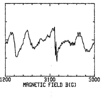
The EL2+ concentration of the sample is determined by electron paramagnetic resonance (EPR) spectroscopy from the arsenic antisite related quadruple EPR spectrum.13 The measurement is performed at a temperature of T=16 K un- der thermal equilibrium conditions. The sample shows only one EPR spectrum corresponding to the EL2 related arsenic antisite defect (Fig. 2). This spectrum is fully quenched by absorption in the intracenter transition at 1 pm. The spin Hamiltonian of the As&, defect, which is an electronic spin
S= l/2, nuclear spin I=3/2(100%) system is:
i’
I.
1200
3100
5006
HRGNETIC
FIELD 3(G)
FIG. 2. EPR spectrum of sample D2 showing the arsenic antisite related spectrum. 2~n$-~, kBT eok ‘= X cos 8 e l+k”/ki with S,[,EL2”]-S,[EL2+] 50=S,[EL20]+S,IEL2+] and
In these expressions no is the refractive index -of the
material (no=3.44 at 1.06 p, no=3.38 at 1.32 pm, and
n,=3.36 at 1.55 ~jg~lo; r41 is the electro-optic coefficient
(r 41=1.72 pm V-’ at 1.06 m, rb1=1.54 pm V-l at 1.32
,wm and r41 = 1.50 pm V-l at 1.55 prn),16 0 is the half-angle between the beams inside the crystal (we have for all grating
spacings cos &=l), E is the static dielectric constant
(E= 1.13X 10-l’ F rn-l.)l’
Q is the hole-electron competition coefficient and ki is the inverse squared of the Debye screening length. These parameters depend on the photoionization cross sections of carriers (S, for electrons and S, for holesj from the deep level EL2 (wavelength dependent parameter) and on the con- centration of the two state of charges of the EL2 defect (wavelength independent parameter).
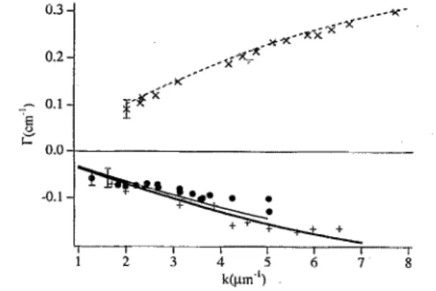
Experimentally we measure the energy transfer from a strong pump beam to a weak probe beam as a function of the grating spacing and deduce the photorefractive gain r (Fig. 3) .4J4 WC measure a change of the sign of the photorefractive
-O.l
i.
4 5 6 7.‘-.T
8kCm?
FIG. 3. Experimental (symbols) and theoretical (lines) photorefractive gain I? as a functionbf the grating wave number k for different wavelengths: (X) and dashed Iine forh? 1.06 /wn, (+) and bold straight line for X= 1.32 /*m, (0) and thin straight line for h=1.55 pm.
gain between 1.06 pm on the one hand and 1.32 and 1.55 pm on the other hand (Fig. 3). This means that Q is positive at 1.06 ,zrn (electron dominated photorefractive effect) and to is negative at 1.32 and 1.55 pm. (hole dominated photore- fractive effect). AU-the parameters that influence the theoreti- cal photorefractive gain are known, so we can compare our experimental results with the theoretical curves (Fig. 3). The accordance between experimental results and theoretical curves is good. It, particularly, well explains the change of sign of the gain between 1.06 ,zm, 1.32 pm, and 1.55 ,um.
In conclusion, using absorption and electron paramag- netic resonance measurements we determine the concentra- tion of the different states of charge of deep level EL2. These results and the known properties of the EL2 defect, allow us to calculate the photorefractive performance of undoped
GaAs. We show that the phototrefractive effect in undoped LEC GaAs can be quantitatively explained by the electron hole competition model with the single EL2 defect. Com- parison of theory and experiment is performed on the sensi-
tivity range (l-l.55 pm) of GaAs. We show that it extends
until 1.55 ,um, where photorefractive gains close to the ab-
sorption loss are obtained (I’wa=O.l cm-‘). The photore-
fractive effect in GaAs can thus be used as a contactless optical method of characterization of the compensation level of the EL2 defect, as performances around 1.3 ,um are very
sensitive to the [EL2’]/[EL2’] ratio.
‘Ph. Delaye, P. U. Halter, and G. Roosen, Appl. Phys. Lett. 57,360 (1990). ‘R S. Rana, D. D. Nolte, R. Steldt, and E. M. Monberg, J. Opt. Sot. Am.
B 9, 1614 (1992).
3J. C. Launay, V. Mazoyer, M. Tapiero, J. P. Zielinger, 2. GueUil, Ph. Delaye, and G. Roosen, Appl. Phys. A 55, 33 (1992).
4M. B. Klein, Opt. L&t. 9, 350 (19841.
*A. Partovi, E. M. Garmire, G. C. Valley, M. B. Klein, Appl. Phys. L&t. 55, 2701 (1989).
6E. J. Johnson, J. A. Kafalas, and R. W. Davies, J. Appl. Phys. 54, 204 (1983).
‘P. Silverberg, P. Omling, and L. Samuelson, Appl. Phys. Lett. 52, 1689 (1988).
‘F. X Zach and A. Wmnacker, Jpn. 3. Appl. Phys. 28,957 (1989). ‘D. T. E Marple, J. Appl. Phys. 35, 1241 (1964).
*‘J. S. Blakemore, J. Appl. Phys. 53, R123 (1982).
llK. Yamada, K. Watanabe, and K. Hoshikawa, Jpn. J. Appl. Phys. 28, L1686 (1989).
“G. M. Martin, Appl. Phys. L&t. 39, 747 (1981).
13R. J. Wagner, J. J. Krebs, G. H. Strauss, and A. M. White, Solid State Commun. 36, 15 (1980).
14N V Kukhtarev, V. B. Markov, S. G. Odulov, M. S. Soskin, and V. L. . . Vi&&ii, Ferroelectrics 22, 949 (1979).
lSF. P. Strohkendl, J. M. Jonathan, and R. W. Hellwarth, Opt. Lett. 11, 312 (1986).
16C. A. Berseth, C. Wuethrich, and F. K. Reinhart, J. Appl. Phys. 71, 2821 (1992).