Articles
https://doi.org/10.1038/s41566-020-0690-1Vectorized optoelectronic control and
metrology in a semiconductor
In the format provided by the authors and unedited
Supplementary information
Articles
https://doi.org/10.1038/s41566-020-0690-1Vectorized optoelectronic control and
metrology in a semiconductor
In the format provided by the authors and unedited
Supplementary information
Supplementary Information
Vectorized optoelectronic control and metrology in a semiconductor
Shawn Sederberg1,2,*, Fanqi Kong1, Felix Hufnagel3, Chunmei Zhang1, Ebrahim Karimi2,3, Paul B. Corkum1,2
1Joint Attosecond Science Laboratory, University of Ottawa and National Research Council Canada, 25 Templeton Street, Ottawa, ON K1N 6N5 Canada
2Max Planck - uOttawa Center for Extreme and Quantum Photonics, 25 Templeton Street, Ottawa, ON K1N 6N5 Canada
3Department of Physics, University of Ottawa, 25 Templeton Street, Ottawa, ON K1N 6N5 Canada *[email protected]
1 – Currents produced by coherent control
The relative phase between the fundamental and second harmonic can be used to control the momentum distribution in the conduction band. This “matter
interferometer,” depicted schematically in Fig. 1a, can be compared to an optical interferometer used to interfere light waves on a detector. In order to observe optical interference with the highest contrast, the intensity of light incident on the detector from each arm of the interferometer must be equal.
Similarly, in order to affect the greatest asymmetry on the momentum distribution in the conduction band, the contribution of ω and 2ω to the conduction band population must be balanced. In other words, we require:
𝛼𝐼!! = 𝛽𝐼!!,
where α is the linear absorption coefficient, I2ω is the second harmonic light intensity,
the extreme case where just one light frequency is used, the conduction band is populated symmetrically in momentum space and no net current is produced. When a second colour is introduced, quantum interference leads to an asymmetry in the momentum distribution of the conduction band population. “Balancing” the interferometer by using the appropriate combination of intensities produces the greatest asymmetry in the momentum distribution.
To relate this asymmetry to the observed current, it is helpful to consider the effect of electrons contained in an element dk about k in phase space. Such an element contains dk/4π3 electrons per unit volume, moving with a uniform velocity determined by the electronic band structure of GaAs:
𝐯 𝐤 = 1ℏ ∂ℇ 𝐤∂𝐤 , where ℇ 𝒌 is energy.
Integrating over the entire Brillouin zone, the current density can be written as: 𝒋 = 𝜌𝒗 = −𝑒 4𝜋! d𝒌 𝒗 𝒌 = −𝑒 4ℏ𝜋! d𝒌 𝜕ℇ 𝒌 𝜕𝒌
In the conventional case where the conduction band is populated with a symmetric momentum distribution, the current density vanishes since charges of equal amplitude travel in opposite directions. Any asymmetry in the momentum distribution of
conduction band electrons translates directly into a finite current density, which can be detected experimentally.
2 - Low temperature gallium arsenide (LT-GaAs) material
The commercially obtained LT-GaAs film (Xiamen Powerway Advanced Material Co., Ltd.) has a thickness of 1.2µm, a (100) surface orientation, and was grown on a 350µm thick GaAs substrate. The film is grown at 280∘C and annealed at 590∘C. The LT-GaAs film is crystalline, but has a relatively high density (>1018cm-3) of defects, including point defects at As antisites, As interstitials, and Ga vacancies1,2. These point defects act as recombination and trapping centers, and reduce the charge carrier lifetime to sub-picosecond durations3,4.
We characterise the charge carrier lifetime using a transient reflectivity set-up, whereby electron-hole (e-h) pairs are excited with an above-bandgap “pump” pulse at 𝜆 = 741 nm. The semiconductor plasma dynamics and the accompanying transient reflectivity of the material are measured using a strongly attenuated, non-collinear “probe” pulse at 𝜆 = 1482 nm, which is spatially overlapped with the 𝜆 = 741 nm pulse on the LT-GaAs substrate. The reflected probe pulse is spatially isolated and directed to an InGaAs photodetector, which is connected to a lock-in amplifier (Stanford Research Systems SR830). Adjusting the relative timing of the probe pulse with respect to the pump pulse enables measurement of reflectivity dynamics, which relate directly to the semiconductor plasma excitation and relaxation dynamics.
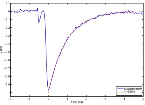
The result of this measurement is shown in Fig. S1. The sharp drop in reflectivity at 𝑡 = 0 ps results from the rapid excitation of e-h pairs in the semiconductor, where the semiconductor plasma reduces the effective refractive index of the material. As the e-h pairs recombine, the reflectivity recovers back to its original value. Fitting an exponential function to the recovery tail produces a
Fig. S1 | Transient reflectivity of LT-GaAs. Electron-hole (e-h) pairs are excited in
a LT-GaAs substrate using above bandgap 𝜆 = 741 nm laser pulses. The
semiconductor plasma reduces the refractive index, reducing the reflectivity of the substrate. The plasma excitation and recovery are probed by reflecting a weak, 𝜆 = 1482 nm laser pulse from the same spatial region of the substrate. Fitting an exponential function to the recovery tail reveals a recovery time constant of approximately 950 fs.
3 - Detector configuration
The detector assembly is a stack of two substrates: one substrate serves as a detection device, and the other as an optical mask. The detection device consists of a LT-GaAs film with two large aluminium electrodes separated by a gap of 25 µm patterned onto it, as shown in Figs. S2a,b. The mask is a fused silica substrate with the identical electrode configuration, presented in Figs. S2c,d. The two substrates are stacked vertically, and separated from one another by approximately 150 µm using smaller spacer substrates. Stacking the pair of substrates such that the two gaps are oriented
−2 −1 0 1 2 3 4 5 −1 −0.9 −0.8 −0.7 −0.6 −0.5 −0.4 −0.3 −0.2 −0.1 0 0.1 ∆ R/R Time (ps) Measurement τ r=950fs
orthogonally to one another forms a 25 µm × 25 µm aperture, limiting the exposed region of LT-GaAs to these dimensions. The stacked assembly is shown in Figs. S2e,f.
Fig. S2 | Schematic of apertured LT-GaAs detector. a, Top view of LT-GaAs
detection substrate with electrodes. b, Side view of LT-GaAs substrate with
electrodes. c, Top view of fused silica mask substrate. d, Side view of mask substrate.
e, Top view of assembled detector, where the fused silica substrate is not shown in
order to make the geometry more clear. f, Side view of the assembled detector.
4 - Optoelectronic detection
Quantum interference induced by the ω and 2ω laser beams imparts momentum to the photo-excited charge carriers. Electron momentum relaxation in GaAs occurs on a timescale of approximately 𝜏! = 180 fs 5, which is the timescale over which coherent transfer of electric charge is maintained. Rapid trapping of separated charges (i.e. e-h pairs) on a timescale similar to 𝜏! is essential for detecting a meaningful signal. Trapping separated charges in the LT-GaAs produces an electric dipole between the
electrode pair, which can be conceptually thought of as inserting a quasi-static dipole within a capacitor. The electrodes shield this dipole, driving a current through an external circuit, in this case a lock-in amplifier.
In the absence of rapid charge carrier trapping, space charging would bring conduction band electrons back to their host sites, and the temporal dynamics of the corresponding electron motion would exceed the bandwidth of modern electronic amplifiers, yielding no detectable signal. A natural question to ask is whether ballistic charge carrier transport from the semiconductor into the electrodes could also produce a meaningful signal? We investigate this question by fabricating similar detectors from silicon and GaAs, which have recombination timescales on the order of
nanoseconds or longer. The much faster timescales of charge carrier diffusion would hinder the formation of a quasi-static dipole within the semiconductor, and any detected signal would arise from ballistic charge carrier transfer into the electrodes.
Performing similar measurements with Si and GaAs detectors, and even greatly simplified measurements with Gaussian laser beams and large detector gaps, produced no detectable signal. However, performing measurements in LT-GaAs with a focal spot size significantly smaller than the electrode gap dimensions still produced a measureable signal. Therefore, we conclude that capacitive shielding of a trapped dipole is the primary signal that we detect, with minimal contribution from ballistic charge carrier transfer into the electrodes.
5 - Detection directionality
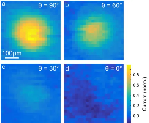
Sensitivity of the detection scheme to the direction of the local current is critical for resolving the x- and y-components of the current vector. Conventional Gaussian laser beams are used to measure the directionality of the detector, where the ω and 2ω laser
beams have identical polarisation. The detector begins in an orientation such that the polarisation of the laser beams is “across” the electrode gap, or at an angle of 90∘ with respect to the gap. The detector is raster-scanned across the laser beams and the current is recorded at each pixel. Leaving the laser beams unchanged, the detector is then rotated, and the measurement is repeated. The measurement is performed for angles of 90∘, 60∘, 30∘, and 0∘. Notably, the measurement at 0∘ is such that the polarisation of the two laser beams is aligned along the electrode gap, and any
currents would travel along the gap and not towards the electrodes. The result of these measurements is shown in Fig. S3. Clearly, the detected signal is strongest when the laser polarisation (and the resulting current) is oriented across the electrode gap. Any deviation from this configuration results in a decrease in the detected signal because the effective charge carrier separation in the direction of the electrodes is reduced. In the extreme case where the laser polarisation is aligned along the electrode gap, the signal is reduced by approximately an order of magnitude, similar to previous observations6,7. Therefore, the detector effectively isolates the component of the current that is aligned across the electrode gap.
6 - Current vector mapping
The directionality of the detector provides a natural means to isolate and detect one vector component of the current. Raster scanning the detector in one orientation would give access to one vector component, e.g. Ix. Rotating the detector 90∘ and repeating the raster scan then enables detection of Iy. The two measurements give full access to the transverse current amplitude and direction. Overlapping the intensity centre of mass of the two scans enables the current vector map to be plotted.
Fig. S3 | Directional sensitivity of current detector. Scans of the measured current
as the detector is raster scanned across ω/2ω Gaussian laser beams. The detector is rotated to a, 90∘ (laser polarisation is across the electrode gap), b, 60∘, c, 30∘, and d, 0∘ (laser polarisation is along the electrode gap).
7 - Rotational symmetry
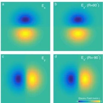
The azimuthal invariance of the laser modes under consideration enables the complete two-dimensional current vector mapping to be approximated from a single vector component. In Fig. S4, we illustrate that for a laser beam with azimuthal polarisation, the x-component of the electric field (Fig. S4a) is identical to its y-component after being rotated by 90o (Fig. S4b). Equivalently, the Ey component is the same as Ex after a rotation by -90o. The same relations are true for a beam with radial
polarisation, as shown in Fig. S5. Naturally, the two vector components of spatial current distributions representing either azimuthal or radial arrangements will be related in the same way. Since each current arrangement excited in the presented
measurements can be decomposed into a superposition of radial and azimuthal distributions, the full vectorial current arrangement can be approximated from just one vector component.
Fig. S4 | Rotational symmetry of azimuthal beam. The spatial distribution of the
x-component of the electric field, a, is identical to that of the y-x-component of the electric field, b, after its spatial arrangement has undergone a 90o rotation. Similarly, the spatial arrangement of Ey, c, is the same as that of Ex, d, once it has been rotated by -90o.
To quantify the applicability of symmetry under realistic experimental conditions, we perform a Pearson correlation analysis and a root mean square error (RMS error) analysis on a data set where both current components are available. Figure S6 shows the x-component (Fig. S6a) of the measured current presented in Fig. 3, along with the y-component of the measured current after rotating the data matrix by 90o (Fig. S6b). We calculate the Pearson correlation coefficient between these two
data sets to be 0.95, and the RMS error to be 4.9%. The minor differences between these two datasets are attributed to manual adjustment of the detector orientation, electronic detection noise, and imperfections in the optical setup.
Fig. S5 | Rotational symmetry of radial beam. The x-component of the electric
field, a, can be obtained by rotating the spatial arrangement of the y-component of the electric field, b, by 90o. Equivalently, the spatial arrangement of Ey, c, is identical to that of Ex, d, after it has undergone a -90o rotation.
8 - Raw data used for the production of Figure 5
The raw data for Iy used to produce Fig. 5 is shown in Fig. S7. The symmetry
relations presented in the previous section were applied to this data to approximate Ix. Exemplary current vector mappings are shown in Figs. 6a-d.The projection of the resulting current vector mapping onto the radial and azimuthal distributions was then calculated and used to produce Fig. 6e.
Fig. S6 | Testing symmetry using measured data. a,The x-component of the
azimuthal current, as presented in Fig. 3a. b,The y-component of azimuthal current shown in Fig. 3b after rotation by 90o.
Fig. S7 | Raw data used for the production of Figure 5. Each subfigure represents
the y-component of the detected current measured at the specified relative phase.
9 - Coherent control of magnetic fields using circular/radial
configuration
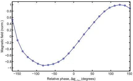
The raw data presented in Fig. S7 enables approximation of the full vectorial current distribution, which in turn enables calculation of the longitudinal magnetic field distribution via the Biot-Savart law. The longitudinal magnetic field distributions corresponding to the measured data in Fig. S7 are shown in Fig. S8. The magnetic field amplitude at the center of the distribution is plotted against the relative phase in
Fig. S9. Changing the relative phase modifies the relative strength of azimuthal and radial content in the excited current distribution. Because azimuthal currents produce a longitudinal magnetic field and radial currents do not, this has the effect of
modulating the longitudinal magnetic field amplitude and direction.
Fig. S8 | Magnetic field distributions corresponding to Figure 5. Applying the
symmetries described in Section 6 to the data for Fig. S7 enables calculation of the longitudinal magnetic field via the Biot-Savart law. These are shown in a-x, where the relative phase is denoted in each subfigure.
Fig. S9 | Coherent control of magnetic fields. The magnetic field at the centre of the
distributions shown in Fig. S8 is plotted versus the relative phase between the ω and 2ω beams. −150 −100 −50 0 50 100 150 −1 −0.8 −0.6 −0.4 −0.2 0 0.2 0.4 0.6 0.8 1 Magnet ic field (norm. )
10 - Spectral and temporal characterization of optical sources
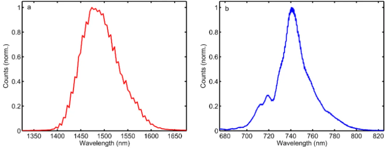
The measured spectrum of the ω pulse is shown in Fig. S10a, and is centred at 𝜆 = 1482 nm. Frequency doubling these pulses in a beta-barium borate crystal produces the spectrum plotted in Fig S10b, with a peak amplitude at 𝜆 = 741 nm.Fig. S10 | Measured spectra. a, Spectrum of fundamental pulses centred at
𝜆 = 1482 nm, measured with a grating spectrometer. b, Spectrum of second-harmonic pulses centred at 𝜆 = 741 nm.
While the spectrum provides some insight into the pulses used, important details are contained in the precise waveform of the laser pulses, i.e. the temporal intensity envelope and the temporal phase. To obtain these details, we perform frequency-resolved optical gating (FROG) measurements on each of the pulses after they have passed through the experimental setup.
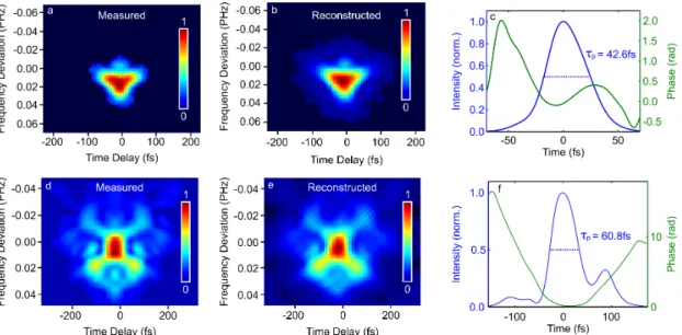
The measured and reconstructed FROG traces for the fundamental laser pulses are shown in Figs. S11a and b, respectively. The intensity envelope and temporal phase are presented in Fig. S11c. The pulse duration is 𝜏! = 42.6 fs, and is relatively well compressed with only minor third-order dispersion present.
Fig. S11 | Frequency-resolved optical gating (FROG) measurements. a, Measured
and b, reconstructed FROG traces of fundamental laser pulses at 𝜆 = 1482 nm. c, Temporal intensity envelope and temporal phase of fundamental laser pulses, demonstrating a duration of 𝜏! = 42.6 fs. d, Measured and e, reconstructed FROG traces of second-harmonic laser pulses at 𝜆 = 741 nm. f, Temporal envelope and phase of the second-harmonic pulses lasting 𝜏! = 60.8 fs.
Measured and reconstructed FROG traces for the second-harmonic pulses are shown in Figs. S11d and e, respectively. The temporal characteristics of the pulse are plotted in Fig. S11f. Notably, this pulse is slightly longer, with a duration of
𝜏! = 60.8 fs and substantial second-order dispersion. A combination of group-velocity mismatch in the second-harmonic generation crystal and stronger dispersion in transmissive optical components stretch the pulse and impart it with a slightly more complicated intensity envelope. Nevertheless, the pulse is well behaved and suitable for coherent control measurements.
11 - Estimation of conduction band population
Using the measured mode profile shown in Fig. 2b together with the temporal intensity envelopes shown in Figs. S11c,f, we estimate the peak intensity of the fundamental pulse to be approximately 𝐼!,! = 6.69×10! W/cm2and that of the second harmonic pulse to be 𝐼!,!! = 7.75×10! W/cm2. Conduction band population dynamics can be calculated using the following differential equation:
𝑁 = 1
2ℏ𝜔 𝛼𝐼!!+ 𝛽 𝐼! ! − 𝐷!∇!𝑁 − 𝑁 𝜏!
where 𝑁 is the conduction band population, ℏ is the reduced Planck constant,
𝛼 = 1.808×10! cm!! is the linear absorption coefficient, 𝛽 = 5 cm/GW is the two-photon absorption coefficient, 𝐷! is the ambipolar diffusion coefficient, and
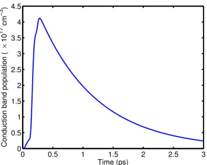
𝜏! = 950 fs is the charge carrier recombination time. Due to the rapid charge carrier recombination of the present material, we neglect charge carrier diffusion in our analysis. Applying the intensity envelopes of Figs. S11c,f to Eq. (1), we calculate the conduction band population dynamics, which are shown in Fig. S12. The conduction band population increases rapidly, with the majority of the population being injected on the timescale of the main pulse of the second harmonic. After the laser pulses have ended, the conduction band population decays with the characteristic timescale, 𝜏!. The peak conduction band population is estimated to be 4.1×10!" cm!!.
Fig. S12 | Conduction band population dynamics. Simulated conduction band
population as a function of time. The rapid increase in the conduction band population approximately follows the duration of the laser pulses. The exponential decay follows the recombination timescale of the LT-GaAs material.
12 - Fabrication of q-plates
The q-plate used in the experiment is a type of Pancharatnam-Berry Optical Element (PBOE) which allows for the introduction of a transverse phase profile by adding a position dependent geometric phase8. The space-varying control of the phase is achieved by controlling the orientation of the liquid crystal in the plate. The q = 1/2 plate can be used to create beams carrying orbital angular momentum from circularly polarised Gaussian beams. When linearly polarised light is used, the result is instead a vector mode, where the orientation of the input linear polarisation defines a different set of vector modes. An azobenzene dye (in our case PAA7/6/20-22) is spin-coated on a pair of indium tin oxide (ITO) glass plates. The PAAD-22 dye has an absorption peak in the ultra violate, thus we use a 405 nm laser for the photoalignment of the
0 0.5 1 1.5 2 2.5 3 0 0.5 1 1.5 2 2.5 3 3.5 4 4.5 Time (ps)
Conduction band population (
× 10
17
cm
−
azobenzene molecules along the polarisation axis of the laser beam. To achieve spatially dependent orientation for the azobenzene molecules, a digital micromirror device (DMD) in conjunction with a half-wave plate selects the region being
illuminated and the desired polarisation orientation. The liquid crystal is introduced to the cell through capillary action, and then the cell is sealed.
13 – Lock-in Amplification
Lock-in amplifiers enable signals well below the electronic noise floor to be accurately detected and amplified. The key feature of lock-in amplification that enables this is phase-sensitive detection, which requires a reference frequency. In the present case, laser pulses at ω and 2ω are used to excite a semiconductor with
integrated electrodes. While the repetition rate of the laser can serve as a reference frequency, unwanted electrical signals arising from intense light irradiating the metal-semiconductor junction can introduce artifacts to the measured data. To this end, it is beneficial to amplitude modulate the weak, 2ω signal using an optical chopper that allows every second 2ω laser pulse to pass. In this scheme, the chopper frequency (i.e. half of the laser repetition rate) is used as a reference frequency for the lock-in amplifier.
The lock-in amplifier takes this reference waveform and generates an ideal sinusoidal waveform at the reference frequency using a phase-locked loop, Vref(t) =
V1sin(ωreft + θref). When an electrical signal, Vsig(t), is input to the lock-in amplifier, it is first amplified and then multiplied it by Vref(t). Given that Vsig(t) is periodic in time, it can be expanded as a Fourier series:
𝑽𝒔𝒊𝒈 𝒕 = 𝒂𝟎+ 𝒂𝒏𝐜𝐨𝐬 𝒏𝝎𝒕 ! 𝒏!𝟏 + 𝒃𝒏𝐬𝐢𝐧 𝒏𝝎𝒕 ! 𝒏!𝟏 ,
where an and bn are the real-valued coefficients of the expansion. Multiplying the reference waveform with just one term of this expansion, Vsig,b1(t) = b1sin(ωt) enables application of simple trigonometric identities:
𝑽𝒔𝒊𝒈,𝒃𝟏 𝒕 ⋅ 𝑽𝒓𝒆𝒇 𝒕 = 𝒃𝟏𝐬𝐢𝐧 𝝎𝒕 ⋅ 𝑽𝟏𝐬𝐢𝐧 𝝎𝒓𝒆𝒇𝒕 + 𝜽𝒓𝒆𝒇
=𝟏
𝟐𝒃𝟏𝑽𝟏 𝒄𝒐𝒔 𝝎 − 𝝎𝒓𝒆𝒇 𝒕 − 𝜽𝒓𝒆𝒇 − 𝒄𝒐𝒔 𝝎 + 𝝎𝒓𝒆𝒇 𝒕 + 𝜽𝒓𝒆𝒇
The result is a signal with frequency content at (ω – ωref) and (ω + ωref). In the case where ωref = ω, the frequencies are approximately DC and 2ω. Passing this signal through a low-pass filter isolates the DC signal, where the detected signal is approximately Vdet = ½b1V1cos(θref). This signal is proportional to the input signal amplitude, and has a maximum amplitude when the reference signal and detected signal are in phase, i.e. θref = 0. A similar analysis can be performed for all higher-order terms of the Fourier series expansion, but it is easy to show that they do not contribute to the detected signal because they are blocked by the low-pass filter. Similarly, the vast majority of electronic noise is blocked by the low-pass filter simply because its phase is inherently random.
References
1. Kaminska, M., Lilienthal-Weber, Weber, E. R., George, T. Kortright, J. B., Smith, F. W., Tsaur, B.-Y., & Calawa, A. R. Structural properties of As-rich GaAs grown by molecular beam epitaxy at low temperatures. Appl. Phys. Lett. 54, 1881-1883 (1989).
2. Matyi, R. J., Melloch, M. R., & Woodall, J. M. Structural analysis of as-deposited and annealed low-temperature gallium arsenide. J. Cryst. Growth 129, 719-727 (1993).
3. Gupta, S., Frankel, M. Y., Valdmanis, J. A., Whitaker, J. F., Smith, F. W., & Calawa, A. R. Subpicosecond carrier lifetime in GaAs grown by molecular beam epitaxy at low temperatures. Appl. Phys. Lett. 59, 3276-3278 (1991).
4. Liliental-Weber, Z., Cheng, H. J., Gupta, S., Whitaker, J., Nichols, K., & Smith, F. W. Structure and carrier lifetime in LT-GaAs. J. Electron. Mater. 22, 1465-1469 (1993).
5. Leitenstorfer, A., Fürst, C., Laubereau, A., & Kaiser, W. Femtosecond carrier dynamics in GaAs far from equilibrium. Phys. Rev. Lett. 76, 1545-1549 (1996). 6. Haché, A., Sipe, J. E., & van Driel, H. M. Quantum interference control of
electrical currents in GaAs. IEEE J. Quantum Electron. 34, 1144-1154 (1998). 7. Schiffrin, A. et al. Optical-field-induced currents in dielectrics. Nature 493, 70-74
(2013).
8. Larocque, H. et al. Arbitrary optical wavefront shaping via spin-to-orbit coupling,