Development of an Implantable Sensor for Continuous
Real-time Long-term Monitoring of
Soft Tissue Biomechanics
by
Zijun Wei
Submitted to the Program in Media Arts and Sciences, School of Architecture and Planning,
in partial fulfillment of the requirements for the degree of Master of Science
at the Massachusetts Institute of Technology
June 2018
Massachusetts Institute of Technology 2018. All rights reserved.
Signature redacted
Zijun Wei 7 Program in Media Arts and Sciences
Certified by
Signature red acted
Dr. Canan Dagdeviren Assistant Professor, MIT Media Lab
Approved by MASSACHUSETTS INSTITUTE MASSACHSET ILNSTITUTE OF TECHNOLOGY
JUN 2
7
2018
LIBRARIES
? -Thesis SupervisorSignature
redacted-Tod Machover Academic Head, Program in Media Arts and SciencesDevelopment of an Implantable Sensor for Continuous Real-time Long-term Monitoring of
Soft Tissue Biomechanics
By Zijun Wei
Submitted to the Program in Media Arts and Sciences, School of Architecture and Planning,
on May 4, 2018
in partial fulfillment of the requirements for the degree of Master of Science
Abstract
Measuring the mechanical properties of soft tissue can be an important method to detect pathology. Concerning the brain in particular, correlation between abnormal tissue stiffness and morbidity has been reported for Alzheimer's disease, Parkinson's disease and brain tumors, among others. On a more fundamental level, the nature and behavior of the brain from a mechanical standpoint is relatively understudied, in comparison to those from the chemical, electromagnetic and optical perspective. Current techniques fall into two main categories: one establishes direct contact to measure the deformation of tissue under various mechanical loads, the other solves the inverse problem based on the tissue displacement data collected through a number of imaging modalities. Both categories, however, have their limitations in providing ideal mechanical measurement of the brain, ranging from form factor compatibility, spatiotemporal resolution and accuracy. In this light, this work aims at developing an implantable measurement device that can bypass these limitations and provide in situ, in vivo, real-time, long-term monitoring of soft tissue biomechanics. The initial goal is to create a functional sensor front-end that can differentiate materials of different stiffness. As this project is to continue beyond the thesis, this thesis will present the current development progress, issues encountered and
corresponding counter-measures, and discuss the prospective work in the future.
The following people served as thesis readers of this thesis:
Thesis reader
Signature redacted
Dr. Edward S. Boyden Associate Professor, MIT Media Lab and McGovern Institute, Departments of Biological Engineering and Brain and Cognitive Sciences
Thesis reader
Signature redacted
Dr. Steve Ramirez Assistant Professor, Department of Psychological and Brain Sciences, Boston University
TABLE OF CONTENTS
SOverview ... 7
1.1 Introduction ... 7
1.2 M otivation and target problem ... 8
1.3 Direct contact approach ... 9
1.4 Indirect approach...9
1.5 Approach to follow ... 10
1.6 Prospective contributions...11
2 M aterial Theory and Device Concept ... 13
2.1 Overview of piezoelectricity ... 13
2.2 M aterial Selection ... 17
2.3 Actuator-sensor pair working m echanism ... 18
3 Testing M ethodology ... 21
3.1 Piezoelectric M aterial Testing...21
3.1.1 Polarization-electric field graph... 21
3.1.2 How to obtain a PE graph experim entally... 22
3.2 Voltage-Dis place m e nt Test ... 25
3.3 Actuator-Sensor Pair Response ... 26
4 Design and Fabrication Iterations ... 28
4.1 Design Overview ... 28
4.2 Fabrication Process...29
4.3.1 Design 01 (D1)...33
4.3.2 Design 02 (D2)...44
4.3.3 Design 03 (D3)...68
5 Issues encountered in the development process ... 70
5.1 Issues in fabrication process ... 70
5.1.1 HF etching of SiO2 for releasing PZT capacitors... 70
5.1.2 PZT deterioration during high-tem perature PI curing ... 75
5.2 Issue in characterization equipm ent configuration ... 76
6 Future W ork and Testing Plan ... 80
6 .1 D 3 te st ... 8 0 6.1.1 M aterial test...80
6.1.2 Actuator-sensor response test... 80
6.2 New material selection ... 81
6.2.1 Lead-free piezoelectric material ... 81
6.2.2 Optimal material for the actuator and sensor... 81
7 Acknowledgements...84 8 B ib lio g ra p hy ... 8 5
1
OVERVIEW
1.1 Introduction
Characterizing the mechanical properties of soft tissue has been an effective measure for disease diagnostics. For instance, difference in local mechanical properties in organs such as lung, prostate, breast and brain-, is used as a pathological signature in various methods that are currently in clinical application.
The technologies available today to assess soft tissue mechanics fall into two basic categories: 1) indirect approach based on various imaging techniques and 2) direct-contact approach. The first category features elastography, the most representative of which are ultrasound elastography5 and magnetic resonance elastography6. These are the standard methods of today's clinical application. However, such procedure is mostly time-consuming, costly and requires cumbersome operational setting and bulky equipment. Moreover, they are unsuitable for continuous real-time, long-term monitoring and can only provide relative measurement. The second category involves classical methods of compression, tension and indentation, which are suitable for research laboratory setting, but difficult for real-time, long-term clinical applications on human subjects.
In lights of these existing techniques, this thesis work is aimed at developing an implantable mechanical sensor that can potentially overcome their respective deficits and serve as a long-term measurement platform that can aid clinical treatment evaluation. As this project is to continue beyond the timeline of this thesis, this work will be a summary of current progress and description of upcoming work in the future.
This thesis will be organized as follows. Section 1 gives a brief review of current techniques for soft tissue mechanical characterization. Section 2 discusses the principle of the proposed device. Section 3 describes the testing methodologies. Section 4 presents the prototype designs, followed by discussion of the fabrication processes and preliminary test results. Section 5 and 6 summarize the issues encountered in the development process and discuss future work.
1.2 Motivation and target problem
Novel techniques are necessary for extracting pathological signature of brain diseases by measuring the biomechanics of brain tissues. Thousands of Americans suffer from the debilitating effects and even mortality of brain diseases, such as multiple sclerosis and tumors. For brain tumors alone, 79,270 new cases are expected to be diagnosed in the
US in 20177, with an estimate of 16,947 deaths to be attributed to primary malignant brain
and other central nervous system tumors. Many brain diseases, including sclerosis, tumors, hydrocephalus, and Alzheimer's disease, are accompanied by changes in the mechanical properties of specific brain tissues8-1 0. Meningioma, a common type of brain tumor, has been reported to have an average Young's modulus of 33.1 kPa, as compared to 7.3 kPa of normal brain tissue8. On the other hand, a study has shown that certain brain regions of people with probable Alzheimer's disease have lower median shear stiffness of 2.20 kPa, in contrast to 3.07 kPa for normal people4. Thus, mechanical property change in brain tissue is an important indicator of pathological progression. Using the mechanical signature as a reference to guide brain diseases diagnosis is, therefore, particularly imperative.
The specifications of an ideal technique are determined by the nature of brain tissue and characteristics of the associated diseases. Brain tissues exhibit different mechanical properties under in vivo and ex vivo conditions1 1 2, and are non-homogeneous in general13. To acquire clinically valid data for diagnosis and treatment guidance, therefore, necessitates an in vivo technique with high temporal and spatial resolution. Some diseases such as unresctable brain tumors and cancer metastasis1 4
-1 require
radio/chemotherapies over a duration of time. To monitor the effect of treatment to these diseases entails the capability of continuous real-time long-term operation. Additionally, for diseases involving subcortical regions 20,21, deep-brain access with minimal to none invasiveness is desirable. No current technologies can fulfill all of these requirements simultaneously.
1.3 Direct contact approach
There have been multiple reports of using the conventional testing methods, such as those for tension, compression, torsion and creep tests to characterize the mechanical properties of brain tissue. Early studies were mainly in ex vivo settings, using equipment designed for hard materials, and assessing brain tissue through direct contact2 2-26
.
Specifically-designed devices were also used to conduct the indentation tests on animal models in vivO2728.
These methods at present are limited mainly by their large form-factor. While indentation tests with custom made platform have already been demonstrated on in vivo animal
models27
,28, the setup reported in the study is bulky for clinical applications on humans. Other techniques such as palpation and handheld indentation probe29, while less bulky,
are still not suitable for accessing deep-brain regions without major surgery and can only be applied intraoperatively, thus not compatible with continuous long-term monitoring.
1.4 Indirect approach
With the introduction of advanced imaging techniques, particularly ultrasound30 and
magnetic resonance imaging (MRI)31, a derivative technique called elastography,
provides indirect, non-invasive, in vivo assessment of brain tissue mechanics. It includes two main subcategories: the first one is magnetic resonance elastography6, MRE, based
on MRI. The second one is sonoelastography (SEL)5,32 based on ultrasound imaging.
They have been in clinical use for over a decade, generating numerous data for reference. Elastography relies on inversion algorithms to deduce the moduli of tissue32
,33. The underlying assumptions for these algorithms, adopted for simplification or to reduce computation intensity, introduce measurement error or neglect certain essential mechanical properties all together6,32. The indirect nature and currently non-standardized protocols of elastography can lead to non-unified results, as exemplified by variations in data across different studies using the same actuation frequencies 3 4a0. This means that
elastography can only provide relative values, the accuracy of which, as compared to results from standard mechanical testers, needs to be validated with an in situ in vivo technique. Noteworthy is the operator-dependent propensity of the imaging techniques, particularly ultrasonography4' 42, which can also add to the variations in elastography data. The long scan time and post-scan inversion processing, which typically takes about 10 minutes for MRE, also inhibit the application of MRE in a continuous real-time fashion. In addition, the spatial resolution of elastography, which is usually lower than that of their underlying imaging technique6,43, lies in the millimeter range even with the best
technologies currently available44-46. Although high spatial resolution in the range of 200x200 pm2 has been achieved with 7T MRI, this resolution requires long scan time and is sensitive to motion artifacts and other noises, which is difficult to achieve with patients. Furthermore, the strong magnetic field applied dictate its inapplicability on patients with metal implants (e.g. pacemaker). There is also the concern that the equipment setup can cause emotional distress for claustrophobic subjects47. As for ultrasound, even though the most advanced SEL technology can provide real-time data at a considerable depth48, non-invasive transcranial ultrasound can only be applied through four "acoustic window" on the sku1149-51, which may be insufficient or absent in patients with thick bones5 2. This
limits the applicability of non-invasive transcranial ultrasound, let alone SEL. Besides, the cost and form-factor still makes its application in continuous long-term monitoring impossible.
1.5 Approach to follow
In 2015, an article reported a conformal modulus sensor (CMS)53 that can be used to
characterize the moduli of human skins. This sensor is composed of an array of piezoelectric capacitors. Half of these capacitors were designed as piezoelectric actuator, while the others were designed as sensor. By applying a harmonic driving voltage to the actuator and measuring the AC voltage response across the sensor, the authors reported a correlation between the sensor output voltage and the stiffness of the materials that the
able to measure the relative stiffness of a variety of soft tissues ex vivo and human skin tissue in vivo.
The low-form factor and its nature of establishing a direct contact of such device architecture make it a promising candidate for circumventing the abovementioned deficits of both the conventional direct-contact method and the imaging-based indirect method. And it is this device architecture that this thesis work takes as a starting point towards a fully implantable modulus measurement platform.
In 2018, a thin film moduli sensor with a similar device architecture was reported to be able to guide biopsy needle (BN)54 positioning. The study was conducted on an in vivo mouse model and tissues from various internal organs such as lung, liver and kidney ex
vivo. This yet again substantiates the validity of this device architecture.
1.6 Prospective contributions
Elastography, particularly MRE, is still an emerging technique. Some studies have investigated the mutual validation of MR elastography and ultrasound elastography55,56,
but with both elastography modalities being an indirect imaging-based method, a third independent criterion capable of in situ, in vivo measurement, such as the implementation of the proposed sensor can be beneficial for this evaluation.
More data from a greater variety of modalities can benefit the clinical research on brain disorder and tumors. On a more fundamental level, whereas the chemical, electric, magnetic and optical modalities have been intensively explored and developed, the mechanical modality to examine the nature and behavior of brain tissue is relatively understudied. The proposed sensor with the functionality for in situ in vivo continuous real-time long-term moduli monitoring can add to our current knowledge of brain tissue from a biomechanics perspective.
Radio- or chemotherapy usually spans over a relatively long period of time. A typical fractionated radiotherapy, for example, can last from 20 to 60 days5 7 5 8. As imaging can
contrast, the proposed device can benefit concurrent assessment of such treatment as radio-, chemo- and immunotherapy, and allow medical professionals to make timely adjustment in treatment strategies.
Additionally, development of this sensor can circumvent many of the limitations facing the currently available techniques. By establishing direct contact with the tissue, the sensor can bypass the interference coming from the skull or overlaying tissues that may introduce errors to the results of MRE and SEL. The reduced form factor of this microfabricated sensor will enable its access to deep-brain region without causing significant tissue damage, as compared to existing direct-contact methods. The proximity of the actuator and sensor will allow for actuation with lower amplitude and higher frequency, hence causing less disturbance to the normal functioning of brain tissues and achieving higher spatial resolution, down to micrometer level. Such down-scaling and localization of power distributed and dissipated within brain tissue can also reduce the risk of tissue heating and damage, which can be the concern of ultrosonography59. All these features will enable its application in in situ in vivo continuous real-time long-term monitoring of brain tissue.
2 MATERIAL THEORY AND DEVICE CONCEPT
2.1 Overview of piezoelectricity
Piezoelectricity refers to the accumulation of charge at the surface of a material under external stress. It was first discovered in late 1 9th century by The Curie Brothers in quartzO0.
This phenomenon is also called the direct piezoelectric effect, as opposed to the converse piezoelectric effect, which refers to the deformation of a material under an external electric field. These two reciprocal effects are closely related the concept of polarization, which is the separation of different charges within a dielectric (insulator). The physical quantity polarization density is defined as the volumetric/areal density of electric dipole moments due to this separation within the material.
Upon application of an external electric field, the negative and positive charges within an electrically-neutral dielectric material are separated along the field direction, and thus creating electric dipole moments between them. This process is called dielectric polarization, described by the parameter electric susceptibility, and is applicable to all dielectric materials. The dipole moments thus created are called induced dipoles.
A certain class of material, although macroscopically neutral, possesses electric dipoles
even without an external electric field. This is called spontaneous polarization.
Microscopically, piezoelectricity relies on the coupling of re-orientation of these induced or spontaneous dipole moments with the crystal structure, under the condition of external electric field or stress field. Unlike polarization, the presence of this coupling is not ubiquitous among dielectrics, and is determined by the crystal structure of the material.
Of the 32 crystallographic point groups that can describe all materials, 21 are
non-centrosymmetric, of which, 20 exhibit piezoelectric properties. Among these 20, 10 pyroelectric point groups possess spontaneous polarization dipoles, and if these dipoles form domains, regions where all dipoles are aligned, that can be switched by electric field, the materials are called ferroelectric61.
For polycrystalline ferrorelectric material (for example, ceramic films), each grain behaves like a single crystal and has multiple domains. If these domains are randomly oriented,
the overall polarization density of the material is very close, if not equal to zero; on the other hand, if there is a preferred orientation of these domains across all crystal grains, the material will have a non-zero polarization, and the polycrystalline material is thus called "poled".
Going back to the macroscopic scale, where piezoelectric effects were first discovered and find most applications, these effects can be succinctly described by two constitutive equations. The first one relates the electric displacement field vector [D] in the material to the externally-applied stress matrix [T] through a piezoelectric coefficient matrix
[d]Eand corresponds to the direct piezoelectric effect:
[D] = [d]E.I[T] (.a)
The electric displacement field, with a dimension of areal charge concentration
[F
=[-],
describes the density of stress-induced charges. Adding in the effect of an external electric field vector[E] from the electromagnetic definition of D gives us:[D] = [d]E . [T + [E] -[E] (1 b)
where [e] is the material permittivity matrix, and the superscript E refers to keeping the external electric field constant.
The complete form for a piezoelectric material with in-plane symmetry perpendicular to the poled (polarization) direction (defined as axis-3, the other two directions defined as
1 and 2): D1l 0 0 0 0 d15E 022 0 0 0 dlsE 0 T0133 + 0 E22 0 2 C) D3 d3 1E d3 3E 0 0 o T23 0 0 E33- E3 I 0 -T31
T12-where for D and E, subscript 1,2,3 refers to the respective components; for dE and E, which are effectively conversion coefficients, the first number in the subscript describes the direction of the resultant variable, and the second number describes the direction of
displacement component in direction 1(2) induced by the shear stress in the 23 or 31 plane. dEhas a dimension of[-]. And for vector T, components with two identical numbers as subscript refer to the normal stress along the specified axis, components with different numbers as subscript refer to shear stress on the corresponding planes.
dEhas a dimension of[c], and is called charge-stress constant.
The second equation, likewise, relates the strain field vector [S] in the material to an external electric field vector[E], and corresponds to the converse piezoelectric effect:
[S] = [d] - [E] (2a)
The strain field describes the axial deformation of the material, and adding in the effect of external stress from Hook's Law gives us:
[S] = [c] -[T] + [d]T . [E] (2b)
where [c] is the compliance matrix of the material, and the superscript T refers to keeping the external stress constant.
The complete form for a piezoelectric material with in-plane symmetry perpendicular to the direction of polarization:
S11 -C1 1 C1 2 C13 0 0 0 - -T 0 0 d3 1T S22 C1 2 C11 C1 3 0 0 0 T2 2 0 0 d3 1T S3 3 _ C1 3 C13 C3 3 0 0 0 T33 + 0 0 d33 E (2c) 2S2 3 0 0 0 C 4 4 0 0 T23 0 d1 5T 0 E3J 2S31 0 0 0 0 c55 0 T3 1 d1 5T 0 0 .2S12- 0 0 0 0 0 c6 6 - 1 2- 0 0 0
where the subscript convention is the same as equation (1) for T, dT, E, with S following
the convention of T, and c following the convention of dT, with the exception of ci1(i =
4,5,6), which corresponding to the respective shear stress-strain relations.
A piezoelectric sensor which converts stress to voltage/charge can be readily described by equation (1), and the displacement field is related to the generated charge by the
relation6 2:
rdA i]
Q=ff[Dl D2 D3] dA2 (3) LdA3]
where dAi(i = 1,2,3)is the differential area on the plane, or on experimental terms, the
surface electrode, normal to the corresponding axis.
A piezoelectric actuator which deforms under external electric field can be described by
equation (2).
For a polycrystalline piezoelectric ceramic thin film poled along the top surface normal, a schematic is shown below.
3
2
1
Figure 2.1.1. A polycrystalline piezoelectric thin film poled along the surface normal. Each yellow arrow represents the domain of a single grain. While not all domains can be aligned with one direction, the poled direction is the direction of the total polarization dipole moment within the film, i.e. the vector sum of polarization dipoles of all the grains. Axis 3 is defined as along the poled direction, and axis 1 and 2 are defined as in-plane.
When the film is used as an actuator, under an external electric field along the poled direction, the induced strain along the same direction is called strain in d33 (longitudinal/ thickness) mode, and that in the plane of the thin film is called strain in d31 (transverse/in-plane) mode. The reciprocal process, when the film is used as a sensor, the electric
field/charge induced along the poled direction is called field/charge generated in d33 or d31 mode, if it is caused by stress along or perpendicular to the poled direction.
D33 mode
Polarization direction
D31 mode
Figure 2.1.2 d33 and d31 deformation mode of a piezoelectric thin film under AC voltage
2.2 Material Selection
Since the discovery of piezoelectric effect, there have been continuous research efforts in putting piezoelectric materials into application as well as in finding new materials with superior piezoelectric properties. The past century has seen the military adaptation of quartz in sonars for submarine detection, later to be replaced by the lead-based ceramics system, which has since taken a major role in modern industry, ranging from the controller in an ink-jet cartridge, to the transducer in ultrasound imaging probe. With regulations established towards a more environmentally-friendly industry6 3, the lead-based system is
expected to be substituted for lead-free piezoelectric materials.
As lead zirconate titanate (PZT) has been a widely used piezoelectric/ferroelectric ceramic system, also the reference works5
3,54 have used this material to demonstrate
their system, this thesis work has chosen PZT as the initial material for prototyping. PZT is a solid solution of two oxides, PbZrO3 and PbTiO3, and takes the general formula
of Pb(Zr1 _xTix)O3. By changing x and the temperature, PZT can go into different phases,
which greatly affects its piezoelectric properties64.
It has been reported in the literature that pure PZT solid solution exhibits piezoelectric properties most prominently at its morphotropic phase boundary (MPB)65 between the
ferroelectric rhombohedral phase and the ferroelectric tetragonal phase, which at room temperature is near the Zr :Ti ratio of 52:48. This ratio is chosen as the composition ratio for the PZT material used in this work.
For application of the piezoelectric material as actuator and sensor, it is necessary to have electrical access to the thin film. Platinum is a common choice as the bottom electrode, as it has a close lattice constant to that of PZT and tends to form a highly textured film with (111) orientation, which in turn can induce PZT film to follow the same orientation66. As have been reported67, having a thin layer Titanium (Ti) below the Pt can enhance this texture of PZT film, as Ti can infuse through the Pt, be oxidized and serve as the nucleation site during PZT annealing. Therefore, the stack Si/SiO2/Ti/Pt is chosen.
For the application of a low form-factor device, thin film is chosen instead of ceramic blocks. Further, to take advantage of the established industry of PZT processing, the above thin film is prepared by a thin film manufacturer, KCMC. A schematic of the thin film stacks with respective thickness information is given in Figure 2.2.2.
The Pt thin film is confirmed by X-ray Diffractometry to have (111) orientation, and the PZT thin film on top of it exhibits a preferred orientation of (111).
PZT(500nm) Pt(100nm)
Ti(5nm) Si02(600nm)
Si
Figure 2.2.1 Thin film stack prepared by KCMC
2.3 Actuator-sensor pair working mechanism
Having an actuator-sensor pair is essentially decomposing an acoustic transducer. Unlike a conventional direct measurement method, where the external force and material displacement are recorded and converted to a stress-strain relation for extraction of modulus, the piezoelectric actuator-sensor pair functions like tomography, in the sense
that a wave is generated from a source (vibration due to a driving voltage), propagating through the medium of interest, and then received as signal from which the properties of the transmitting medium is back-calculated.
On the other hand, unlike elastography, which has no measure of local stress, the piezoelectric actuator-sensor pair can control local stress since the miniaturized actuator is in direct contact with the tissue to be examined. Nonetheless, whereas stress-strain/force-displacement graph reflects tissue moduli straightforwardly, and elastography inversion algorithms have been intensively studied with established framework already in application, the actuator-sensor pair architecture is yet to have a description of working mechanism to the same level of completeness. The two major publications describing modulus measurement using this mechanism give semi-empirical models that are only explanatory for the particular experiments.
In the CMS article, the proposed quasi-static model takes into account the strain transfer from the actuator to the medium, the stress transfer from the medium to the sensor, and the transmission of this stress through the medium. For the third process in particular, a fracture mechanics model is adopted based on experimental results, to obtained a linear scaling factor between the stress at the actuator and that at the sensor.
This model assumes that the elastomeric substrate of the device has achieved seamless contact with the in vitro gel model or the tissue of interest. When a voltage is applied to the actuator, the vertical expansion due to d33 deformation of piezoelectric capacitor stack creates gaps between the material and elastomeric substrate, which are modeled as cracks. The transmission of stress from actuator to sensor is solved with the force equilibrium condition for the cracks to be held close, as detailed in a follow-up article by the original authors68. Another article published a year later69 revisited the modeling of
the skin modulus sensor. It is remarkable that in this article coauthored by original authors, the fracture mechanics model adopted specifically to explain the CMS in the original article is not mentioned. Instead of d33 thickness deformation mode, the d31 in-plane
deformation mode is considered dominant, and the analysis is presented in elastic wave propagation formalism.
In the BN article5 4, a scaling law is presented based on finite element analysis(FEA). This
scaling law can capture the trend between the modulus of the material and the sensor output under a specific set of conditions regarding device dimension and substrate modulus relative to that of target tissue. Nevertheless, it is a numerical formula that does not directly reflects the mechanics, and given the limitations above, it is case-specific. Additionally, whereas CMS model considers the thickness vibration mode d33 as the major mode and neglect the in-plane vibration d31, the scaling law proposed in the BN does the
opposite and regards d31 mode as the major part.
In this light, there have not been a unified theoretical model to describe the working mechanism of a piezoelectric actuator-sensor pair in measuring tissue biomechanics. Noteworthy is that there have been analytical and numerical studies on surface bonded piezoelectric thin-film actuator and sensor70-72, but only linearly elastic media was investigated, whereas soft-tissue is viscoelastic.
Without understating the importance of theoretical guidance from a complete unified model, this thesis work is planned to follow the same methodology of the two major references. The first step is to explore experimentally what voltage output can be obtained for gel phantom whose moduli are measured independently. Then building a model based on the acquired voltage data and moduli. And from this model, use extrapolation to back-calculate the moduli for materials with unknown moduli from the corresponding voltage output.
3 TESTING METHODOLOGY
3.1 Piezoelectric Material Testing
3.1.1 POLARIZATION-ELECTRIC FIELD GRAPH
The polarization-electric field strength(PE) graph is an effective approach to characterize the distribution of ferroelectric domains orientation within the material. A typical PE graph for ferroelectric materials can be found in73, and looks similar to Figure 3.1.1.
P
Pr
E
E
c+
Figure 3.1.1
A typical PE graph for a ferroelectric material
In the graph, of particular interest are two parameters: remnant polarization Pr and coercive field
Ec-Remnant polarization is "residual polarization" within the material when the external field is reduced to zero, and is a measure of spontaneous polarization for piezoelectric material. For the polycrystalline ceramic samples used in this work, remnant polarization is a measure of alignment of all the switchable domains without an external field.
Coercive field refers to the reverse external field strength required to switch enough domains so that the net polarization within the material is zero.
Due to the limitation on equipment availability, accurate direct measurement of material strain under external voltage was limited within the thesis time frame. Alternatively, PE graph was used to indirectly characterize the properties of the piezoelectric material in use. Since a large remnant polarization indicates a high level of domain alignment, a polycrystalline thin film with this character can have a higher polarization change given a certain external stress, therefore a higher piezoelectric response.
A linear relation between piezoelectric coefficient and the magnitude of remnant
polarization has also been proposed by researchers modeling the poling status of ferroelectric ceramics74
dik = Pr
where the fully-poled state parameters d-k and PS are regarded as the maximum, and Pr is the actual remnant polarization. Therefore, throughout the course of the present work, hysteresis parameters, particularly P, have been used as the major metric to indicate the quality of the piezoelectric thin-films.
3.1.2 HOW TO OBTAIN A PE GRAPH EXPERIMENTALLY
By definition, a PE graph plots the magnitude of polarization against a sweeping electric
field, or in other words the induced surface charge against the sweeping voltage, which are the measurable quantities in a circuit.
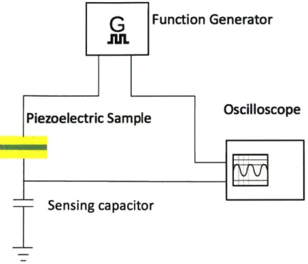
The Sawyer-Tower circuit75 is a classic configuration to obtain these quantities. In a typical setup, one uses a function generator to supply the sweeping voltage and a capacitor in series with the piezoelectric sample to measure the accumulated surface charge. An implementation using an oscilloscope is shown in Figure 3.1.2.
G
Function Generator
JUL
Piezoelectric Sample
Oscilloscope
Sensing capacitor
Figure 3.1.2 Sawyer-Tower circuit. In this configuration, the piezoelectric sample is in series with a capacitor of known value. The function generator supplies a sweeping voltage to the two capacitors, and to the x channel of an oscilloscope. The y channel of an oscilloscope is to measure the voltage across the sensing capacitor, from which the induced surface charge
can be calculated.
Since the sensing capacitor, whose value is known and denoted as Cs, is in series with
the piezoelectric capacitor C,, they share the same charge at any given point in time. By
measuring the voltage across the sensing capacitor, one can find the charge accumulated
on Cs from the relation Qs = V * Cs, and thus obtain Q,.
The polarization is then Q. divided by the area of the electrode. The sweeping voltage is given by the function generator setting, and can be converted to electric field strength easily.
Tek J SAVE/REC Action File Format About Saving Images Select Folder Save C NTEK0014.JPG
CHi 2.OOVEW
012
SOOmV*XY Mode
Figure 3.1.3
PE loop using an oscilloscope and a function generator. Sensing capacitance is 1 OuF, and the sweeping voltage is 1 OVpp at 400Hz.
However, due to the susceptibility to noise, the conversion from voltage to charge is prone to error, therefore this method is mainly used as a fast and qualitative measure.
In an alternative configuration, a varying voltage is applied through the electrodes across
the thickness of thin film, and the current flowing through the two electrodes is recorded.
As mentioned above, the sweeping voltage can be converted to electric field strength through division by sample thickness. Neglecting the leakage current, the measured current can be integrated to acquire the charge accumulated at the surface in an open-circuit setting. This derived charge, assuming uniform charge distribution across the area of the electrode, divided by the area, can give the average polarization density in the material. This second configuration is implemented using two pulse-measuring units
(PMU) on a Keithley 4200 semiconductor analyzer. A CV graph obtained in this method
is shown in Figure 3.1.3, which can be easily converted to a PE graph, shown in Figure
3.1.4.
Since the semiconductor analyzer can provide precise and accurate voltage and charge
CV Graph from PMU 3E-08 2E 1E-08 M -c -15 -10 -5 -1E-08 wj 4-$ 10 15 -2E-08 Force Potential(V) Figure 3.1.3
CV loop using Keithley 4200
Converted PE graph U300 U 0 0 40 30 100 -200 -1 0 100 200 300
Electrifc Field Strength (kV/cm)
Figure 3.1.4
PE graph converted from the CV graph
3.2 Voltage-Displacement Test
An alternative measure is to use a laser vibrometer to measure the vibration velocity of the piezoelectric elements under an external electric fields. This was done with the
equipment in Prof. Sang-Gook Kim's laboratory. Vibration velocity is measured through
interfering laser beams using doppler's effect. From this velocity, the average displacement of the piezoelectric units can be resolved, which is a measure of
deformation for a given driving voltage, and can qualitatively reflect the piezoelectric coefficients.
In the actual setup, a function generator is connected to the two leads of the actuator piezoelectric unit to induce vibration, and a laser beam with a diameter of about 1mm is aligned to the top surface of the actuator. By controlling the driving voltage amplitude, one can deduce the maximum out-of-plane displacement z from the relation:
z =- (4) f
where v is the measured velocity and f is the driving frequency. This displacement can be used as a qualitative reflection of electromechanical conversion.
Besides the actuator unit, this method can also be applied to the sensor for a quick examination of its integrity, in addition to PE sweep.
3.3 Actuator-Sensor Pair Response
In the complete measurement configuration, an AC driving voltage will be applied to the actuator unit, and a voltage readout will be connected to the sensor unit. According to the CMS and BN articles, the actuator-sensor units are sandwiched between a substrate and the target material whose mechanical properties are to be extracted.
This extraction relies on finding a correlation between the measured voltage output and the moduli of known materials, which was found to be a monotonic incremental relation in the two references respectively, and then extrapolating the acquired trend to obtain moduli of unknown materials.
The initial testing methodology is also to set up a similar measurement configuration and look at the trend of the sensor voltage output with respect to varying material moduli. The first configuration was to use a function generator to provide driving voltage to the actuator unit and measure the voltage output from the sensor unit using an oscilloscope,
and later with a digital volti-meter. This configuration was used in characterizing the first prototype design, which will be described in section 3.
A second configuration was to use a lock-in amplifier, as does in the two references. In
this configuration, a sine output voltage is supplied from an SR810 amplifier, and a differential voltage measurement is applied to the two electrodes connecting the sensing capacitor. This configuration was used in characterizing the second prototype design.
For the latest prototype design, whose testing will be beyond the timeline of this thesis, besides lock-in amplifier, more equipment will be used to characterize the sensor output
in order to find the best actuation and sensing parameters.
As will be discussed in Section 3, the cross-talk from the driving circuit coupled into the sensing circuit makes it difficult to determine the sensor voltage. For future experiment, a nanovoltimeter will be used to get an estimate of the sensor output, when a high frequency driving voltage is applied to the actuator. Additionally, a spectrum analyzer will be used to find out the frequency components of the AC voltage output from the sensor unit. Besides the previously mentioned harmonic driving voltage approach, a transient approach that applies a pulse signal to the actuator and measure the time delay in the sensor will also be explored. This is the method that follows the shear/surface wave dispersion vibrometry76,77method, which used phase velocity to extract tissue moduli.
4 DESIGN AND FABRICATION ITERATIONS
4.1 Design Overview
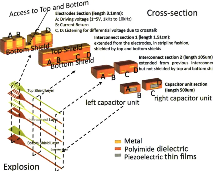
Within the timeline of this thesis work, the initial objective is to test a micro-fabricated front-end, and the design therefore does not include signal conditioning circuits that will be integrated in the final device. The initial design of the device consists of a pair of piezoelectric actuator and sensor, each with top and bottom electrodes to interface the external characterization equipment.
For insertion into tissue, a shaft with a higher stiffness is needed for penetration. In the initial design, a Kapton film (thickness 2mil or 3mil, 2.5GPa) is used as the substrate. The device is microfabricated on this film, which, after device fabrication, is patterned by
reactive ion etching to have a sharp tip to ease penetration.
This kapton film holder is later replaced by a borosilicate tube with a square cross-section (600pm-wide). A thin layer of uncured silicone is pasted onto of this tube, the microfabricated device is then laminated onto the silicone coating.
The initial designs did not take into account the effect of electromagnetic interference(EMI), which consist of two parts, contribution from the driving voltage, or cross-talk, and ambient electromagnetic noise. In the later designs, shielding layer is included to control the electromagnetic field in order to mitigate this effect. In this design, a bottom shield plate is first patterned on the substrate, the device with all the interconnects are patterned subsequently. Finally, a top shielding plate is patterned. The top and bottom shield plate are electrically connected at one of the device pinouts, so that they can be electrically grounded.
Due to magnitude of high EMI, and the low amplitude of the expected signal, FEM analysis is used to explore the relationship between the dimension of the capacitors and the expected output voltage. From these results, the dimension of the capacitors has also
4.2 Fabrication Process
This section will give a brief illustration of fabrication process flow of the core components of the device, which are shared by all designs.
The fabrication process flow begins with patterning the functional units, i.e. the piezoelectric actuator-sensor pair on the 1 st carrier wafer.
Starting with a wafer of silicon/silicon dioxide/titanium/platinum/PZT, a thin top electrode of chromium/gold is first deposited. Here, the gold is the major conductive material and chromium serves as an adhesion layer between gold and the PZT ceramics.
Alternatively, titanium can and will be chosen as the adhesion material for future experiment, as it can not only serve the same purpose as PZT, but also patternable with the etchant for PZT, which allows for full coverage of top electrode to the piezoelectric thin-films for better utilization of materials.
After the metal deposition, a 1um thick of positive photoresist AZ5214 is spin-coated on top, soft-baked, and then patterned into the top electrode geometry.
The two layers of metal are etched with commercially available etchant from Trancene, chrome etchant 1020 and Gold etchant type TFA, followed by removal of the AZ5214. Another layer AZ5214 of the same thickness is then spin-coated to covered both the top electrode and the exposed PZT and patterned in the same fashion into the geometry of the piezoelectric layer.
The etching of PZT is done with a solution of 49%Hydrofluoric (HF) Acid, Nitric Acid and de-ionized (DI) water in a ratio of 5:5:80. Since the HF etching of PZT usually generates water-insoluble fluoride that covers the PZT and interrupts the etching process, a specific rinse process is necessary for the etching to proceed. To remove the insoluble fluoride, immersion into a diluted Hydrochloric Acid (HCI) solution followed by DI rinse is done after partial etching of PZT. For the dimension of the samples and the 500nm PZT used in this work, 5s of immersion in the etchant, DI rinse, 5s of HCI solution, DI rinse, then another 3-5s of immersion in etchant is the adopted process.
After removing the AZ514, a 7um AZP 4620 is spin-coated and patterned into the geometry of the bottom electrode. After developing the PR with a diluted AZ 400K developer in a ratio of 1:2, the PR is baked at 110*C for over 40min to improve adhesion to the materials being protected.
Etching of the platinum bottom electrode is done with an aqua regia solution
(HCI:DI:HNO3 = 3:4:1), at a temperature of 850C, achieved through heating with a
hot-plate. In this step, the HCI will also remove the titanium layer underneath.
a
b
c
d
Figure 4.2.1
a) Deposit Au/Cr on top of the PZT wafer stack; b) Pattern Au/Cr as top electrodes; c) Pattern PZT; d) Pattern Pt/Ti as bottom electrodes
After the platinum etching, without removing the PR, the sample is immersed in HF solution for undercutting the SiO2, which serves as a sacrificial anchor layer. The purpose of undercutting is to remove SiO2 to a level where the capacitor stack is retrievable using an adhesive without mechanical damage or wrinkle.
ef
Figure 4.2.2
e) Wafer samnle before HF treatment: fHF undercut the sacrificial laver of SiO2.
been reported in the literature78. The key is controlling the adhesion between the pick-up
stamp and the top layer of the stacks and release rate of the stamp.
g
h
PDMS
1
s
Carrier Wafer
1 s
Carrier Wafer
2"d Carrier Wafer
Figure 4.2.3g) Apply PDMS to source wafer; h) Release PDMS with capacitors; i) Print capacitors to target
wafer
Gold/Chrome SiO2
PZT Silicon
Platinum/Titanium PI
Using an adhesive stamp made of poly-dimethysiloxane(PDMS) with a mixing ratio of base to cross-linker 8.5:1.5, the capacitor stacks are picked up from the 1st carrier wafer.
A target substrate is prepared separately for the printing stage. Earlier design used a
Kapton film as the target substrate. This was later replaced by a silicon wafer (2nd carrier
wafer) coated by 1 00nm of poly(methyl methacrylate) (PMMA) and 1.4[im of polyimide(PI). Prior to the printing stage, a 1.4pm of PI is spin-coated and soft-baked for 25s at a 11 0*C hotplate. The PDMS stamp with the capacitor facing down is pressed gently to the PI coated target substrate. This sandwich of PDMS-capacitor-substrate is then placed back to the 1 100C hotplate. After about 1min of heating, the PDMS stamp is release slowly,
and the capacitors are stuck to the target substrate by the Pl. A PI curing process of at least 1 h is required to cure the polymer.
A second layer of PI is then spin-coated and cured as an insulation layer, covering the
transfer-printed capacitor stacks. Using AZP 4620 as a masking layer, vias on the
insulating PI are opened through reactive ion etching(RIE) for interconnect traces to reach
chromium and gold, which is patterned into interconnect traces for accessing the capacitors.
i
k
Figure 4.2.4
j)
PI coating over the transfer-printed structure; k) Open vias to electrode through RIE;I)Deposition of metal as interconnect
Another layer of PI is spin-coated and patterned through RIE, serving as the final encapsulation while allowing for connection to external characterization electronics. As this thin-film device will be integrated with an insertion shaft, it needs to be yet again transfer from the silicon wafer. In the case of using a Si/PMMA/PI wafer, the PMMA serves the same role as SiO2, as a sacrificial anchoring layer and needs to be removed for successful device retrieval. This is done in by immersing the wafer and device in acetone heated to 750C. After enough undercut of the PMMA, the device is then pick-up with a
water soluble tape, made of either cellulose or poly vinyl alcohol.
A flexible ribbon cable, made of a thin layer of polyethylene terephthalate(PET) with silver
ink traces, is used to connect the device to an adaptor PCB to which BNC cables can connect.
4.3.1 DESIGN 01 (D1)
4.3.1.1 Design and Fabrication
A schematic of the first design is given below:
3.5mm A -L -/... . 4 I II 1 Au/Cr I PZT Kapton
Figure 4.3.1.1 D1. The dimension of the actuator (left, Au/Cr top electrode: 940pmx140ptm, piezoelectric layer: 1000pmx200pm, Pt/Ti bottom electrode: 1300pnx260tm) and the sensor (right, Au/Cr top electrode: 460imx80pm, piezoelectric layer: 500tpmx12Otpm, Pt/Ti bottom electrode: 660pnx180pm) units are similar to the ones in CMS, with a spacing between the edge of piezoelectric layer being 300pm. The width of the Kapton shaft is 3.5mm, with a length of 3.6cm.
As no discussion was given concerning the choice of dimension for the actuator and sensor units in the CMS, this design used similar dimensions for the piezoelectric actuator-sensor pair.
Micrographs of the fabrication process is shown as below:
a
300Im
Figure 4.3.1.2
a)PR pattern for gold- b)Gold etched; c)Chrome etched:d)Gold PR removed:
ef 300pm 9 - -4--Figure 4.3.1.3 -j b d
h 300pm
jhL
1
0 Figure 4.3.1.4h)PR pattern for platinum; i) PR hardbaked;
j)
Pt etched;k
300sm
Figure 4.3.1.5
k)Undercut of SiO2, followed by 1) removal of PR in acetone. The capacitor pair is now ready for release.
Figure 4.3.1.6
m) Capacitor pair picked up with PDMS stamp; n) Capacitor pair printed to PI coated Kapton substrate
Figure 4.3.1.7
I a, 300pm S U
I
Figure 4.3.1.8r)E-beam evaporation of Au/Cr for interconnect; s) PR patterned for Au/Cr; t) Au/Cr etching with chemical etchant; u)removal of PR with acetone
Figure 4.3.1.9
v)PR pattern for encapsulation PI; w) RIE etching of encapsulation PI; x) PR patterned for Kapton Etching; y)RIE etching of Kapton and removal of PR
4.3.1.2 Testing and discussion
After final patterning of the Kapton substrate, the fabrication process is complete. The Kapton is then released from the substrate. Heat seal connection ribbon cables are then bonded to the electrodes of the device and the tin traces on an adaptor PCB board.
a)
b)
it
11 iNw1
Figure 4.3.1.10
a) Dl transfer-printed to a silicone substrate; b) Dl connected to an adaptor two-layer PCB board, which is then connected to characterization equipment through BNC cables
A function generator () and an oscilloscope were connected to the pins on the PCB that corresponds to the actuator and sensor respectively. To remove the power line noise, a passive 100Hz high-pass filter is made using through-hole resistors and capacitors on a bread board and connected between the DMM and the sensor output pins on the PCB.
When the driving voltage is applied, a waveform with the same frequency can be seen on the oscilloscope. It was expected that putting a PDMS block onto the tip of the device would change the magnitude of this waveform. However, no significant change was observed on the scope screen.
To get a clearer picture of the problem, the oscilloscope was replaced with a digital voltimeter, using AC coupling. No difference in amplitude of measured voltage was observed when a PDMS block is placed onto the tip either.
Without the PDMS block, the measured amplitude increased with the driving frequency. Although this is consistent with the trend reported in the CMS article, that the amplitude
did not change with application of a PDMS stamps suggested that either this design is not effective or the measurement configuration is not precise enough.
Device 5V Frequency Response (Sensor Top Out) mV vs
kHz 1.8 1.6 1.4 1.2 0 1 0.8 0.6 0.4 0.2 0 0 10 20 30 40 50 60 70 80 90
Furthermore, in this adjacent interconnects structure, where the driving voltage circuit is 300-460pm away from the sensing circuit, a voltage difference between the sensing circuit interconnects can be induced by the driving voltage through electromagnetic coupling. This means that the actual measured voltage between the sensor electrodes Vmhas two components, one from piezoelectric thin film due to mechanical vibration, Vmech,
the change of which is the signal, the other is due to electromagnetic coupling, Vem:
Vm = Vmech + Vem (5)
The electromagnetic coupling between adjacent metal traces, or cross-talk(XT), is an important subject in radio-frequency circuit design. While the driving frequency used in this study falls into the low-frequency spectrum, the general characteristics of cross-talk include a positive correlation of the XT voltage in the victim circuit with the aggressor voltage frequency. This means that Vem in the sensor circuit should increase with an increasing driving voltage, which is also consistent with the trend in the frequency response shown above. Therefore, the frequency response may not be a pure reflection
There were several factors that could have affected the performance of this design.
1. Assuming the actuator piezoelectric units were functioning properly. If one is to adopt
the theory in the original CMS article, where adhesion and perfect contact is required for the fracture mechanics model to be valid, adhesion between the PDMS and the substrate
Kapton might be poor, which was limited by the pointy geometry at the tip.
2. For the layer structure of the capacitors, as shown in the schematic below, the encapsulation on the top and at the bottom of the capacitor stacks are effectively symmetric, considering the thicknesses of both the top and bottom electrodes (100 bottom/200nm top) are small compared to that of the encapsulating PI (1.4pm). And when properly functioning, the vibration should go through both the substrate material and the target material. As a result, the measured signal should be attributed to both, rather than just the target material.
The CMS article actually relied on the assumed condition of non-symmetric encapsulation, for the condition to be valid that the bottom encapsulation can shield the effect of the substrate, which was used to support the statement that what the CMS measured is solely attributed to the target material. However, this assumption is contrary to the actual layer structure of the CMS, as PI fully encapsulated the capacitor stacks.
On the other hand, this dependence of measured signal on both the substrate and target materials is reflected in the theoretical articles following the original CMS article6 8, shown as a function of Young's moduli in both the substrate and target, and also in the empirical scaling law presented in the BN article.
Following this dependence, while it can be argued that, changing the target materials and keeping all other parameters identical should theoretically cause some voltage output variation whose cause can be singly determined, practical measurement of this change is subject to sensitivity limitations, both in mechanism of how vibration is propagated and in the limitation on the measurement equipment.
Considering the case of the CMS, for most of the data points, PDMS(MPa) is in general much stiffer than the ecoflex substrate(80kPa), and the CMS appears to be more sensitive to the stiffer of the two. If this trend is true for D1, which shares similar geometry, then the stiffness of the Kapton substrate(GPa) may have caused the device to be non-sensitive to anything softer than the Kapton.
b
a
C Au/Cr * PZT P1/Ti Kapton Figure 4.3.1.11a)Thin film stack with realistic scale for the thickness of each layer. The PI coating is effectively symmetric to PZT layer; b)Device on Kapton substrate; c) Device with Kapton substrate in contact with soft material. Both the Kapton and the soft material transmit the
vibration and contribute to the sensor deformation.
3. No discussion was given in either the CMS or the BN article concerning the possible
electromagnetic interference. In both cases, the interconnects or electrodes for the actuator and sensor have sections that are 300pm away from one another. The AC driving voltage supplied to the actuator can couple either capacitively or inductively into the sensor measuring circuit. This coupling is even more severe in D1, since the interconnects are almost 4cm long and in parallel. If this contribution from the driving
4. It was not found until the fabrication of the second design, when the Keitheley semiconductor analyzer was available, that high temperature (up to 3000C) significantly
affects the polarizability of the piezoelectric thin films. Since the fabrication process in D1 used 350'C to cure the insulation polyimide polymer, this could have deteriorated the piezoelectric material.
To determine whether electromagnetic crosstalk actually exist, mock samples without any piezoelectric units and interconnects of the same length were fabricated and tested with the same measurement configuration. The frequency response for the measurement
nodes are shown in the figure below,
Mock Device 5V Frequency Response (Sensor Top Out) mV vs kHz 3.5 E kn 3 0 2.5 CL) E 2 E 0 w 1.5 0 > 1 0.5 0__ 0 10 20 30 40 50 60 70 80 90
Driving Voltage Frequency (kHz)
As shown, increasing driving voltage frequency will lead to an increase in the measured
AC voltage amplitude between the sensor nodes.
Further, a comparison is drawn between the frequency response of a device with piezoelectric units and that of the same device with sensor tip (section where the piezoelectric units are located) removed. The result is shown as below:
3.5 3 - 2.5 E 2 0 1.5 0.5 0 0.00E+00
Device Frequency Response, 10V input, mVvs Hz
e0
1.00E+04 2.OOE+04 3.OOE+04 4.OOE+04 5.00E+04 6.OOE+04 7.OOE+04 8.OOE+04 9.OOE+04
Driving Voltage Frequency (Hz)
M Original Device 0 Device without piezo-units
The similar trends of these two graphs led the author to believe that the abovementioned electromagnetic crosstalk voltage does exist, and may have made major contribution to the measured voltage. The author therefore sought to improve this design by going through a second iteration.
4.3.2 DESIGN 02 (D2)
4.3.2.1 Design and Fabrication
To address the issues found in D1, particularly issue 2 and 3, and also to enable positioning the device onto the surface of a borosilicate tube with a width of 600 pm, the device was modified into D2.
Compared to D1, D2 has a pair of top and bottom shield plates covering the interconnect. These shield plates are grounded when the device are connected to the driving voltage.
The design of these shield plates went through several iterations as shown below, and the final design was chosen based on simulation results and fabrication consideration.
InDut Channel Shielded
Both Channels Shielded
Both Channels Shielded. seoaratelv
erounded
Figure 4.3.2.1 Cross-section view of initial designs of shielding layerThe initial design follows the principle of converting the original interconnects to a shield wire fashion, where the driving interconnects and the sensing interconnects are isolated
by top and bottom grounded shield plates, which are connected at the center.
A bottom shield plate is first patterned through lift-off after transfer-printing the capacitors. A 1.4pm PI is then deposited on the capacitors and the shield plate. A following RIE process then open the vias reaching the capacitors as well as a trough at the center, enabling access to the bottom plate. A central metal strip is patterned together with the interconnect. After patterning the 1.4pm encapsulating PI that follows, which allows access to the electrodes and the bottom shield plate, a top shield plate is patterned.
Fabrication of this design faced some yield issue due to the proximity of the central strip with the interconnect(10pm). The limited resolution of the photolithographic step and chemical wet etching of the interconnect layer (300nm Au/ 1 Onm Cr) has the probability to leave some residual between the strip and neighboring interconnect traces, which led to shorting of the shield plates and the driving/sensing circuits.