Gold Nanoparticles on Oxide-Free Silicon
−Molecule Interface for
Single Electron Transport
Louis Caillard,
†,‡Oliver Seitz,
†,∥Philip M. Campbell,
†Rachel P. Doherty,
‡,§Anne-Fe
́licie Lamic-Humblot,
§Emmanuelle Lacaze,
‡Yves J. Chabal,
†and Olivier Pluchery*
,‡†
Laboratory for Surface and Nanostructure Modi
fications, Department of Materials Science and Engineering, University of Texas at
Dallas, 800 West Campbell Road, Dallas, Texas 75080, United States
‡
Institut des NanoSciences de Paris, Universite
́ Pierre et Marie Curie UPMC-CNRS, 4 place Jussieu, 75005 Paris, France
§
Laboratoire de Re
́activité de Surfaces, Université Pierre et Marie Curie UPMC-CNRS, 3 rue Galilée, 94200 Ivry-sur-Seine, France
ABSTRACT:
Two di
fferent organic monolayers were prepared on
silicon Si(111) and modi
fied for attaching gold nanoparticles. The
molecules are covalently bound to silicon and form very ordered
monolayers sometimes improperly called self-assembled monolayers
(SAM). They are designed to be electrically insulating and to have very
few electrical interface states. By positioning the tip of an STM above a
nanoparticle, a double barrier tunnel junction (DBTJ) is created, and
Coulomb blockade is demonstrated at 40 K. This is the
first time
Coulomb blockade is observed with an organic monolayer on
oxide-free silicon. This work focuses on the fabrication and initial electrical
characterization of this double barrier tunnel junction. The organic
layers were prepared by thermal hydrosilylation of two di
fferent alkene
molecules with either a long carbon chain (C
11) or a shorter one (C
7),
and both were modi
fied to be amine-terminated. FTIR and XPS measurements confirm that the Si(111) substrate remains
unoxidized during the whole chemical process. Colloidal gold nanoparticles were prepared using two methods: either with citrate
molecules (Turkevich method) or with ascorbic acid as the surfactant. In both cases AFM and STM images show a
well-controlled deposition on the grafted organic monolayer. I
−V curves obtained by scanning tunneling spectroscopy (STS) are
presented on 8 nm diameter nanoparticles and exhibit the well-known Coulomb staircases at low temperature. The curves are
discussed as a function of the organic layer thickness and silicon substrate doping.
1. INTRODUCTION
Despite almost 40 years e
ffort and the opening of great routes
for future applications, molecular electronics is still in its
infancy. Indeed, it o
ffers an unprecedented way for controlling
the morphology at the subnanometer level based on its ability
to build functional organic layers on silicon substrates as
detailed in several recent reviews.
1,2A functional organic layer
should also be able to carry out electrical functions such as
driving charges with a high mobility, storing electrons in a
memory device,
3or controlling their
flow in a transistor.
4,5However, this requires a high degree of morphologic
organization close to what is achieved in a silicon crystal. If
not, the memory will leak and exhibit a poor retention time, the
electrons will be trapped,
6or the Fermi level will be pinned in a
noncontrollable way.
7Therefore, it is crucial to succeed in
assembling molecules on silicon with atomic precision, starting
with the most straightforward layer, an insulating layer.
In this article we describe a chemical route for building two
di
fferent organic monolayers grafted on silicon and acting as
ultrathin insulating layers. In order to probe the electrical
quality of the organic layer, gold nanoparticles (AuNP) from
colloidal solutions are covalently attached on top of the
monolayer. The whole process is achieved by wet chemistry. It
preserves an oxide-free silicon substrate that remains stable
under ambient conditions. This architecture serves as a
first
tunnel junction (silicon/organic layer/AuNP junction) and is
completed by a second tunnel junction established with an
STM tip (AuNP/vacuum/tip junction). Such a double barrier
tunnel junction (DBTJ) exhibits an electric behavior
charac-terized by Coulomb blockade which is detectable at 40 K in
UHV. This work focuses on the fabrication and initial electrical
characterization of this double barrier tunnel junction.
Coulomb blockade
is a typical single charge phenomenon
where electrons can be controlled one by one by adjusting the
potential applied to the DBTJ. It is based on the fact that the
system is mostly capacitive and the value of the capacitance is
roughly proportional to the nanoparticle diameter. The
electrostatic energy needed to add one more electron to the
nanoparticle (called the island) is expressed as e
2/2C, where e is
the unit charge and C the capacitance. For very small
nanoparticles this energy becomes larger than kT and the
electrostatic energy overcomes the thermal noise, so that the
electron
flux can be controlled by an external applied potential.
At room temperature, this condition is ful
filled for
nano-particles smaller than 5 nm. In the early 2000s, a strong interest
arose for single electron phenomena such as the Coulomb
blockade, fueled by the hope of creating new architectures for
single charge electronics.
8−11Some single electron transistors
have been fabricated
12−15as well as nonvolatile memories.
16,17However, the development of devices based on single electron
transport faces serious challenges due to the poor
reproduci-bility of these devices and the di
fficulty in precisely controlling
Coulomb blockade phenomena. One reason for this lies in the
insufficient control of the interface quality and the nanogap
thickness.
18In order to observe single electron phenomena, the
targeted device is the DBTJ. Given that the tunnel current
depends exponentially on the barrier thickness, an accurate
control of the samples geometry is necessary. Moreover, the
typical thickness of such junctions lies between 0.8 and 2 nm,
which requires that the tunnel barrier thickness must be
controlled at the atomic level. Such a control can best be
achieved with self-assembled monolayers.
Highly ordered monolayers on silicon
have been explored for
decades, particularly after the discovery of a process to form
atomically
flat hydrogen-terminated silicon surfaces in 1989.
19Starting from this H
−Si(111)-(1 × 1) surface, many chemical
routes
20have been used for replacing the terminal hydrogen by
other molecules: thermal activation
21−24UV activation,
24−27electrochemical activation,
28,29and chlorination.
24,30,31More
recently, some of these groups started investigating the
electrical quality of these organic layers in order to integrate
them within future functional architectures.
1,32The monolayer
is probed either globally, with the mercury drop method,
33,34with electrochemistry,
27by depositing an oxide layer
35or a
metallic electrode, or sometimes local probes such as KPFM or
conductive AFM are used.
26From these studies, it appears that
the Si
−organics interface can be made with a notably low
amount of surface defects, in line with expectations based on
the H
−Si(111) interface.
33,35,36Interestingly silicon surfaces
functionalized with organics are usually much more stable
against oxidation
6(e.g., up to 1 month) than H
−Si(111)
surfaces, which is encouraging for implementing a robust
functional molecular passivation of silicon surfaces.
2. EXPERIMENTAL METHODS
Preparation of Highly Ordered Monolayers on Si(111). Samples of 5× 12 mm2were cut from n-doped silicon (111) wafers with resistivity of either 0.03Ω·cm (∼1 × 1018cm−3) or 7Ω·cm (∼6 × 1014cm−3). Float zone (FZ) grown samples were chosen in order to minimize the amount of oxygen and allow an accurate monitoring of potential surface oxidation with FTIR.23,30,37It should be noted that the chemistry described here works equally well with Czochralski-grown wafers but depends on the level of doping.26Functional organic monolayers were prepared within four steps (see Scheme 1). In step 1, samples were initially cleaned in a piranha solution at 80 °C (3:1 H2SO4 98%: H2O2 30%) and copiously rinsed with ultrapure water (18 Mohm·cm, Millipore). Atomically flat, hydrogen-terminated Si(111)-(1 × 1) surfaces were prepared by oxide removal in a concentrated HF solution for 30 s, followed by a 150 s immersion in 40% NH4F solution and thorough rinsing in deionized water.19,26,38 Caution is recommended because the piranha solution reacts strongly with organics, and the HF solution is extremely harmf ul. Both solutions should be handled with due protection: goggles and suitable gloves. Starting from a set of two different hydrogen-terminated Si(111)-(1 × 1) surfaces, step 2 consists of covalently attaching the organic layer by direct thermal hydrosilylation with either a long alkyl chain of 11 carbon
atoms (Si−C11samples) or a shorter chain with 7 carbon atoms (Si− C7samples).
Si−C11. 10-Carboxydecyl organic monolayers were grafted on the hydrogenated silicon via direct thermal hydrosilylation of ethyl undecylenate. The neat alkene was outgassed three times by freezing it using liquid nitrogen under low vacuum (10−2Torr) in a Schlenk tube. It was then heated up to 200 °C under continuous argon bubbling when inserting the freshly prepared H-terminated silicon sample. Grafting was performed for 4 h.
Si−C7. 6-Carboxydecyl organic monolayers were grafted on the hydrogenated silicon via direct thermal hydrosilylation of ethyl 6-heptenoate diluted (1:1) in mesitylene following the same procedure described above. Notable differences are the use of a lower vacuum during the outgassing step (10 Torr) with liquid N2, and thermal hydrosilylation is performed at 170°C. Both modifications are done to avoid evaporation of the molecule and most of the solvent during the preparation and the reaction. At the end of this second step both organic monolayers are terminated with a protected carboxylic acid.
In step 3, the functionalized surfaces were sonicated in ethyl acetate and rinsed in boiling dichloromethane (40°C). The carboxylic acids groups were then deprotected by using potassium tert-butoxide in DMSO (for 90 s and then rinsed thoroughly with DMSO) and by finally using an acid solution (HCl) to protonate the active group. Finally, step 4 is the transformation of the functional headgroup into succinimidyl ester-terminated. This was performed by reaction with an aqueous solution of N-ethyl-N′-(3-(dimethylamino)propyl)-carbodiimide (EDC). After a few minutes in EDC solution, 1 mL of ethylenediamine is added to the solution for 1 h 30 min at room temperature. Finally, the surface was rinsed with ultrapure water. During the last step, one amine group of the ethylenediamine molecule (H2N−CH2−CH2−NH2) reacts with the activated ester, leading to the attachment of the molecule via an amide bond (−(C O)−NH−CH2−CH2−NH2). It is very unlikely that the ethylenedi-amine binds in a bridging configuration through its two ethylenedi-amine ends because the molecule length (2.99 Å) is shorter than the typical distance between two COOH groups estimated from the Si−Si distance. Therefore, at the end of step 4, the resulting surface presents amine groups on top of the layer.36,39,40
FTIR Characterization of the Grafted Organic Monolayers. All FTIR spectra were taken using a Nicolet 6700 FTIR spectrometer from Thermo Scientific equipped with a DTGS detector in transmission mode at an angle of incidence of 64° with respect to the Si surface normal in a dry N2(g)-purged atmosphere and with an unpolarized IR beam. The spectra were obtained after the initial
Scheme 1. The Four Steps for Preparing the Two Kinds of
the Grafted Organic Monolayer Considered in This Study
molecular attachment and deprotection of the carboxylic acid, i.e., after step 3. The reference spectra were recorded in both cases using the oxide-free, fully hydrogen-terminated Si(111) surfaces.
In the case of Si−C11, no oxide was detected. This surface remains robust against oxidation as evidenced by the absence of any detectable absorption at 1080 and 1240 cm−1(TO and LO modes of SiO2oxide) in Figure 1. In the case of Si−C7a negligible amount of oxide shows
up at 1080 cm−1. This oxide uptake is due to the time spent by the sample in air, needed for recording the FTIR spectra, and this characterization step was discarded for the samples used for STM measures. The negative peak at 2093 cm−1is due to the replacement of Si−H bonds with Si−C bonds in the hydrosilylation process. Knowing that a fully hydrogen-terminated Si surface exhibits a Si−H line with an area of 0.08 cm−1, an area comparison between the Si−H peak before and after molecular grafting shows that a coverage of roughly 1/2 of the surface is obtained for the SiC11and slightly more for the SiC7. Half of the hydrogen atoms remains on the unreacted silicon atoms as depicted in Scheme 1. The peak at 1713 cm−1 is assigned to the terminal CO bond. The two peaks at 1280 and 1410 cm−1 correspond to the C−O bonds, and the 1461 cm−1 band is due to the bending mode of the methylene groups of the alkyl chains. The positive peaks in the range of 2880 and 2920 cm−1are due to the CH2 chains. They exhibit a higher area in the case of Si−C11, confirming the presence of a longer chain.
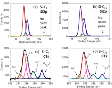
XPS Characterization of the Grafted Organic Monolayer. Surface analysis after molecular grafting using X-ray photoelectron spectroscopy after step 2 confirms that there is no oxide present (see Figure 2) and gave almost identical results for both monolayers: in the vicinity of Si 2p core level shift, there is no evidence of Si oxidation (i.e., at 103.2 eV). Moreover, the C 1s region shows the specific peaks corresponding to the ester (290.0 eV), the C−O bond (288.0 eV), the C−C bond (285.0 eV), and the Si−C bond (284.5 eV). This last peak is less intense than the C−O and the ester peaks because it corresponds to carbon located deeper in the sample; i.e., fewer photoelectrons can escape. An additional peak is also observed at 286 eV and is attributed to organic contamination because of exposure to air after surface chemistry during transport to the XPS chamber.
Spectroscopic ellipsometry measurements were also performed on the samples before gold nanoparticle deposition using an HORIBA Jobin Yvon ellipsometer (iHR320). After organic modification, the thickness and the dielectric constant of each organic layer are determined using a simple two-layer model similarly to our previous study.23The thicknesses of the layers derived from the results are 1.6 nm for the Si−C11 and 1.3 nm for the Si−C7. These results are in agreement with the expected values (1.67 and 1.28 nm, respectively) calculated from the geometry of the molecules.
After monolayer preparation and initial characterization, the samples were express shipped inside an argon-filled plastic container
from Dallas to Paris. The samples were stored under vacuum at a pressure of 10−8Torr as soon as they were received. The surfaces were subsequently further functionalized by gold nanoparticles and then characterized with UHV STM. It is important to stress that the samples remain stable in air for several days, before notable oxidation of the Si−C11surface is observed. We checked that STM was able to image straightforwardly the surface as long as it is not kept in air for too long a time. Typically after 2 weeks in air, STM imaging is no longer possible because silicon oxide has regrown underneath the organic layers with a thicknesses greater than ca. 0.6 nm, an oxide thickness preventing proper STM under normal conditions.41 This stability against silicon oxidation of these grafted organic monolayers is one of their main interests.
Gold Nanoparticle Preparation and Deposition. Two different methods were used to prepare colloidal gold nanoparticles (AuNP):
1. Turkevich AuNP. The citrate reduction method for synthesizing gold nanoparticles in water was pioneered by Turkevich et al. in 195142and modified by Frens in 1973.43It remains one of the most popular methods for producing spherical monodisperse gold nano-particles. An aqueous solution of HAuCl4 (20 mL, 0.25 mM) was boiled under refluxing conditions and vigorous stirring. Sodium citrate was quickly added (1 mL, 18 mM), and the solution color changed from faintly yellowish to clear gray, purple, and finally dark purple within 2−3 min. The resulting AuNP have a diameter of typically 15 nm as already established44−46and demonstrated below by AFM. In this reaction, citratefirst acts as a reducing agent and tends to adsorb onto the metallic gold clusters, slowing down their growth and resulting in size regulation. Moreover, citrate ions are negatively charged such that the nanoparticles repel each other.45,47,48
2. Ascorbic Acid Nanoparticles (asc-AuNP). The asc-AuNP were synthesized following a method described elsewhere.49Typically, 200 μL of an aqueous solution of HAuCl4·3H2O (10 g L−1of gold) was added to 25 mL of water at around 2°C (ice-cooled) in a beaker. Then, 1.5 mL of a Na2CO3solution (21.2 g L−1) and 1 mL of an ascorbic acid solution (7 g L−1) were added under vigorous stirring. The solution became instantaneously dark red.
Deposition of AuNP on the organic monolayer was performed by dipping the functionalized silicon substrate into the colloidal solutions. The attachment occurs through the interaction between the −NH2 moiety of the organic layer and gold surface. In the case of Turkevich AuNP the maximum nanoparticle coverage is reached after 1 h and occurs with an initial step of electrostatic attraction between the negatively charged citrate and the −NH3+ end group which is protonated due to the acidity of the Turkevich solution (pH = 5). In Figure 1.FTIR transmission spectra showing the organic monolayer
fabrication when the surface is terminated with carboxylic acid at step 3 (see Scheme 1). The monolayer was obtained by thermal hydrosilylation with ethyl undecylenate (abbreviated Si−C11, spectrum a) and ethyl 6-heptenoate (Si−C7, spectrum b). The reference spectra were recorded in both cases using the oxide-free, fully hydrogenated Si(111)-(1 × 1) surface. These spectra demonstrate that the hydrosilylation process occurs without oxidizing the silicon substrate.
Figure 2.XPS characterization of Si−C11and Si−C7molecules after thermal hydrosilylation. The C 1s peaks between 284.5 and 290.0 eV observed for both Si−C7 (a) and Si−C11 (b) confirm that the molecules are grafted on the surface. The Si 2p regions for Si−C7(c) and Si−C11(d) contain no evidence of oxidation.
the case of the asc-AuNP, the solution wasfirst acidified to pH = 6 with a 0.1 M hydrochloric acid solution. The solution color remained unchanged. The functionalized silicon surface was dipped into the AuNP solutions for 12 min, allowing the particles to become grafted onto the amino-terminated surface while remaining well separated. In both cases, the substrate was cleaned after the dipping by several rinses in deionized water and dried with a nitrogen gas stream.
AFM Characterization of AuNP on the Monolayer. AFM was performed on these surfaces using the tapping mode with a Digital Instrument DI-3000 (Figure 3a) or a Multimode-8 instrument from Veeco (Figure 3b) and were processed with the software WSxM.50
In the case of the Turkevich AuNP, the deposition was carried out as a test experiment to make sure that attachment occurred on the oxide-free monolayer investigated here similarly to what had been previously demonstrated in other publications dealing with monolayer on oxidized silanized silicon surfaces.44,46,51 The amino-terminated monolayer layer was confirmed as being very efficient at immobilizing the nanoparticles,23 and the AFM images acquired in tapping mode showed no indication that the AuNP were moved by the tip. However, Turkevich nanoparticles are too large (diameter ∼15 nm) to exhibit Coulomb blockade at room temperature since this phenomenon requires NPs diameter around 5 nm. Therefore, we concentrate on the asc-AuNP. As shown in Figure 3b, the asc-AuNP are randomly distributed over the organic layer and there was no aggregation. Based on their profile height, the average size of the nanoparticles is 9.5 nm (standard deviation of 2.5 nm). Practically, this means that it is possible tofind nanoparticles with a diameter between 4 and 15 nm on a typical AFM or STM image. The roughness of the underlying substrate without nanoparticles was measured to be 0.36 nm.
STM. STM images were recorded with a commercial apparatus (Omicron VT-STM) whose UHV chamber has a base pressure of 4× 10⁻¹¹Torr, in which the sample could be cooled down to 25 K with a coldfinger in contact with liquid helium. The samples were introduced into the preparation chamber with a load-lock and then annealed at 150 °C for 30 min before STM imaging. This annealing procedure removes any physisorbed water molecules and greatly improves the image quality by minimizing fuzzy structures during imaging. The organic layer is not affected by this thermal treatment because it was prepared at similar temperatures. Imaging a given sample before and after annealing (though not on the same area) allowed verification that the AuNP distribution did not change significantly before and after this annealing procedure. In the STM experiments, the indicated voltage is the bias of the surface relative to the tip.
3. RESULTS AND DISCUSSION
STM Characterization. STM images of the two kinds of
organic-functionalized surfaces (see Scheme 1) were recorded
in UHV at room temperature prior to AuNP deposition, as
shown in Figures 4a and 4b. The surfaces are remarkably
flat
with a rms roughness of 0.33 and 0.38 nm, respectively, in
agreement with AFM experiments, which indicates that the
monolayer is very well ordered. The surface shown in Figure 4a
exhibits parallel lines that are attributed to the silicon terraces.
26The inset in Figure 4b shows that 3 nm large protrusions can be
resolved, corresponding to bundles of
∼10 molecules.
52STM
imaging found no notable di
fferences between Si−C
7and Si
−
C
11surfaces.
After the asc-AuNP were grafted ex situ as described above,
the samples were analyzed again by STM. As evidenced in
Figures 4c and 4d, AuNP are clearly visible, with a topographic
distribution comparable to what was measured by AFM (Figure
3). The AuNP were strongly attached and could not been
displaced by the STM tip as might occur on other systems such
as self-assembled monolayer on Au(111). The diameters of two
particles (marked with a cross in Figures 4c and 4d) were
evaluated, taking advantage of their height and found to be 7.5
nm for both particles.
STS Measurement. After acquiring an STM image, the
current
−voltage spectra I(V) were recorded on various AuNP
selected on the basis of their size (closest to 5 nm) and having
su
fficient separation from neighboring particles. The tip was
placed above each AuNP at a distance determined by the
current set point used for imaging, typically between 20 and 50
pA. At ca. 40 K, the typical lateral drift was 0.4 nm/min after 1
h stabilization time. For each image and before I(V) acquisition,
this drift was precisely calculated, and a correction was applied
so that the tip did not move more than 0.01 nm over a
nanoparticle during data acquisition. After having switched o
ff
the feedback loop, a series of 40 spectra were acquired and
Figure 3.AFM images in tapping mode of AuNP deposited on highly ordered monolayers on Si(111)-(1 × 1) surfaces. The Turkevich nanoparticles (a, c) were deposited on the Si−C11organic layer and the asc-AuNP (b, d) on a Si−C7organic layer.
Figure 4. STM images (100 × 100 nm2) of different surfaces of organic layers grafted with a Si−C bond to the Si(111) substrate. Surfaces (a) and (c) were prepared with the long chain molecule (Si− C11) and surfaces (b) and (d) with the shorter chain (Si−C7). Inset in image (b) is a 20 × 20 nm2zoom of the surface with an enhanced contrast showing the molecular bundles on the surface. On both surfaces, asc-AuNP have been grafted through the −NH2 terminal group of the organic monolayer (images c and d). The cross indicates the AuNP where STS was performed. Images (a) and (b) have been recorded at room temperature and images (c) and (d) at low temperatures (25 and 37 K, respectively). Scanning conditions are given on the images (gap voltage and current set point).
averaged. However, a few curves were usually dropped from the
averages because of tip mechanical instability. As depicted in
Scheme 2, positioning the STM tip over a gold nanoparticle
creates a double barrier tunnel junction (DBTJ). The
first
barrier is composed of the organic layer and the second of the
vacuum gap between the tip and the nanoparticle. This system
can be electrically modeled by the circuit represented in
Scheme 2 where each tunnel junction is represented by a
capacitance and a resistance in parallel. If the two junctions are
symmetric, the I = f(V) curve exhibits a Coulomb blockade
region (
−e/2C < V < e/2C) where no current flows through the
DBTJ, and an Ohmic behavior is expected outside this region.
On the other hand, if the DBTJ is asymmetric, the I = f(V)
curve is staircase-like, and the number of extra electrons
simultaneously present in the island is a discrete number
directly controlled by V.
53About 100 AuNP were investigated
under di
fferent conditions: three different temperature ranges
(room temperature, 100 K with liquid nitrogen, and 25
−40 K
with liquid helium cooling), two di
fferent monolayer
thicknesses (C
7and C
11), two di
fferent substrate doping, and
several AuNP diameters ranging from 4 to 10 nm. In this paper,
we select a few examples to illustrate the performance of this
organic monolayer-based system, and we restrict ourselves to
nanoparticles of one size.
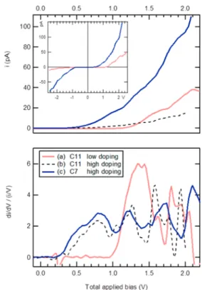
Coulomb Blockade. I(V) spectra on three AuNP of similar
size (8 nm) are presented in Figure 5: two spectra were
recorded with the same Si
−C
11monolayer, but with two
di
fferent substrate doping levels, and the third spectrum was
taken on the thinner Si
−C
7layer. They illustrate the
understanding of the in
fluence of the thickness of the tunnel
barrier and the in
fluence of the semiconductor doping level on
electron transport. The spectra were recorded at low
temperatures (25, 37, and 100 K, respectively). In all three
samples, Coulomb staircases were observed (top graph of
Figure 5) and are evidenced by di
fferentiating the i(V)
spectrum and calculating (di/dV)/(i/V). The quantity di/dV
is proportional to the local density of states (LDOS) and allows
detecting the electrostatic energy levels generated by Coulomb
blockade in the metallic island.
11Each Coulomb oscillation in
the di
fferentiated curve corresponds to a step of the Coulomb
staircase, indicative of an additional electron stored in the
nanoparticle. These results demonstrate that the quality of an
organic monolayer on silicon can be such that they act as a local
tunnel barrier between the substrate and a metallic nanoparticle
and that it is possible to prevent an insulating oxide from being
spontaneously formed. However, the exact Coulomb blockade
behavior depends on many parameters such as the size and
shape of nanoparticles, their crystallinity,
54the presence of an
organic surfactant on the nanoparticle, and the actual bonding
between the nanoparticle and the organic layer. These delicate
issues have barely been investigated in the literature so far, and
we do not address them in detail in the present article. A
further analysis of our acquired data set will be reported in a
forthcoming article and will focus on the transport
measure-ments in a more quantitative approach. Nevertheless, we
checked that on the three nanoparticles discussed herein
Coulomb blockade was repeatedly observed during a
measure-ment campaign and that for a given particle the positions of the
di/dV peaks were reproduced within an interval of 0.08 V.
In the case of the low doped substrate (N
d= 6
× 10
14cm
−3)
and with the Si
−C
11layer (curve a in Figure 5), the current
onset is measured at V
0= 1.37 V, and the second step shows up
at V
1= 1.87 V (see Table 1 for an overview of the relevant
experimental values). According to the theory developed for
Coulomb phenomena on metals,
10,53the step position is given
by V
n= (2n + 1)e
2/2C: the current onset is expected at a
potential that is the half of the step width. Obviously this is not
the case in the present experiments since V
0≠ 1/2(V
1− V
0). In
order to understand the reason for this apparent discrepancy,
the doping of the substrate was increased to N
d= 7
× 10
17cm
−3, keeping the same molecular insulating layer and the same
nanoparticle diameter. In this case the current onset was
lowered to V
0= 0.85 V, and the
first step is measured at V
1=
1.22 V (curve b in Figure 5). The di
fference between the
measured and theoretical onset is due to the strong band
bending e
ffect occurring in silicon substrates and particularly in
those that are low doped. These e
ffects are qualitatively shown
Scheme 2. Configuration Used To Build a Double Barrier
Tunnel Junction with the Tip of the STM Placed above a
Nanoparticle
Figure 5. Tunnel spectroscopy on 8 nm nanoparticles at low temperatures (25, 100, and 37 K, respectively) showing Coulomb staircases (upper graph) and its derivative (di/dV)/(i/V) (lower graph). Each peak of the derivative corresponds to a supplemental electron added to the nanoparticles. Spectra (a) and (c) were recorded on the AuNP marked with a cross in Figures 4c and 4d, respectively. The silicon substrates were n-doped in all cases with a carrier density of 4× 1014cm−3, 7× 1017cm−3, and 2× 1018cm−3, respectively.
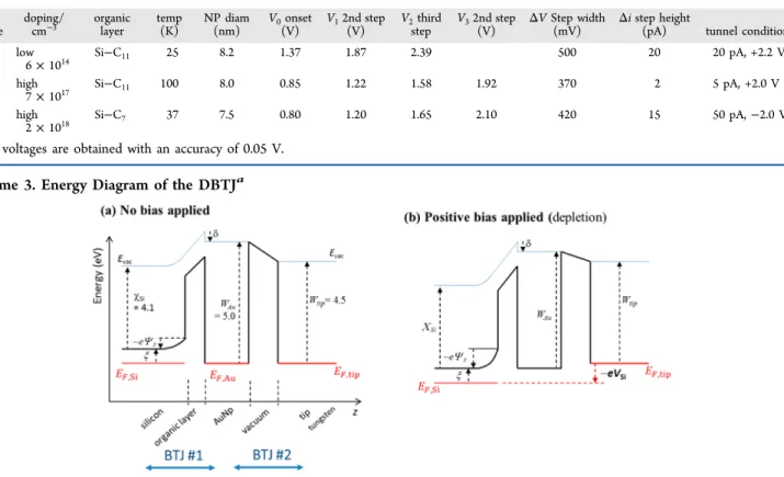
in Scheme 3 where the energy pro
file is drawn as a function of
the distance away from the silicon surface. This scheme clearly
shows the two barriers that an electron needs to cross in order
to travel from the substrate to the STM tip. In the present case,
both barriers are of the order of 1 nm and an electron can
tunnel through them. The pro
file is derived from the work
functions of all the materials of the DBTJ, knowing that the
Fermi levels should be aligned through the entire structure
when no bias is applied.
55,56For the
first barrier tunnel junction
(denoted BTJ
#1), the work function of silicon W
Siis given by
the sum of the electron a
ffinity of silicon χ
Siand the energy
di
fference ξ = E
C− E
F,Sisuch that W
Si=
χ
Si+
ξ ≈ 4.4 eV. χ
Siis
slightly attenuated by the electrostatic dipole generated by the
molecular layer. The molecular dipole
δ is independent of the
applied bias and was evaluated at around
−0.4 V in similar
cases.
22,57In Scheme 3 this dipole shows up as shift of the
vacuum level indicative of an electric
field close to the organic
surface. The Fermi levels of silicon and gold are aligned at
equilibrium, and since the work function of gold is W
Au= 5.0
eV, it results in the creation of an electric
field between the two
materials so that the bands of the semiconductor tend to bend
upward even at zero applied bias. As a consequence of this band
bending, an interface potential is generated, denoted
Ψ
Sin
Scheme 3. When a positive bias V
Siis applied as depicted in
case b of Scheme 3, the band bending is ampli
fied and the
electron needs to roll up this supplemental hill to reach the tip.
As a result, a supplemental amount of energy needs to be
provided, which is done by further increasing the applied
voltage V
Si. This e
ffect is all the more important when the
doping is low. This explains why the steps of the Coulomb
staircases were detected at higher potential for the low doped
samples. Therefore, band bending has two consequences:
first,
the actual interface potential applied to the silicon/organic
layer/AuNP system is much weaker than the external potential
applied by the STM tip, and the electrons need to climb this
supplemental barrier. Second, the process depends on the
thickness of this barrier, which can be very thin in the case of
high doping allowing the charges to tunnel through it. This is
not the case for low doped substrates due to band bending. The
band bending potential at zero bias has been evaluated to be
+0.60 V for low n-doped substrate (10
15cm
−3) and +0.50 V for
highly n-doped silicon (10
19cm
−3) by Cahen
’s group.
58Hacker
found a value of +0.26 V with low n-doped substrate (4
× 10
14cm
−3).
22Although these two values di
ffer, probably because of
the di
fferent ways of estimating the molecular interface dipole,
they con
firm the order of magnitude of the voltage shift
observed in our experiments.
Finally, with the shorter Si
−C
7monolayer, the Coulomb
phenomena are even more pronounced, as shown in curve c of
Figure 5: the steps are clearly visible, and the current is stronger
due to a higher conductance of this thinner organic layer. The
current onset is detected at 0.80 V, very similar to curve b,
because the doping level and nanoparticle diameters are
identical. The step widths are also comparable. It is not
possible to compare the step height since the tunneling
conditions were not the same for these three experiments (see
last column of Table 1), and the actual tip
−nanoparticle
distances di
ffer and are unknown in all three cases.
The inset in Figure 5 illustrates another consequence of
working with a low doped substrate. With the high doped
substrate, the i(V) is almost symmetric with stairs in positive
and reverse bias. At positive and reverse biases, the current
onset is measured at +0.80 and
−0.89 V, respectively. However,
for a low doped substrate, no current is detected in reverse bias,
and the junction behaves like a Schottky diode.
Table 1. Electric Characteristics of the Coulomb Staircases Measured with Our Silicon Substrates
aFigure doping/ cm−3 organic layer temp (K) NP diam (nm) V0onset (V) V12nd step (V) V2third step V32nd step
(V) ΔV Step width(mV) Δi step height(pA) tunnel conditions 5a low 6× 10¹⁴ Si−C11 25 8.2 1.37 1.87 2.39 500 20 20 pA, +2.2 V 5b high 7× 10¹⁷ Si−C11 100 8.0 0.85 1.22 1.58 1.92 370 2 5 pA, +2.0 V 5c high 2× 10¹⁸ Si−C7 37 7.5 0.80 1.20 1.65 2.10 420 15 50 pA,−2.0 V aThe voltages are obtained with an accuracy of 0.05 V.
Scheme 3. Energy Diagram of the DBTJ
a4. CONCLUSION
For the
first time, a self-assembled monolayer made with
organic molecules covalently grafted on oxide-free silicon has
been used for measuring Coulomb blockade. This grafted
organic monolayer consists of a highly ordered 10-carboxydecyl
organic monolayer on silicon which is further modi
fied with an
amine termination designed for covalently attaching colloidal
gold nanoparticles. By using the tip of an UHV-STM system,
above a gold nanoparticle, a double barrier tunnel junction was
formed and was found to exhibit clear Coulomb staircase, as
evident in the I
−V plots. The influence of the doping level of
the silicon substrates on the electrical behavior of this system
has been investigated. Low doped substrates induce a strong
band bending near the Si/organic layer/Au junction, so such
that the actual interface potential is much lower than the
applied bias. The step width of the Coulomb staircases is
therefore increased, compared to the case of highly doped
silicon. Finally, the hydrosilylation method for preparing the
organic layer was successfully applied for attaching shorter
molecules, and we also investigated the in
fluence of monolayer
thickness on the step heights. Results suggest that the step
heights are found to be higher for the thinner monolayer as
expected. These results open a way for using such grafted
organic monolayers on oxide-free silicon as active layers for
molecular electronics.
■
AUTHOR INFORMATION
Corresponding Author
*E-mail [email protected].
Present Address
∥
O.S.: Rolith, Inc., 5880 W. Las Positas Blvd, Pleasanton, CA
94588.
Notes
The authors declare no competing
financial interest.
■
ACKNOWLEDGMENTS
R.D. acknowledges a
financial support from Labex-Matisse
program from UPMC. The work carried out at UTD (wet
chemical modi
fication and spectroscopic characterization) was
supported by the National Science Foundation (Grant
CHE-0911197) and partly by the Texas Higher Education
Coordinating Board (NHAR Program). P.M.C. has taken part
of the project through Eugene McDermott Scholars Program.
Some aspects of the work described herein has bene
fited from
the help and fruitful discussions with several colleagues to
whom we want to express our sincere gratitude: Philippe
Dollfus, Souhir Boujday, Irina Ionica, and Ahmed Naitabdi.
■
REFERENCES
(1) Vilan, A.; Yaffe, O.; Biller, A.; Salomon, A.; Kahn, A.; Cahen, D. Molecules on Si: electronics with chemistry. Adv. Mater. 2010, 22 (2), 140−159.
(2) Vuillaume, D. Molecular nanoelectronics. Proc. IEEE 2011, 98 (12), 2111−2123.
(3) Vuillaume, D.; Lenfant, S. The metal/organic monolayer interface in molecular electronic devices. Microelectron. Eng. 2003, 70, 539−550. (4) Clement, N.; Pleutin, S.; Guerin, D.; Vuillaume, D. Relaxation dynamics in covalently bonded organic monolayers on silicon. Phys. Rev. B 2010, 82 (3), 035404.
(5) Dubey, G.; Rosei, F.; Lopinski, G. P. Modulation of flat-band voltage on H-terminated silicon-on-insulator pseudo-metal-oxide-semiconductor field effect transistors by adsorption and reaction events. J. Appl. Phys. 2011, 109 (10), 104904.
(6) Aureau, D.; Rappich, J.; Moraillon, A.; Allongue, P.; Ozanam, F.; Chazalviel, J.-N. In situ monitoring of the electronic properties and the pH stability of grafted Si(111). J. Electroanal. Chem. 2010, 646 (1−2), 33−42.
(7) Lenfant, S.; Guerin, D.; Van, F. T.; Chevrot, C.; Palacin, S.; Bourgoin, J. P.; Bouloussa, O.; Rondelez, F.; Vuillaume, D. Electron transport through rectifying self-assembled monolayer diodes on silicon: Fermi-level pinning at the molecule-metal interface. J. Phys. Chem. B 2006, 110 (28), 13947−13958.
(8) Asahi, N.; Akazawa, M.; Amemiya, Y. Single-electron logic device based on the binary decision diagram. IEEE Trans. Electron Devices 1997, 44 (7), 1109−1116.
(9) Davidovic, D.; Tinkham, M. Coulomb blockade and discrete energy levels in Au nanoparticles. Appl. Phys. Lett. 1998, 73 (26), 3959. (10) Likharev, K. K. Single-electron devices and their applications. Proc. IEEE 1999, 87 (4), 606−632.
(11) Zabet-Khosousi, A.; Dhirani, A. A. Charge transport in nanoparticle assemblies. Chem. Rev. 2008, 108 (10), 4072−4124.
(12) Yang, Y.; Nogami, M. Room temperature single electron transistor with two-dimensional array of Au-SiO2 core-shell nano-particles. Sci. Technol. Adv. Mater. 2005, 6 (1), 71−75.
(13) Ray, V.; Subramanian, R.; Bhadrachalam, P.; Liang-Chieh, M.; Kim, C.-U.; Koh, S. J. CMOS-compatible fabrication of room temperature single-electron devices. Nat. Nanotechnol. 2008, 3, 603− 608.
(14) Khondaker, S. I.; Luo, K.; Yao, Z. The fabrication of single-electron transistors using dielectrophoretic trapping of individual gold nanoparticles. Nanotechnology 2010, 21 (9), 095204.
(15) Tsai, L.-C.; Cheng, I.-C.; Tu, M.-C.; Chen, C.-D.; Lin, H.-Y. Formation of single-electron-transistors using self-assembly of nano-particle chains. J. Nanopart. Res. 2010, 12 (8), 2859−2864.
(16) Novembre, C.; Guerin, D.; Lmimouni, K.; Gamrat, C.; Vuillaume, D. Gold nanoparticle-pentacene memory transistors. Appl. Phys. Lett. 2008, 92 (10), 103314.
(17) Chan, K. C.; Lee, P. F.; Dai, J. Y. Mesoscopic phenomena in Au nanocrystal floating gate memory structure. Appl. Phys. Lett. 2009, 95 (11), 113109−3.
(18) Homberger, M.; Simon, U. On the application potential of gold nanoparticles in nanoelectronics and biomedicine. Philos. Trans. R. Soc., A 2010, 368 (1915), 1405−1453.
(19) Higashi, G. S.; Chabal, Y. J.; Trucks, G. W.; Raghavachari, K. Ideal hydrogen termination of the Si(111) surface. Appl. Phys. Lett. 1990, 56 (7), 656−8.
(20) Tao, F.; Bernasek, S. L.; Xu, G. Q. Electronic and structural factors in modification and functionalization of clean and passivated semiconductor surfaces with aromatic systems. Chem. Rev. 2009, 109 (9), 3991−4024.
(21) Linford, M. R.; Fenter, P.; Eisenberger, P. M.; Chidsey, C. E. D. Alkyl monolayers on silicon prepared from 1-alkenes and hydrogen-terminated silicon. J. Am. Chem. Soc. 1995, 117, 3145−3155.
(22) Hacker, C. A. Modifying electronic properties at the silicon-molecule interface using atomic tethers. Solid-State Electron. 2010, 54 (12), 1657−1664.
(23) Aureau, D.; Varin, Y.; Roodenko, K.; Seitz, O.; Pluchery, O.; Chabal, Y. J. Controlled deposition of gold nanoparticles on well-defined organic monolayer grafted on silicon. J. Phys. Chem. C 2010, 114 (33), 14180−14186.
(24) Li, Y.; Calder, S.; Yaffe, O.; Cahen, D.; Haick, H.; Kronik, L.; Zuilhof, H. Hybrids of organic molecules and flat, oxide-free silicon: high-density monolayers, electronic properties, and functionalization. Langmuir 2012, 28 (26), 9920−9929.
(25) Voicu, R.; Boukherroub, R.; Bartzoka, V.; Ward, T.; Wojtyk, J. T. C.; Wayner, D. D. M. Formation, characterization, and chemistry of undecanoic acid-terminated silicon surfaces: patterning and immobi-lization of DNA. Langmuir 2004, 20 (26), 11713−11720.
(26) Miramond, C.; Vuillaume, D. 1-Octadecene monolayers on Si(111) hydrogen-terminated surfaces: Effect of substrate doping. J. Appl. Phys. 2004, 96 (3), 1529−1536.
(27) Faucheux, A.; Gouget-Laemmel, A. C.; Henry deVilleneuve, C.; Boukherroub, R.; Ozanam, F.; Allongue, P.; Chazalviel, J. N. Well-defined carboxyl-terminated alkyl monolayers grafted onto H-Si(111): Packing density from a combined AFM and quantitative IR study. Langmuir 2006, 22 (1), 153−162.
(28) Fellah, S.; Teyssot, A.; Ozanam, F.; Chazalviel, J.-N.; Vigneron, J.; Etcheberry, A. Kinetics of electrochemical derivatization of the silicon surface by Grignards. Langmuir 2002, 18 (15), 5851−5860.
(29) Teyssot, A.; Fidelis, A.; Fellah, S.; Ozanam, F.; Chazalviel, J. N. Anodic grafting of organic groups on the silicon surface. Electrochim. Acta 2002, 47 (16), 2565−2571.
(30) Webb, L. J.; Rivillon, S.; Michalak, D. J.; Chabal, Y. J.; Lewis, N. S. Transmission infrared spectroscopy of methyl- and ethyl-terminated silicon(111) surfaces. J. Phys. Chem. B 2006, 110 (14), 7349−7356.
(31) Puniredd, S. R.; Assad, O.; Stelzner, T.; Christiansen, S.; Haick, H. Catalyst-free functionalization for versatile modification of nonoxidized silicon structures. Langmuir 2011, 27 (8), 4764−4771.
(32) Salomon, A.; Boecking, T.; Chan, C. K.; Amy, F.; Girshevitz, O.; Cahen, D.; Kahn, A. How do electronic carriers cross Si-bound alkyl monolayers? Phys. Rev. Lett. 2005, 95 (26), 266807.
(33) Seitz, O.; Boecking, T.; Salomon, A.; Gooding, J. J.; Cahen, D. Importance of monolayer quality for interpreting current transport through organic molecules: Alkyls on oxide-free Si. Langmuir 2006, 22 (16), 6915−6922.
(34) Thieblemont, F.; Seitz, O.; Vilan, A.; Cohen, H.; Salomon, E.; Kahn, A.; Cahen, D. Electronic current transport through molecular monolayers: Comparison between Hg/alkoxy and alkyl monolayer/ Si(100) junctions. Adv. Mater. 2008, 20 (20), 3931.
(35) Peng, W.; Seitz, O.; Chapman, R. A.; Vogel, E. M.; Chabal, Y. J. Probing the intrinsic electrical properties of thin organic layers/ semiconductor interfaces using an atomic-layer-deposited Al2O3 protective layer. Appl. Phys. Lett. 2012, 101 (5), 051605−5.
(36) Seitz, O.; Fernandes, P. G.; Mahmud, G. A.; Wen, H.-C.; Stiegler, H. J.; Chapman, R. A.; Vogel, E. M.; Chabal, Y. J. One-step selective chemistry for silicon-on-insulator sensor geometries. Langmuir 2011, 27 (12), 7337−7340.
(37) Ogawa, H.; Ishikawa, K.; Inomata, C.; Fujimura, S. Initial stage of native oxide growth on hydrogen terminated silicon (111) surfaces. J. Appl. Phys. 1996, 79 (1), 472−477.
(38) Allongue, P. Molecular imaging and local density of states characterization at the Si(111)/NaOH interface. Phys. Rev. Lett. 1996, 77 (10), 1986−1989.
(39) Seitz, O.; Dai, M.; Aguirre-Tostado, F. S.; Wallace, R. M.; Chabal, Y. J. Copper-metal deposition on self assembled monolayer for making top contacts in molecular electronic devices. J. Am. Chem. Soc. 2009, 131 (50), 18159−18167.
(40) Seitz, O.; Caillard, L.; Nguyen, H. M.; Chiles, C.; Chabal, Y. J.; Malko, A. V. Optimizing non-radiative energy transfer in hybrid colloidal-nanocrystal/silicon structures by controlled nanopillar architectures for future photovoltaic cells. Appl. Phys. Lett. 2012, 100 (2), 021902.
(41) Xue, K.; Ho, H. P.; Xu, J. B. Local study of thickness-dependent electronic properties of ultrathin silicon oxide near SiO2/Si interface. J. Phys. D: Appl. Phys. 2007, 40 (9), 2886.
(42) Turkevich, J.; Stevenson, P. C.; Hillier, J. Discuss. Faraday Soc. 1951, 11, 55−75.
(43) Frens, G. Controlled nucleation for regulation of particle-size in monodisperse gold suspensions. Nature (London), Phys. Sci. 1973, 241 (105), 20−22.
(44) Diegoli, S.; Mendes, P. M.; Baguley, E. R.; Leigh, S. J.; Iqbal, P.; Diaz, Y. R. G.; Begum, S.; Critchley, K.; Hammonds, G. D.; Evans, S. D.; Attwood, D.; Jones, I. P.; Preece, J. A. pH-dependent gold nanoparticle self-organization on functionalized Si/SiO2 surfaces. J. Exp. Nanosci. 2006, 1 (3), 333−353.
(45) Kimling, J.; Maier, M.; Okenve, B.; Kotaidis, V.; Ballot, H.; Plech, A. Turkevich method for gold nanoparticle synthesis revisited. J. Phys. Chem. B 2006, 110 (32), 15700−15707.
(46) Pluchery, O.; Lacaze, E.; Simion, M.; Miu, M.; Bragaru, A.; Radoi, A. In Optical Characterization of Supported Gold Nanoparticles
for Plasmonic Biosensors; Semiconductor Conference (CAS), 2010 International Sinaia, Romania, 2010; IEEE Electron Devices Society: Sinaia, Romania, 2010; pp 159−162.
(47) Roucoux, A.; Schulz, J.; Patin, H. Reduced transition metal colloids: A novel family of reusable catalysts? Chem. Rev. 2002, 102 (10), 3757−3778.
(48) Ji, X. H.; Song, X. N.; Li, J.; Bai, Y. B.; Yang, W. S.; Peng, X. G. Size control of gold nanocrystals in citrate reduction: The third role of citrate. J. Am. Chem. Soc. 2007, 129, 13939−13948.
(49) Stathis, E. C.; Fabrikanos, A. Preparation of colloidal gold. Chem. Ind. 1958, 27, 860−861.
(50) Horcas, I.; Fernandez, R.; Gomez-Rodriguez, J. M.; Colchero, J.; Gomez-Herrero, J.; Baro, A. M. WSXM: A software for scanning probe microscopy and a tool for nanotechnology. Rev. Sci. Instrum. 2007, 78, 013705.
(51) Lee, S.; Yoon, J. H.; Yoon, S. Adsorption patterns of gold nanoparticles on methyl-terminated self-assembled monolayers. J. Phys. Chem. C 2011, 115 (25), 12501−12507.
(52) de Smet, L. C. P. M.; Pukin, A. V.; Sun, Q.-Y.; Eves, B. J.; Lopinski, G. P.; Visser, G. M.; Zuilhof, H.; Sudhölter, E. J. R. Visible-light attachment of SiC linked functionalized organic monolayers on silicon surfaces. Appl. Surf. Sci. 2005, 252 (1), 24−30.
(53) Mullen, K.; Benjacob, E.; Jaklevic, R. C.; Schuss, Z. I-V characteristics of coupled ultrasmall-capacitance normal tunnel-junctions. Phys. Rev. B 1988, 37 (1), 98−105.
(54) Lu, W.; Wang, B.; Wang, K. D.; Wang, X. P.; Hou, J. G. Synthesis and characterization of crystalline and amorphous palladium nanoparticles. Langmuir 2003, 19 (14), 5887−5891.
(55) Sze, S. M. Physics of Semiconductor Devices, 2nd ed.; John Wiley & Sons: New York, 1981; p 868.
(56) Brennan, K. F. The Physics of Semiconductors: With Applications to Optoelectronic Devices; Cambridge University Press: Cambridge, 1999; p 762.
(57) Hunger, R.; Fritsche, R.; Jaeckel, B.; Jaegermann, W.; Webb, L. J.; Lewis, N. S. Chemical and electronic characterization of methyl-terminated Si(111) surfaces by high-resolution synchrotron photo-electron spectroscopy. Phys. Rev. B 2005, 72, 045317−045323.
(58) Yaffe, O.; Scheres, L.; Segev, L.; Biller, A.; Ron, I.; Salomon, E.; Giesbers, M.; Kahn, A.; Kronik, L.; Zuilhof, H.; Vilan, A.; Cahen, D. Hg/molecular monolayer-Si junctions: Electrical interplay between monolayer properties and semiconductor doping density. J. Phys. Chem. C 2010, 114 (22), 10270−10279.