Compact Modeling of Circuits and Devices in Verilog-A
by
MCHIVES
Omar Mysore
S.B. Electrical Science and Engineering
Massachusetts Institute of Technology, 2011
SUBMITTED TO THE DEPARTMENT OF ELECTRICAL
ENGINEERING AND COMPUTER SCIENCE IN PARTIAL
FULFILLMENT OF THE REQUIREMENTS FOR THE DEGREE OF
MASTER OF ENGINEERING IN ELECTRICAL ENGINEERING AND
COMPUTER SCIENCE
AT THE
MASSACHUSETTS INSTITUTE OF TECHNOLOGY
SEPTEMBER 2012
© 2012 Massachusetts Institute of Technology. All rights reserved.
A uthor ....
...
Department of Electrical Engineering and Computer Science
June 12, 2012
Certified by ...
..
. . . ..
.
Luca Daniel
Emanuel E. Landsman Associate Professor of Electrical Engineering
Thesis Supervisor
Accepted by ...
I~iI
Prof. Dennis M. Freeman Chairman, Department Committee on Graduate Theses
Compact Modeling of Circuits and Devices in Verilog-A
by
Omar Mysore
SUBMITTED TO THE DEPARTMENT OF ELECTRICAL
ENGINEERING AND COMPUTER SCIENCE IN PARTIAL
FULFILLMENT OF THE REQUIREMENTS FOR THE DEGREE OF
MASTER OF ENGINEERING IN ELECTRICAL ENGINEERING AND
COMPUTER SCIENCE
Abstract
The compact model of a circuit or device is a system of linear and/or nonlinear differential equations that effectively models the behavior of the circuit or device.
Compact modeling plays a critical role in circuit simulation, because in order to simulate a circuit with a specific component, the compact model of this component is needed in the circuit simulator. Two contributions related to compact modeling in Verilog-A are presented in this thesis. The first contribution is an analysis of the feasibility and performance of the Verilog-A language in the context of implementing reduced order models. Reduced order models are a class of purely mathematical compact models, which are significantly faster than compact models based on the physics of a device or system. The second contribution of this thesis is the implementation of a novel MOSFET model in Verilog-A. This MOSFET model is known as the Virtual Source model. Thesis Supervisor: Luca Daniel
Acknowledgements
I would like to begin by thanking Professor Luca Daniel for his support, supervision, and
mentorship. As my undergraduate academic advisor, Luca helped me get acquainted to MIT and the EECS department. He also gave me the opportunity to begin working for him as an undergraduate student. Through our many conversations I have learned a good deal about research in numerical simulation.
I would also like to thank Professor Dimitri Antoniadis for his time and guidance
related to the implementation of the Virtual Source model. I learned quite a bit from our meetings.
I would also like to acknowledge and thank a number of professors, postdocs
students with whom I have worked. I would like to thank Lan Wei for her guidance and support. I am thankful to Brad Bond, Zohaib Mahmood, Jerome Lin and Li Yu for our collaborations. I would also like to thank Professor Jaijeet Roychowdhury of UC Berkeley and Professor Jacob White for useful discussions.
Through working with multiple research groups I have had the pleasure of
interacting with a number of students and postdocs, including Yu-Chung Hsiao, Tarek El Moselhy, Bo Kim, Lei Zhang, Amit Hochman, Zheng Zhang, Yan Zhao, Karthik
Balakrishnan, Ujwal Radhakrishna, Henrique Fernandes, and Jorge Fernandez. Hopefully I'm not forgetting anybody.
I would like to thank Professor Abe Elfadel of the Masdar Institute for his
guidance and for financial support through the Masdar Institute during my final year of study.
Contents
1
Introduction ... 142 Reduced Order Modeling in Verilog-A ... 16
2.1 Background ... 16
2.1.1 Circuit Simulation ... 17
2.1.2 Reduced Order Modeling ... 21
2.1.3 The Verilog-A Language ... 22
2.1.4 Previous Work on Compact Modeling in Verilog-A ... 25
2.2 M ethodology ... 25
2.3 R esults ... 26
2.3.1 Verilog-A Feasibility Analysis ... 26
2.3.2 Verilog-A Speed Analysis ... 28
3 Implementation of a Novel MOSFET Model in Verilog-A ... 32
3.1 Background ... 32
3.1.1 The Virtual Source Model ... 33
3.1.2 Charge Partitioning Models for Transistors ... 36
3.1.3 Previous W ork ... 37
3.2 M ethodology ... 38
3.2.1 Static Behavior Implementation ... 38
3.2.2 Dynamic Behavior Implementation ... 41
3.3 R esults ... 45
A Verilog-A Code for the Virtual Source Model ... 51
List of Figures
2.1. An exam ple of a linear circuit... 17
2.2. An example of a nonlinear circuit ... 18
2.3 This circuit schematic, which is drawn in Spectre, shows a Verilog-A block called
vaexam ple ... 23
2.4. The Verilog-A code describing the Verilog-A module in Figure 2.3... 23
2.5. Example of the transitionO function. In this example, V(outp,outn) is delayed by
0 .00000 1 s... .27
2.6. An example of the idto function used to integrate a function of the voltages across
the terminals in the module ... 28
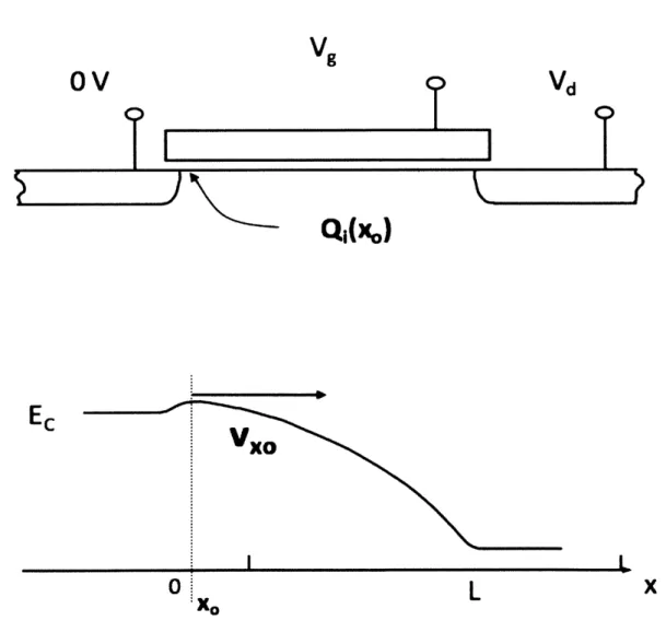
3.1 This figure shows the schematic of an NMOS transistor and the band diagram
corresponding to this transistor. The virtual source, VxO, is at the maximum of the conduction band ... 35
3.2 The beginning of the code for the Verilog-A module of the VS model. Lines
beginning with "parameter" designate model parameters that are modifiable from outside the m odel code... 39 3.3. The equations shown in the text file are most of the equations that govern the static
3.4. This section of the Verilog-A module shows the charge equations and the
differentiation of the intrinsic charges with respect to time... 43
3.5. The circuit diagram shows the entire VS model. The four current sources are equal to the derivatives of the intrinsic terminal charges ... 44
3.6. Ring oscillator schematic using the VS model in Spectre... 45
3.8. Ring oscillator waveform using BSIM in Spectre... 46
List of Tables
Table 2.1 Results of linear circuit simulations...29 Table 2.2 Results of nonlinear circuit simulations... 30
Table 3.1. Comparison between the ring oscillator periods for the VS model using the ballistic (QB) charge model, VS model using velocity saturation charge model, and
Chapter 1
Introduction
Circuit simulation allows circuit designers to successfully validate and optimize their designs. To simulate a circuit, circuit simulators convert the schematic (which can be represented in either graphical or text form) into a system of linear and/or nonlinear differential equations and solve the system. In order to convert a schematic into a system of equations, each component or block in the circuit must be represented by a smaller system of linear and/or nonlinear differential equations. The smaller system for a component or block is known as the compact model for that component or block. In a compact model, the coefficients of the equations are known as the model parameters.
The motivation behind the work presented in this thesis is the importance of compact modeling. As systems become more complex and as devices become smaller, more sophisticated compact models are necessary to describe the behavior of circuits and systems. The contributions presented in this thesis involve the analysis and development of compact models.
The first contribution of this thesis is an analysis of the Verilog-A language as a means of implementing a new class of compact models known as reduced order models.
Reduced order models are a versatile class of mathematical compact models that are relatively accurate and very fast. Verilog-A is language designed for describing compact models, and many commercial simulators support models in Verilog-A. The objective of this work was to determine if Verilog-A is a suitable means of describing reduced order models. The contribution presented in this thesis is an analysis of the feasibility and performance of implementing reduced order models in Verilog-A [1].
The second contribution presented in this thesis is an implementation of a novel
MOSFET model in Verilog-A. As integrated circuits become smaller and more widely
used in different application spaces, fast and accurate compact models for MOSFETs are necessary. Although a number of sophisticated compact models exist, the novel model implemented in this thesis, known as the Virtual Source model, is extremely compact and accurate. Additionally, most of the parameters in the Virtual Source model correspond to physical quantities. The contributions presented in this thesis are the implementation of the model in Verilog-A and examples of circuits simulated using the implementation [2].
Chapter 2
Reduced Order Modeling in
Verilog-A
This chapter presents the background material, methodology, and results for the
contributions related to the performance and feasibility analysis of implementing reduced order models in Verilog-A. Section 2.1 covers the background material on the following topics: circuit simulation, reduced order modeling, the Verilog-A language, and previous work related to compact modeling in Verilog-A. Section 2.2 presents the methodology of the feasibility and performance analysis, and Section 2.3 presents the results of the feasibility and performance analysis.
2.1 Background
This section covers background material and previous work: 2.1.1 covers circuit simulation, 2.1.2 covers reduced order modeling, 2.1.3 covers Verilog-A, and 2.1.4 covers previous work on compact modeling in Verilog-A.
2.1.1 Circuit Simulation
The objective of this sub-section is to present an overview of some topics in circuit simulation. Although this overview is far from exhaustive, it provides the basic description of ideas used later in this chapter.
As stated in Chapter 1, in order to simulate a circuit, a circuit simulator converts a schematic into a system of linear and/or nonlinear ordinary differential equations and
solves the system. The simplest case is when all of the elements have compact models that are linear equations. When a DC simulation is run, the simulator just needs to solve a linear system in order to obtain the node voltages. Figure 2.1 shows an example linear circuit.
In the circuit in Figure 2.1, if all of the nodal equations from Kirchoff's Laws are written, where the variables are the voltages at each node (standard nodal analysis
formulation), then this system of linear equations can be written in the form:
AX
=
1)
(1)
where A is a matrix x is the vector of voltages at each node and b is the right hand side of the system of linear equations. The standard approach to solve the system is to use LU decomposition, where the matrix A is decomposed into upper and lower triangular matrices. Although linear circuits are relatively simple to solve, many circuits contain non-linear elements such as diodes and transistors. Figure 2.2 shows an example of a nonlinear circuit. In this example solving a linear system is insufficient to obtain the nodal voltages.
In order to obtain the nodal voltages in the nonlinear circuit shown in Figure 2.2,
it is necessary to solve a system of nonlinear equations. Although there are a number of methods to solve such a system, the best method is known as Newton's method and is commonly used in circuit simulators.
Newton's method solves a non-linear system by iteratively solving a series of linear systems. The system of equations representing the circuit can be expressed as:
where x is the vector of nodal voltages, F is a nonlinear function of the voltage vectors, and b is the right hand side of the nonlinear system of equations. By solving (2), the nodal voltages, x, can be determined. Newton's method starts with a guess of the
solution, x, and then substitutes the solution into (2). If the solution is acceptable (usually determined by an error tolerance), then the guess is considered sufficient to satisfy the solution. If not, then a new guess is determined through the following equations:
The new guess is then substituted into (2), and the process is repeated, until an acceptable solution is reached. Therefore Newton's method is an iterative process. In (3) and (4), k is the index of the iteration, J(xk)) is the Jacobian of the system, xk is the current guess, x'-') is the guess for the next iteration,f(x(k) is the vector of the function values for the
current guess. The Jacobian of a system is defined as the matrix of derivatives of each function in f with respect to each variable in x. Supposef contains two functions g(x1,x2) and h(xl,x2), then the Jacobian of the system is given by:
____ 011
)rI
)tr21The iterative process described above is repeated until the magnitude of the vector f is small enough. In some instances, the magnitude does not become sufficiently small. These situations are known as non-convergence. Newton's method presented in this section is in its simplest form. A number of modifications exist to improve Newton's method for speed and convergence.
So far, in this sub-section, both examples provided have been for DC analysis, but transient simulations are also very commonly used. If we would like to simulate a circuit using transient analysis, solving systems of linear and non-linear equations is insufficient. It is necessary to solve a system of linear or nonlinear ordinary differential equations. A number of methods exist to solve differential equations, but here we will present the
Backward Euler method as an example.
Suppose we have a differential equation of the form
f
where x is a vector of nodal voltages and f is a nonlinear function of the nodal voltages and time. In order to solve (6), the Backward Euler method approximates the time derivative and rewrites the differential equation as a nonlinear equation
where Xk is the vector of nodal voltages at time k and At is the timestep. In (7), the unknown nodal voltages can be solved for with Newton's Method. In this formulation it
is assumed that the nodal voltages at the previous timestep are known. This is possible because Newton's Method can solve for the initial conditions of the circuit. Once the initial conditions are known, the next time point can be solved for using Backward Euler and Newton's method [3] [4] [5].
2.1.2 Reduced Order Modeling
Compact models for sophisticated devices can become very large (many complicated equations) in order to account for all of the effects the devices. The goal of reduced order modeling is to develop accurate compact models that are significantly simpler than the typical device models. Typical models are often based on the fundamental physics of the devices [6] [7]. Rather than developing models based on the physics of the devices, the reduced order models described in this section are purely mathematical.
The class of reduced order models we present are of the form
d M p(U( M )x (W)
-x ( }M U M
di
q(u(fe).x( t))
for continuous time systems, and
p(U ].u tI- 1...u I-n.xu [ t .x -1....xf:-nu )
x[t+1|-~
j.jl.
t-I~[1xzl~
ln
g(ul I].UlIt -I ]....,u[ I -nI, x it I. itI- I,...,'X I[ -n]l)
for discrete time systems. In both types of the reduced order models, po and qO are polynomial functions of x(t) and u(t), which are the state and input of the system.
Currently methods of determining reduced ordered models are determined through system identification and have been shown to accurately describe the behavior of power amplifiers and MEMS devices [8].
2.1.3 The Verilog-A Language
Verilog-A is a language for describing analog hardware. The language allows circuit designers to create modules (behavioral blocks in a circuit) and define the behavior of the modules through specifying the mathematical relationships between the currents and voltages terminals of the modules. Although the language is capable of describing thermal and fluidic systems, the information presented in this section will only describe the use of Verilog-A for electrical systems; in particular how Verilog-A is used to create
modules in circuit simulators. In order to illustrate how Verilog-A is used in circuit simulators an example is shown in Figures 2.3 and 2.4. Figure 2.3 shows the circuit schematic of a Verilog-A module, and Figure 2.4 shows the Verilog-A code for the module [1].
Figure 2.3 This circuit schematic, which is drawn in Spectre, shows a Verilog-A block called vaexample.
include "constants.vams" include "disciplines .vams~
module vaexample(a,b); electrical a,b; analog begin I(a,b)C+V(a,b)*(1/10); end endmodule
Figure 2.4 contains all of the code that describes the Verilog-A module in the circuit schematic in Figure 2.3. Although this module is very simple, it shows the fundamental structure of how Verilog-A modules are written. The two lines that begin with " 'include " specify the Verilog-A libraries that are used in the remainder of the code. The lines beginning with "module" and "endmodule" specify the beginning and end of the module. All of the code describing the behavior is between these two lines. The lines beginning with "analog begin" and "end" specify the analog behavioral section.
All of the equations governing the behavior of the block are specified inside the analog
behavioral section. Usually, the only items specified outside of the analog block, but within the module are terminals, variables, or parameters. In the line
"I(a,b)<+V(a,b)*(l/l0);", the symbol "<+" means that the two values are fixed to one another. Verilog-A requires that this symbol is used when setting the value of a current or a voltage of an electrical terminal or node. For other variables the standard "=" is used. Most standard mathematical functions such as exponentials, logarithms, and polynomials are supported by Verilog-A and can be used in the analog behavioral section
2.1.4 Previous Work on Compact Modeling in
Verilog-A
In order to understand how Venilog-A has been previously used in compact modeling a search of previous compact models developed in Verilog-A was conducted. A major source of Verilog-A models is The Designers Guide Community. This website contains a number of Verilog-A models available for download in addition to a forum, which is moderated by Verilog-A experts.
After examining the models available for download, we found that all of these models were models based directly on the physics of the device. Currently no purely mathematical reduced order models were found [10].
2.2
Methodology
This section covers the methodology of determining whether Verilog-A is a suitable language for implementing reduced order models. In order for Verilog-A to be a suitable language for implementing the reduced order models, two requirements must be satisfied. First, the features of the Verilog-A language must be capable of handing the reduced order models. Second, if Verilog-A modules of the reduced order models are
implemented in Spectre [9], it is necessary that the simulation speed of these modules is sufficiently fast. More specifically, if a circuit is simulated in Spectre and the reduced
order model for this circuit, which is implemented in Verilog-A, is also simulated in Spectre, the reduced order model should be substantially faster.
Determining if the features of the language are capable of handing reduced order models involved examining the documented features of the language and determining the appropriate functions to describe the reduced order models.
Determining if the Verilog-A modules are sufficiently fast involved comparing the speed of circuits simulated directly in Spectre compared to the speed of a Verilog-A module of the same circuit. The main objective was to determine if using Verilog-A
resulted in a slower simulation due to the Verilog-A language.
2.3 Results
Section 2.3.1 covers the results related to the feasibility analysis of using Verilog-A to implement reduced order models. Section 2.3.2 covers the results related to the speed tests in Verilog-A.
2.3.1 Verilog-A Feasibility Analysis
As previously stated the reduced order models are of the form,
d
X ()=
p(U ( X M)di q( ).X )
q ,Utt.ui-
I
fXIt tn.'1,xtt-I lfor the discrete case. In order to effectively implement reduced order models in Verilog-A, it is necessary to ensure that Verilog-A contains the appropriate features in order to do so. The key features necessary in the language are the ability to implement derivatives and time delays. As previously discussed, polynomials and other mathematical functions are available in Verilog-A.
It was found that a time delay is possible in Verilog-A using the transitiono function. An example of the transition() function is shown in Figure 2.5. It also was found that expressing derivatives is possible thought the ddt() and into functions. An example is shown in Figure 2.6. Using the functions transisiono, idtO, and ddt(), in addition to polynomial functions, it is possible to express reduced order models in Verilog-A [1]. include "constants.vams" include "disciplines.vams" module nonlinearveril3(inp,inn,outp,outn); electrical inp,inn,outp,outn; analog begin @(initial step)begin V(outp,outn)<+1; end V(outp,outn)<+ transition(V(outp,outn),[0.000001])+5+V(inpinn); end endmodule
Figure 2.5. Example of the transitiono function. In this example, V(outp,outn) is delayed by 0.000001 s.
include "constants.vams" include "disciplines.vams~ module nonlinearveril6(inp,inn,outp,outn); electrical inp,inn,outp,outn; analog begin @(initial step)begin V(outn,outp)<+ 0; end
V(outn,outp),+ IdtlV(inn,Inp) - (v(outn,outp)/(0.0000000001+v(outn,outp)*V(outnoutp)))); end
endmodule
Figure 2.6. An example of the idto function used to integrate a function of the voltages across the terminals in the module.
2.3.2 Verilog-A Speed Analysis
The speed analysis of Verilog-A was conducted to determine if the Verilog-A language substantially slows down transient simulations. From observing simulations in Spectre, we believe that Verilog-A in Spectre is compiled. This means that before a transient analysis begins, the symbolic derivatives (for the Jacobian) for each function in the Verilog-A module are calculated. Consequently, if Verilog-A runs more slowly it is not a result of being an interpreted language. In order to determine if Verilog-A does slow
down simulations, linear and nonlinear circuits were both simulated in Spectre. For both the linear and non-linear circuit, the same circuit was simulated using Spectre
components and also as a Verilog-A module.
For the linear circuit, transient analyses were run in Spectre with a 1 GHz input voltage of 2 V, and transient times of 100 us, 250 us, and 500 us. For both the Verilog-A version and the version directly implemented in Spectre, the number of timesteps in the transient simulation were almost identical (within 1% of each other), so any overall difference in simulation time is not due to more timesteps. Table 2.1 shows the results of the linear circuit.
Transient Analysis Spectre Circuit Verilog-A Circuit
Time(us) Simulation Time (s) Simulation Time (s)
100 67.35 83.07
250 168.03 200.29
500 336.36 398.63
Table 2.1 Results of linear circuit simulations.
For the nonlinear circuit, transient analyses were also run in Spectre with a 1 GHz input voltage of 2 V, and transient times of 100 us, 250 us, and 500 us. For both the Verilog-A version and the version directly implemented in Spectre, the number of timesteps in the transient simulation were almost identical (within 1% of each other), so
any overall difference in simulation time is not due to more timesteps. Table 2.2 shows the results of the nonlinear circuit.
Transient Analysis Time Spectre Circuit Verilog-A Circuit
(us) Simulation Time (s) Simulation Time (s)
100 59.70 67.61
250 149.60 170.25
500 299.20 399.91
Table 2.2 Results of nonlinear circuit simulations.
Based on the results of the simulations, the Verilog-A implementation in Spectre runs approximately 1.2x slower in the linear case and 1.3x slower in the non-linear case. For the linear and nonlinear circuit, the number of timesteps is almost identical for the Verilog-A implementation and the implementation using Spectre elements. Because of this, we conclude that the time difference is not due to more timesteps, but the Verilog-A simulation taking more time at each timestep. Three reasons can cause this difference: more time spent calculating the Jacobian, more time evaluating the function in Newton's method, or taking more Newton iterations. While it is possible that more Newton iterations has an effect, since the nonlinear Verilog-A implementation is slightly slower than the linear Verilog-A implementation, it is unlikely that the number of iterations is the primary differentiating factor. Therefore, based on these tests we conclude that the
primary reason that Verilog-A is slower in Spectre is because the evaluation of the Jacobian and the functions take longer.
Chapter 3
Implementation of a Novel
MOSFET Model in Verilog-A
This chapter presents the background material, methodology, and results for the contributions related to the implementation of a novel MOSFET model in Verilog-A. Section 3.1 covers the background material on the novel MOSFET model, which is known as the Virtual Source model. Additionally, Section 3.1 covers appropriate background material on charge partitioning models in transistor devices and some background work on other Verilog-A MOSFET models. Section 3.2 presents the methodology of the implementation of the model, and Section 3.3 presents the results of circuit simulations using the Verilog-A implementation of the Virtual Source model.
3.1 Background
This section covers background material and previous work: 3.1.1 covers background material on the Virtual Source model, 3.1.2 covers background material on charge
distribution models, and 3.1.3 covers previous work on MOSFET models and the implementation of MOSFET models in Verilog-A.
3.1.1 The Virtual Source Model
The Virtual Source model (VS model) is a MOSFET model that was first published in
2009. In the first publication of the model, the model only contained static behavior.
This sub-section will present an overview of the static VS model [2].
The equations that govern the static behavior of the VS model calculate the drain to source current of the MOSFET for a specific set of terminal voltages and model parameters. The core idea behind the VS model is to determine the drain to source current by calculating the charge density and electron velocity at the virtual source of the device. As shown in Figure 3.1, the virtual source of the device is the maximum value of the conduction band in the device.
In order to determine normalized drain to source current of the transistor, the model calculates the product of three terms: the charge density at the virtual source, the
charge velocity of the virtual source, and a non-saturation factor:
In the above equation W is the width of the device and a parameter of the model;
v
is the virtual source velocity, which is also a device parameter. The expression Qr, is thecharge density at the virtual source, and F, is a factor that accounts for non-saturation behavior. These two expressions are given by the following equations:
- 1~j>. - (1 *,. - (~(~DIj
1K. - '
(10)
In the above expressions, Cg, n,
#,,
are model parameters corresponding to the gate capacitance, the subthreshold swing, and thermal voltage. The parameters c andp
are fitting parameters. The additional terms in (9) and (10) are given by:F - I
(11)
VD S . I - - F ) +1,2
13
/I(1 4
I *1 hi - 1141(15)
(16)
(9)
{
(
))
I 'G IPS UsThe terms L, and t are model parameters corresponding to the effective length and the mobility of the transistor, respectively. The terms Rs and Rd are the drain and source resistances of the device. The term 8 is a model parameter that accounts for the drain induced barrier lowering, and VTO [2].
Vg
oV
Vd
Q
1
(X
0
)
Vxo
L
X0X
Figure 3.1 This figure shows the schematic of an NMOS transistor and the band diagram corresponding to this transistor. The virtual source, Vx., is at the maximum of the
conduction band.
3.1.2 Charge Partition Models for Transistors
One contribution presented later in this chapter is the addition of dynamic behavior to the Verilog-A implementation of the VS model. This sub-section provides the necessary background material to understand this contribution.
As described in 3.1.1, the VS model in its original form only contained equations to describe the static behavior of the model. In order to account for the dynamic behavior
it is necessary to account for the intrinsic charges associated with the drain, gate, source, and body of the transistor. The basic charge model used to implement dynamic behavior in the VS model is based on the charge description in [12]. The following equations show the charges associated with each terminal:
6 + 12V + 8q2 + 4q3 Qs i 15(1 + 1)2 4 + 8q + 121,2 + 6r3 QD -inv- 15(1 +1)2
QG
= -(QB +QD
+QS)
Vos V1 = Vos_ VI 0, Vos > VD'sa1+
Y V GS-VT2
,= 1 a -V1 2 + + q2 QH -W LCoxyv "0 + VsH - Qinv - 3 1These equations are the basis for the classical intrinsic charge models. QD, QS, QG, and
QB correspond to the intrinsic charge associated with the drain, source, gate and body of
the transistor. The term y is the body factor, which is a model parameter. W, L and Cox are also model parameters corresponding to the width, length, and gate capacitance of the device. The quantity Qinv is the same as Qref in subsection 3.1.1 [11].
3.1.3 Previous Work on MOSFET Compact
Modeling in Verilog-A
This sub-section briefly reviews previous work conducted on MOSFET compact modeling in Verilog-A. A major resource for Verilog-A developers is The Designer's
Guide Community. A number of previously developed Verilog-A models are available for download, and a forum exists where a number of experts in Verilog-A answer questions. In order to review previous work on MOSFET modeling in Verilog-A, the models available for download were examined. Additionally standard industrial models
such as BSIM and PSP were examined [6] [7] [10].
The main transistor model found on The Designer's Guide Community Website was the MOS 11 [10]. This model contains more than double the number of parameters in the VS model. BSIM and PSP, which are currently industrial standards, contain over
only contains around 20 parameters, and almost all of them are physical, the Verilog-A implementation of the VS model can be an asset to circuit and device designers.
3.2 Methodology
This section covers the methodology of the Verilog-A implementation of the VS model:
3.2.1 covers the implementation of the static behavior and 3.2.2 covers the
implementation of the dynamic behavior. The full Verilog-A code for the VS model can be found in Appendix A.
3.2.1 Static Behavior Implementation
In this section the static model implementation in Verilog-A is described. For a background on the Verilog-A language please see section 2.1.
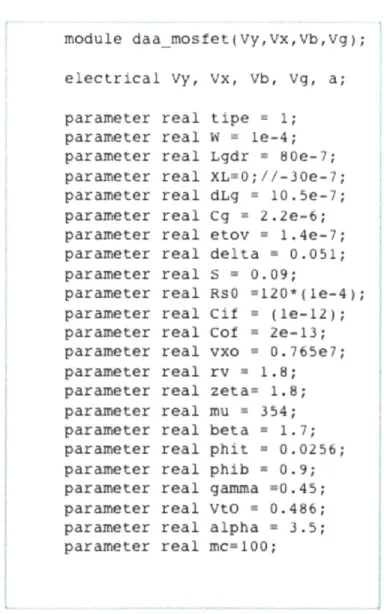
In order to implement the DC behavior of the model, a Verilog-A module was created with the terminals corresponding to the drain, gate, source, and body of the transistor. Figure 3.2 shows the beginning of the Verilog-A module, which is named daamosfet. The terminals are named Vy, Vx, Vb, and Vg, which correspond to the
source, drain, body, and gate of the transistor. All of the lines that begin with "parameter real" specify the parameters of the model such as transistor length and width. These parameters are accessible from outside the code, so the values can be modified directly
from the circuit schematic. The four final lines in the text file are the list of all of the internal variables used in the model; none of these variables are externally modifiable.
module daamostet(Vy,Vx,Vb,Vg);
electrical Vy, Vx, Vb, Vg, a;
parameter real tipe = 1;
parameter real W = le-4;
parameter real Lgdr m 80e-7; parameter real XL-0;//-30e-7;
parameter real dLg 10.5e-7;
parameter real cg 2.2e-6;
parameter real etov 1.4e-7;
parameter real delta 0.051;
parameter real S = 0.09;
parameter real RsO ul20*(Ie-4); parameter real Cif a (1e-12);
parameter real Cof = 2e-13;
parameter real vxo = 0.765e7;
parameter real rv = 1.8;
parameter real zeta= 1.8;
parameter real mu = 354;
parameter real beta = 1.7;
parameter real phit w 0.0256;
parameter real phib = 0.9;
parameter real gamma =0.45; parameter real Vto a 0.486;
parameter real alpha = 3.5;
parameter real mc-100;
Figure 3.2 The beginning of the code for the Verilog-A module of the VS model. Lines beginning with "parameter" designate model parameters that are modifiable from outside the model code.
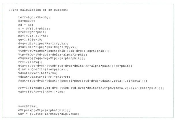
In addition to specifying the terminals, model parameters and internal variables, it is necessary to specify all of the equations that govern the model. All of equations are in the analog behavior section of the Verilog-A module. Figure 3.3 shows a section of the analog behavior [1].
//The calculation of dc current:
Let f =Lgdr+XL-dLg; Rs=RSO/W; Rd Rs; n =S/(2.3*phit); Qref=Cg*n*phit; me-(9.le-31)'mc; ge=1.602e-19; dvg(dir*tipe)*Rs*I(vy,Vx); dvd-(dir*tipe)*(Rs+Rd)*I(vy,vx); vtobuVto+gamma*(sqrt(phib-(vbb-dvg) )-sqrt(phib)); vtp-vtob-(Vd-dvd)*delta-alpha/2*phit; evg-exp((Vqg-dvg-vtp)/(alpha*phit)); rFF1/(1+evg);
eta=( (Vgg-dvg)-(vtob-(vd-dvd)*delta-FF*alpha*phit ))/(n*phit); Qinv = Qref*ln(1+exp(eta));
Vdsatsavxo*(Leff )/mu; VdsatVdsats*(1-FF)+phit*FF;
Fsat=((Vd-dvd)/Vdsat)/(pow((1+pow(((Vd-dvd)/Vdsat),beta)),(1/beta)));
FFv- I/(1+ exp( (vgg-dvg-(vtob-(vd-dvd)*delta+phit-poyw(zeta,2)/2) )/(zeta*ph it)));
VxO(FFV/rv+( 1-FFv) )*Vxo;
vuvxO*Fsat;
eVtpmexp(-Vtp/(alpha*phit)); Cov a (0.345e-12/etov)*dLg/2+Cof;
Figure 3.3. The equations shown in the text file are most of the equations that govern the static behavior of the VS model.
3.2.2 Dynamic Behavior Implementation
Unlike the implementation of the static behavior, the implementation of the dynamic behavior of the VS model was less straightforward because there are multiple possible methods of implementation.
The reason there are multiple methods to implement the dynamic behavior is that it is possible to use either the capacitances or charges. If capacitances are used, the voltage dependent capacitances will need to be calculated for each pair of terminals, so the entire capacitive matrix will need to be calculated. By using the capacitances, the
dynamic behavior is effectively modeled by voltage dependent capacitors connected between each terminal. If charges are used, the rate of change of these charges with respect to time will result in intrinsic currents going into each terminal, so in order to
calculate these currents it is necessary to differentiate the intrinsic charges with respect to time. Using either capacitances or charges results in the same overall effect; just the method of modeling will be different. It was chosen to use charges, because of the
simplicity of implementation and the ability to easily change charge models.
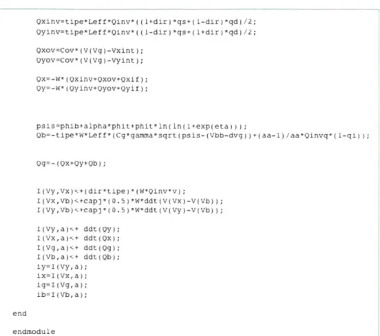
Rather than calculating the full capacitive matrix of all the capacitances between each terminal in the transistor, charges were used to implement the dynamic behavior. In order to use charges to model the dynamic behavior, first the charge equations were integrated into the Verilog-A module. Figure 3.4 shows an image of the charge equations in the Verilog-A code. In addition to integrating the charge models, it is also necessary to differentiate the charges in order to determine the intrinsic currents. The Verilog-A time
and the current between each terminal and the internal node is set equal to the derivative of the intrinsic charge corresponding to that terminal. Since all of the charges add to zero, conservation of charge is not violated. A circuit representation of how to charges were integrated is shown in Figure 3.11. The current resulting from the time derivative of each intrinsic charge is represented by a current source.
The reason the ddt() function was used instead of differentiating the analytical charge equations is that the implementation is simpler and allows for more flexibility in the charge models. If analytical differentiation is used, and we would like to modify the charge models, then it will be necessary to determine all of the derivatives again. Using the ddto function, the charge equations can be easily modified. Because some of the expressions in the charge equations contain discontinuities, safe functions were used to make certain functions smoother [13].
In addition to using the classical charge models for the intrinsic charges, which were described in Section 3.1.2, charge models which represent ballistic and velocity saturation were also included in the model [12].
Qxinv-tipe*Left*Qinv*((1+dir)*qs+(1-dir)*qd)/2; Oyinvetipe*Leff*Qinv*((1-dir)*qs+(1+dir)*qd)/2; Qxov=Cov*(V(Vg)-Vxint); QyOv-Cov*(V(Vg)-Vyint); Qx=-W*(Qxinv+Qxov+Qxit); Qy=-W*(Qyinv+Qyov*Qyit); psis-phib+alpha*phit+phit*1n(In(1+exp(eta)) ); Ob--tipe*W*Leff*(Cg*gamma*sgrt(psis-(Vbb-dvg))+(aa-1)/aa*Qinvg*(1-qi)); Qg-(QXO+y+Qb); I(Vy,Vx)z+dir*tipe)*(W*Qinv*v); I(Vx,Vb)+capj*(0.5)*W*ddt(V(Vx)-V(Vb)); I(Vy,Vb).+capj*)0.5)*W-ddt(V(Vy)-V(vb)); I(Vy,a)C+ ddt(Oy); i(Vx,a)C+ ddt(ox); I(Vg,a),,+ ddt(og); I(Vb,a)C+ ddt(Qb); iy=1(Vy, a); ixm1(Vx,a); ig=1(vg, a); ib-1(Vb, a); end endmodule
Figure 3.4. This section of the Verilog-A module shows the charge equations and the differentiation of the intrinsic charges with respect to time.
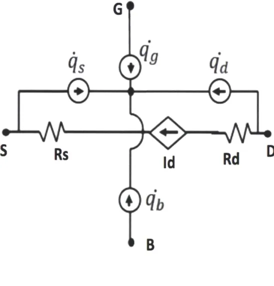
G
09
S
Rs
qd
Id
Rd
D
'b
B
Figure 3.5. The circuit diagram shows the entire VS model. The four current sources are equal to the derivatives of the intrinsic terminal charges.
3.3 Results
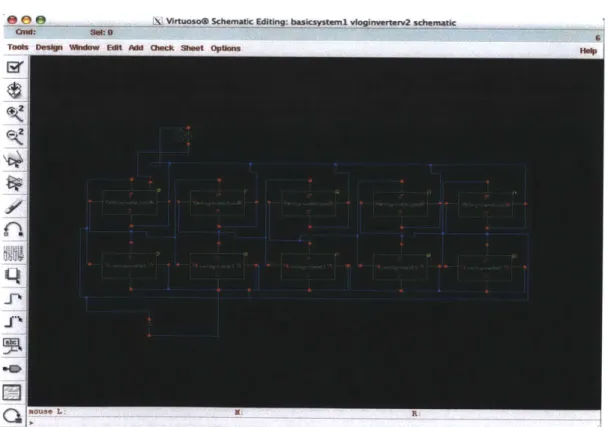
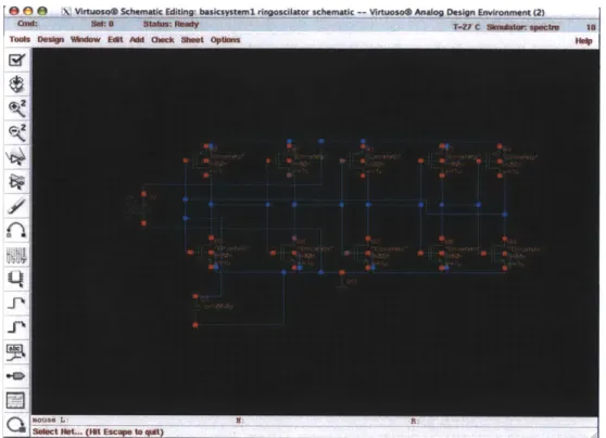
In order to test and validate the model, ring oscillators were designed with the Verilog-A implementation of the VS model. Our collaborators fit the VS model to match a model file of BSIM [6]. Currently our collaborators use a method that combines mathematical optimization and observation in order to fit the VS model to experimental data or data from another MOSFET compact model. Once the appropriate parameters for the VS model were obtained in order to match BSIM, ring oscillators were designed with the VS model and the BSIM model. Figures 3.6 and 3.7 show the schematics of the ring
oscillators in Spectre. Figures 3.8 and 3.9 show the waveforms of the two ring oscillators.
e e X WtosoO Schematic Editisgas tamivl ognvefer2 schematic
Tools Desi R ulw Edi lA Or chuat Optinsi
* a a Virtuoso Schenatic Editing: bascsysteml rnosciator schematic -- Virtuoso Analog Design Environment (2)
One : a ad, 3 -- "Redy T-27 C anddwar spectre i0
Tos On Vndow Et Add Check 9h sot Options Hp
LM
-4
nous L.
Select Wt..t( Escape to *A)
Figure 3.7. Ring oscillator schematic using BSIM in Spectre.
196ps1 1.3017V
>
> Selection accumulate mode on.
Figure 3.9. Ring oscillator waveform using BSIM in Spectre.
Although the objective of simulating ring oscillators with BSIM and the VS model was to test and validate the VS model, this approach has limitations. BSIM contains a number of parameters that describe the capacitances in the device, and these capacitance parameters in BSIM do not directly correspond to the parameters that govern the capacitances in the VS model. For this reason, in order for the periods of the
oscillations to in the BSIM and VS ring oscillators to come very close to one another, it was necessary to tweak the capacitances in the VS model. The capacitances that were tweaked were the inner and outer fringing capacitances. Given this limitation, visual
analysis of Figures 3.7 and 3.8 show a good match between the models. In order to further test the VS model, it was fitted to experimental data.
The VS model was fitted to experimental data by our collaborators, and using the fitted parameters ring oscillators of different fan-out values were designed and simulated in Spectre. Because the VS model contains different charge models for the intrinsic charges depending on whether classical, ballistic, or velocity saturation is assumed, the ring oscillators have different periods depending on which charge model is used. Table
3.1 shows a comparison between the experimental data. Overall, this data shows a
reasonably good match between the VS model and experimental data. In this case, again, the capacitances needed to be tweaked in order to obtain a reasonably good match [12]. Further work is required to fully automate the fitting of the capacitance in the VS model
FO
Measured
QB
Vsat
1
4.90
4.79
4.93
3
9.99
9.98
10.26
5
15.38
15.32
15.63
7
20.78
20.87
21.2
Table 3.1. Comparison between the ring oscillator periods for the VS model using the ballistic (QB) charge model, VS model using velocity saturation charge model, and measured data.
Chapter 4
Conclusion
This thesis presents two contributions related to compact modeling in Verilog-A. First, feasibility and performance analyses were conducted to determine if Verilog-A is a suitable language for implementing reduced order models. Second, a novel MOSFET model was implemented in Verilog-A.
It was found that Verilog-A is a suitable language for implementing reduced order models in the Spectre simulator. Not only is the Verilog-A language capable of handing the models, but also the Verilog-A simulation speed in Spectre is sufficiently fast.
The Virtual Source model was implemented in Verilog-A and tested in Spectre. Ring oscillators were simulated and good fitting was found between the VS model and experimental data.
Appendix A
The Verilog-A Implementation of
the Virtual Source Model
// VerilogA for daamosfet, daamosfet, veriloga
'include "constants.vams" 'include "disciplines.vams" module daa-mosfet(Vy,Vx,Vb,Vg); electrical Vy, Vx, Vb, Vg, a; parameter parameter parameter parameter parameter parameter parameter parameter parameter parameter parameter parameter parameter parameter parameter parameter parameter parameter parameter parameter parameter parameter parameter real real real real real real real real real real real real real real real real real real real real real real real tipe = 1; W = le-4; Lgdr = 80e-7; XL=O;//-30e-7; dLg = 10.5e-7; Cg = 2.2e-6; etov = 1.4e-7; delta = 0.051; S = 0.09; Rs0 =120*(le-4); Cif = (le-12); Cof = 2e-13; vxo = 0.765e7; rv = 1.8; zeta= 1.8; mu = 354; beta = 1.7; phit = 0.0256; phib = 0.9; gamma =0.45; VtO = 0.486; alpha = 3.5; mc=100;
real Rd, Vgg, Vbb, Vd, VtOb, n, Qref, vv, FF, Qinv, Vdsats, Vdsat, Fsat, dvg, dvd, Vtp,eVg,eta,v,eVtp,xden,qsqdQxinv,Qyinv,dir,FFint,Qxif,Qyif,Qxov,Qyo v,Cov,psis,FFv,vxO,sign,Rs,Leff,Qg, Qx, Qy, Qb,VtOx,VtOy,FFx,FFy,Vgt,aa,Vdsatq,Fsatq,qi,Qinvq,Vxint,Vyint,meqeqs, qdc,kq,qsb,qdb,kFsatq,etai,qdtemp,QinvidQinv,igib,ix,iy,capj,Ec,vdssm oothcapA,capB,Ap,Bp,qsvO,qdvO,qsv,qdv,kvsatq;
analog function real smoothabs; input x, smoothing; real x,smoothing; begin smoothabs=sqrt(x*x+smoothing); end endfunction
analog function real smoothmax; input c,b,smoothing; real cb,smoothing; begin smoothmax=0.5*(c+b+smoothabs(c-b,smoothing)); end endfunction
analog function real smoothsign; input x, smoothing; real xsmoothing; begin smoothsign=x/sqrt(x*x+smoothing); end endfunction
analog function real safesqrt; input x, smoothing; real x,smoothing; begin safesqrt=sqrt(O.5*(smoothabs(x,smoothing)+x)+1e-16); end endfunction
analog function real safeexp; input x, maxslope; real xmaxslopebreakpoint; begin breakpoint=ln(maxslope); if(x<=breakpoint) safeexp=exp(x);
else safeexp = maxslope+maxslope*(x-breakpoint);
end endfunction
analog function real safeln; input x,smoothing; real x,smoothing; begin end endfunction safeln=ln(O.5*(smoothabs(x,smoothing)+x)+1e-16); analog begin if (tipe*(V(Vg)-V(Vx))>tipe*(V(Vg)-V(Vy))) begin Vd=abs(V(Vy)-V(Vx)); end else Vd=abs(V(Vx)-V(Vy)); if (tipe*(V(Vg)-V(Vx))>tipe*(V(Vg)-V(Vy))) begin Vgg=tipe*(V(Vg)-V(Vx)); end else Vgg=tipe*(V(Vg)-V(Vy)); if (tipe*(V(Vg)-V(Vx))>tipe* dir=1; end else dir=-1; (V(Vg)-V(Vy))) begin if (tipe*(V(Vb)-V(Vx))>tipe*(V(Vb)-V(Vy))) begin Vbb=tipe*(V(Vb)-V(Vx)); end else Vbb=tipe*(V(Vb)-V(Vy)); if (tipe==1) begin capj=0.158*(le-ll); end else capj=0.1*(le-ll);
//The calculation of dc current: Leff=Lgdr+XL-dLg; Rs=RsO/W; Rd = Rs; n = S/(2.3*phit); Qref=Cg*n*phit; me=(9.le-31)*mc; qe=1.602e-19; dvg=(dir*tipe)*Rs*I(Vy,Vx); dvd=(dir*tipe)*(Rs+Rd)*I(Vy,Vx); VtOb=VtO+gamma*(sqrt(phib-(Vbb-dvg))-sqrt(phib)); Vtp=VtOb-(Vd-dvd)*delta-alpha/2*phit; eVg=exp((Vgg-dvg-Vtp)/(alpha*phit)); FF=1/(1+eVg); eta=((Vgg-dvg)-(Vtob-(Vd-dvd)*delta-FF*alpha*phit))/(n*phit); Qinv = Qref*ln(1+exp(eta)); Vdsats=vxo*(Leff)/mu; Vdsat=Vdsats*(1-FF)+phit*FF; Fsat=((Vd-dvd)/Vdsat)/(pow((1+pow(((Vd-dvd)/Vdsat),beta)),(1/beta))); FFv=l/(1+exp((Vgg-dvg-(VtOb-(Vd-dvd)*delta+phit*pow(zeta,2)/2))/(zeta*phit))); vxO=(FFv/rv+(1-FFv))*vxo; v=vxO*Fsat; eVtp=exp(-Vtp/(alpha*phit)); Cov = (0.345e-12/etov)*dLg/2+Cof;
//The calculation of charges:
aa=l+gamma/(2*sqrt(phib-Vbb+dvg)); qi=(2/3)*(1+x+pow(x,2))/(1+x); Qinvq=Qinv*qi; Vxint=V(Vx)+(tipe*dir)*dvg; Vyint=V(Vy)-(tipe*dir)*dvg; Vdsatq=sqrt(pow(3*phit,2)+pow((Vgt/aa),2)); Fsatq=((Vd-dvd)/Vdsatq)/pow((1+pow(((Vd-dvd)/Vdsatq),beta)),(1/beta)); VtOx=VtO+gamma*(sqrt(phib-(tipe*(V(Vb)-Vxint)))-sqrt(phib)); VtOy=VtO+gamma*(sqrt(phib-(tipe*(V(Vb)-Vyint)))-sqrt(phib)); FFx=1/(l+exp((tipe*(V(Vg)-Vxint)-(VtOx-(Vd-dvd)*delta-alpha/2*phit))/(alpha*phit))); FFy=l/(1+exp((tipe*(V(Vg)-Vyint)-(VtOy-(Vd-dvd)*delta-alpha/2*phit))/(alpha*phit))); Qxif=Cif*FFx*(V(Vg)-Vxint); Qyif=Cif*FFy*(V(Vg)-Vyint);
x=(1-Fsatq);
den=15*pow((1+x),2);
qsc=(6+12*x+8*pow(x,2)+4*pow(x,3))/den; qdc=(4+8*x+12*pow(x,2)+6*pow(x,3))/den;
//advanced charge models start here //ballistic transport kq=sqrt(2*(qe/me)*(Vd-dvd))/vxo*le2; qsb=((1/kq+1/kq/kq)*ln(1+kq)-1/kq); qdb=(1/kq/kq*(kq-ln(1+kq))); if (mc>99) begin kFsatq=O; end else kFsatq=1; if (kFsatq==1) begin kvsatq=O; end else kvsatq=1; Vgt=Qinv/Cg; //velcocity saturation Ec=l*vxo/mu; vdssmooth=Vgt/aa*2/(1+safesqrt(smoothmax(1,1+2*Vgt/aa/Ec/Leff,smo othing),smoothing))*Fsatq; capA=pow(aa,2)*pow(vdssmooth,2)/(12*Vgt-6*aa*vdssmooth); capB=(5*Vgt-2*aa*vdssmooth)/(10*Vgt-5*aa*vdssmooth); Ap=capA*(1+vdssmooth/(Leff)/Ec); Bp=capB*((pow(vdssmooth,2)*aa)/(2*Ec*Leff*(5*Vgt-2*vdssmooth*aa))+1); qsvO=Vgt/2-vdssmooth/6+Ap*(1-Bp); qdvO=Vgt/2-vdssmooth/3+Ap*Bp; qsv=qsvO/Vgt; qdv=qdvO/Vgt;
//kFsatq=O for classical D/D and =1 for ballistic
qs=((1-kvsatq)*qsc+kvsatq*qsv)*(1-kFsatq*Fsatq)+qsb*kFsatq*Fsatq;
qdtemp=((1-kvsatq)*qdc+kvsatq*qdv)*(1-kFsatq*Fsatq)+qdb*kFsatq*Fsatq;
I/ DIBL effect on drain charge calculation
etai=((Vgg-dvg)-(VtOb-(Vd-dvd)*0-FF*alpha*phit))/(n*phit); Qinvi=Qref*ln(1+exp(etai));
qd=(qdtemp-(l-FF)*qi*dQinv/Qinv); Qxinv=tipe*Leff*Qinv*((I+dir)*qs+(l-dir)*qd)/2; Qyinv=tipe*Leff*Qinv*((l-dir)*qs+(l+dir)*qd)/2; Qxov=Cov*(V(Vg)-Vxint); Qyov=Cov*(V(Vg)-Vyint); Qx=-W*(Qxinv+Qxov+Qxif); Qy=-W*(Qyinv+Qyov+Qyif); psis=phib+alpha*phit+phit*ln(ln(l+exp(eta))); Qb=-tipe*W*Leff*(Cg*gamma*sqrt(psis-(Vbb-dvg))+(aa-1)/aa*Qinvq*(l-qi)); Qg=-(Qx+Qy+Qb); I(VyVx)<+(dir*tipe)*(W*Qinv*v); I(VxVb)<+capj*(0.5)*W*ddt(V(Vx)-V(Vb)); I(VyVb)<+capj*(0.5)*W*ddt(V(Vy)-V(Vb)); I(Vya)<+ ddt(Qy); I(Vxa)<+ ddt(Qx); I(Vga)<+ ddt(Qg); I(Vba)<+ ddt(Qb); iy=I(Vya); ix=I(Vxa); ig=I(Vga); ib=I(Vba); end endmodule
Bibliography
[1] Verilog-A Language Reference Manual. Version 1.0. Open Verilog International, 1996.
[2] A. Khakifirooz, O.M. Nayfeh, and D. Antoniadis. A Simple Semiempirical Short-Channel MOSFET Current-Voltage Model Continuous Across All Regions of Operation and Employing Only Physical Parameters. Electron Devices, IEEE Transactions on Electron Devices, Volume 56, Issue 8, Aug. 2009 Page(s):1674 - 1680.
[3] G. Recktenwald. Numerical Methods with Matlab. Prentice Hall, 2000.
[4] K.G. Nichols et al. Overview of SPICE-like circuit simulation algorithms. IEE Proc.-Circuits Devices Syst. Vol. 141, No. 4. August 1994. Page(s): 242-250.
[5] A. Sangiovanni-Vincentelli, P. C. McGeer, A. Saldanha, "Verification of Electronic
Systems", 33rd Design Automation Conference, 1996.
[6] BSIM. http://www-device.eecs.berkeley.edu/bsim/?page=BSIMCMG .
[7] PSP. http://pspmodel.asu.edu/introduction.htm.
[8] B. N. Bond, Z. Mahmood, R. Sredojevic, Y. Li, A. Megretski, V. Stojanovic, Y.
Avniel, and L. Daniel, "Compact Modeling of Nonlinear Analog Circuits using System Identification via Semi-Definite Programming and Robustness Certification," submitted to IEEE Transaction on Computer Aided Design of Integrated Circuits and Systems in June 2009.
[10] Designer's Guide Community. http://www.designers-guide.org/.
[11] Y. Tsividis. Operation and Modeling of the MOS Transistor. Boston :WCB
McGraw-Hill, 1999.
[12] L. Wei, 0. Mysore, and D. Antoniadis. Virtual-Source-Based Self-Consistent Current and Charge FET Models: From Ballistic to Drift-Diffusion Velocity-Saturation Operation. IEEE Transactions on Electron Devices, Vol. 59. No. 5. May 2012.
[13] The safe functions used are based on discussions with Professor Jaijeet
![Figure 2.1. An example of a linear circuit from Spectre [9].](https://thumb-eu.123doks.com/thumbv2/123doknet/14398960.509652/17.918.258.589.649.932/figure-example-linear-circuit-spectre.webp)