HAL Id: cea-01056964
https://hal-cea.archives-ouvertes.fr/cea-01056964
Submitted on 21 Aug 2014HAL is a multi-disciplinary open access
archive for the deposit and dissemination of sci-entific research documents, whether they are pub-lished or not. The documents may come from teaching and research institutions in France or abroad, or from public or private research centers.
L’archive ouverte pluridisciplinaire HAL, est destinée au dépôt et à la diffusion de documents scientifiques de niveau recherche, publiés ou non, émanant des établissements d’enseignement et de recherche français ou étrangers, des laboratoires publics ou privés.
Investigation of nanoelectrodes by Transmission
Electron Microscopy
M.S. Kabir, S.H.M. Persson, Yimin Yao, Jean-Philippe Bourgoin, Serge
Palacin
To cite this version:
M.S. Kabir, S.H.M. Persson, Yimin Yao, Jean-Philippe Bourgoin, Serge Palacin. Investigation of nanoelectrodes by Transmission Electron Microscopy. MRS Proceedings, 2001, 676, pp.Y6.9. �10.1557/PROC-676-Y6.9�. �cea-01056964�
Investigation of Nanoelectrodes by Transmission Electron Microscopy
M.S. Kabir1, S.H. Magnus Persson1, Yimin Yao2 , Jean Phillippe Bourgoin3, Serge Palacin3
1
Dept. of Micro Electronics and Nanoscience, Chalmers University of Technology, Gothenburg, Sweden.
2
Dept. of Microscopy and Microanalysis, Chalmers University of Technology, Gothenburg, Sweden.
3
Service de Chimie Mole:culaire, CEA Saclay, Centre d’Etudes de Saclay Bat 125, 91191 Gif sur Yvette, France
Abstract
Electrodes for making connections to single molecules and clusters must have separations smaller than 10 nm. They are therefore difficult or impossible to image with atomic force
microscopes (AFM) or Scanning Electron Microscopes (SEM). We have fabricated
nanoelelectrodes by different methods to contacts nanoclusters and conjugated molecules and investigated their properties in transmission electron microscope (TEM) and their electrical characteristics at room temperature and at 4.2K. The electrodes are made on SiN4 membranes,
which is transparent to high energy electrons and which make it possible to image features of a few nanometers in TEM.
Introduction
The relentless downscaling of field effect transistors (FETs) is now reaching to an end. This is mainly due to the physical limitations, for example, unacceptable tunneling and leakage current through the different parts of the device [1]. This calls for investigating other alternatives, such as molecular electronic devices [2]. However, the fundamental properties of different kinds of molecules must be understood before single-molecule electronics can be realized. Function of this kind of devices is governed by the single molecule or molecules that is positioned between the electrodes.
There are many fundamental challenges that are to be solved to study electrical properties of single molecules. One of the major problems that we are dealing with is the fabrication of electrodes with nanometer separation (1-5nm) to probe single molecules and to characterize them. In this paper we discuss two methods of fabricating electrodes with nanometer separation (1-5nm). We also have studied the electronic properties of alkanethiol terminated gold clusters and 2,5”-bis(acetylthio)-5.2’5’.2”-terthienyl (T3) which is a member of oligothienyl family. Molecules like T3 are interesting to study due to the conjugated π-orbitals, which mainly open the channels for conduction of electrons. Therefore oligomers with conjugated π-orbitals are expected to have higher conductivity than σ-type molecular orbitals like alkanethiol.
2. Experimental Details
2.1 Electrodes fabrication:
We had two different approaches to fabricate the electrodes with few nanometers separation. As a first choice we used angle evaporation method. Fig.1 shows the process sequence of this method. In this method, a thermally grown oxidized (200nm) Si wafer
e-beam
PMMA Co-Polymer
Metal evaporation
SiO2 wafer Spin coat
e-beam exposure Development
lift off 1-5nm gap
Fig:1 Schematic diagram of the process sequence of angle evaporation
is spin coated with double layer of co-polymer and PMMA resist. It was exposed with a JEOL JBX 5DII e-beam machine to transfer the design on the substrate. A suspended bridge of PMMA was made by careful development of PMMA and Co-polymer. This suspended bridge act as a shadow mask for angle evaporation. After the development, metal (ca 10nm NiCr and 5nm Au) is evaporated from two different calculated angles to reach as small gap as possible between the electrodes. Fig 2 shows the AFM image of one of the devices with a gap of approximately 5nm considering the convolution effect of AFM tip.
Another method of chioce was electromigration proposed by McEuen’s group. According to this method, the nanowire is fabricated by double angle evaporation of a sandwich of NiCr (ca 5nm) and Au (ca 2nm) under a suspended bridge of PMMA. The angles are chosen such that a
nanowire is formed by overlapping of the successive evaporations. A SEM image of such overlapped nanowire is shown in the Fig 3 (a). Sample is then subjected to high stress by applying voltage between the electrodes. The shape of the IV curves were recorded, at room temperature it is in the tunneling transport regime as shown in the fig. 3 (b). After the fabrication of electrodes we subsequently immersed the sample into the solution of desired molecules.
Fig. 2: AFM image of fabricated gold electrodes by angle evaporation method. Measured gap is around 3.5 nm.
-1.0 -0.5 0.0 0.5 1.0 -1x101 -8x100 -6x100 -4x100 -2x100 0 2x100 4x100 6x100 8x100 ---Tunneling Current C u rr en t (I ) Voltage (V) (a) (b)
Fig. 3: (a) Nanowire by angle evaporation. (b) Tunneling current through the nanogap junction.
2.2 TEM sample preparation:
Electrodes were fabricated on SiN4 membrane to be able to do TEM investigation. Fig. 4
illustrates how the samples were prepared. SiN4 films of 80nm thick were grown on both sides of
a non-oxidized 100 silicon wafer by LPCVD method. A SiN4 etch-mask is made by
photolithography and dry etching of SiN4 at the backside of the wafer. Si was etched with 30%
KOH at 800C, which etch Si anisotropically. Photo mask was designed to make of 80 X 80 µm2 on the front side of the wafer.
2.3 Synthesis and deposition of gold clusters and oligomers:
In this paper we have studied the transport properties of two types of molecules. First we studied alkanethiol capped gold clusters and then we introduced the T3 molecule. The chemical
synthesis of gold clusters follows the scheme used by Brust et. al. [4]. The size of the particles were controlled by the molar ratio between gold and alkylthiol molecules [5]. Dodecanethiol molecules prevent the gold particles from agglomeration and make the particles stable. Thiol terminal provides the self assembly with Au electrodes.
Electrodes with 1-5 nm gap
Si LPCVD of SiN
4
Mask making and dry etching of SiN4
Anisotropic chemical etching
After the fabrication of the electrodes with 1-5 nm gaps, the substrate was immersed into 1,9- nonanedithiol dissolved in hexane for 1-10h to form a self assembled monolayer (SAM) on the gold electrodes. Afterwards it was rinsed in hexane and immediately placed into a hexane solution of gold particles for 12-24 hours. IV measurements of gold clusters were carried out. Then the samples were put into solution of T3 molecules for 2-4 hours. T3 molecule replace the dodecanethiol and expected to give higher conductance. Synthesis of T3 molecule is described elsewhere [6].
Results and Discussions
TEM investigation
TEM was used to study the distribution and dimension of Au clusters. Fig. 5 shows two different devices with Au clusters. From the image we can see that the Au- clusters are distributed rather randomly. However, many Au clusters have assembled between the electrodes. We have
observed diameters of the particles in a range of 2 to 6 nm.
Fig: 5: TEM investigation of Au clusters. The gap between the electrodes is less than 10nm. Au clusters are assembled between the electrodes. Au clusters are distributed randomly all around the electrodes.
Electrical Characterization
T3 molecule that is under investigation looks like the following figure. It has two --CH3CO
end-groups, which are get replaced when the molecule get connected with Au surface forming an Au-S bond.
S S S SCOCH
3
CH3COS
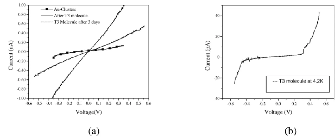
Fig. 6 shows the current voltage characteristics of a device with gold clusters before and after insertion of T3 in the tunneling barrier. Dodecanethiol is replaced by introducing T3 molecules, which give rise to an increased current through the tunnel junctions. As we can see at 0.3V conductivity increases almost by a factor of two which is expected but not as high as it is observed in the case of in-plane dc measurement [6]. T3 molecule belongs to oligothienyl family, which has π-type molecular orbitals that gives higher mobility compare to σ-type orbitals [7]. In long molecules, π-orbitals are delocalized and can open a channel for electrons to pass through under bias. In fig. 6 (b), we can see a typical Coulomb blockade at 4.2K for our studied devices, with a 0.35V blockade voltage.
-0.6 -0.5 -0.4 -0.3 -0.2 -0.1 0.0 0.1 0.2 0.3 0.4 0.5 0.6 -1.00 -0.80 -0.60 -0.40 -0.20 0.00 0.20 0.40 0.60 0.80 1.00 Au-Clusters After T3 molecule T3 Molecule after 3 days
Cu rr en t ( n A) Voltage(V) -0.6 -0.4 -0.2 0.0 0.2 0.4 0.6 -40 -20 0 20 40 --- T3 molecule at 4.2K Cu rr en t ( p A) Voltage (V) (a) (b)
Fig. 6: (a) IV characteristics of thiol terminated Au-clusters and T3 molecule. (b) IV characteristics of thiol terminated Au-clusters and T3 molecule at 4.3K.
The strong temperature dependence and the shape of the Coulomb blockade indicate that the current flow goes through several gold clusters, which results in broader coulomb blockade at 4.2K which is in agreement with what is observed in Fig.5.
Another phenomena that we have observed is the evolution of conductivity of T3 molecule by time as shown in the fig.6(a). It can be seen from the plot that at 0.4V conductance increases roughly by one order of magnitude. We believe that long stabilization time of the T3 molecule in the system is the reason for time dependence of the conductance. Further investigation is under progress to explore this phenomenon.
Conclusion
We described two methods for fabricating electrodes with nanometer separation (1-5nm) and also a method for fabricating devices for TEM observation. The main objective of the work was to study transport properties of T3 molecules and its influence on conductivity of the alkanethiol terminated gold clusters. Moreover, our observation of increase of the conductivity with respect to time could be of interest for future investigation.
Acknowledgement
The author would like to acknowledge the financial support from the European Commission through its FET-NID program project NANOMOL.
References
1. Y.Tour et. al. IEEE, Proc. Of IEEE Vol. 85, No.4, P.486, 1997
2. Reed M A Molecular-scale electronics Proc. IEEE Vol. 87, No.4, April 1999, p. 652-658 3. S. H. Magnus Persson, Linda Olofsson, Linda Gunnarsson, A self-assembled single-electron
tunneling transistor, Appl. Phys. Lett. 74, 2546 (1999).
4. M.Brust, M.L. Walker, d. Bethel, D.J.Schriffin and R. Whyman, J. Chem. Soc. Chem.Commun., 801-802, 1994.
5. D.V.Leff, P.C. Ohara, J.R. Heath and W.M. Gelbart, J. Phys. Chem. 99, 7036-7041, 1995 6. Jean-Phillippe Bourgoin, Christophe Kergueris, Elisabeth Lafevre,, Serge Palacin, Thin solid
films, 327-329, 1998, 515-519
7. M.A. Ratner, and J. Jortner, Molecular electronics: Some directions, in Molecular electronics, Eds. London, U.K: Blackwell, 1997