Charge Transport in Nanopatterned PbS
Quantum Dot Arrays
by
Colloidal
Nirat Ray
M. Sc., Indian Institute of Technology, Delhi (2009)
Submitted to the Department of Physics
in partial fulfillment of the requirements for the degree of
Doctor of Philosophy
at the
MASSACHUSETTS INSTITUTE OF TECHNOLOGY
I
go C) wI U L<
Co o c7: -co
Q LL :: V) -j u)February 2015
@
Massachusetts Institute of Technology 2015. All rights reserved.
Author ...
Certified by ...
Signature redacted
-A
Department of Physics
September 24, 2014
S"I /1Signature redacted
Marc A. Kastner
Donner Professor of Science
Accepted by...
/
Thesis Supervisor
Signature redacted
V ~Krishna Rajagopal
Professor and Associate Department Head for Education
Charge Transport in Nanopatterned PbS Colloidal Quantum
Dot Arrays
by
Nirat Ray
Submitted to the Department of Physics on September 24, 2014, in partial fulfillment of the
requirements for the degree of Doctor of Philosophy
Abstract
In this thesis, we study charge transport in nanopatterned arrays of PbS colloidal quantum dots using conventional two-probe measurements and an integrated charge sensor. PbS dots are synthesized in solution with an organic ligand or cap that serves to passivate the surface of the dot, provide a tunnel barrier as well as colloidal stability. These dots can self assemble into an array as the solvent evaporates from a drop of solution on a surface. The self-assembled arrays can be thought of as tunable artificial solids, where the coupling between the dots can be tuned by changing the ligand.
Using electron beam lithography followed by a lift-off process, we develop a novel technique to nanopattern these arrays and present the first colloidal quantum dot ar-rays of nanoscale dimensions. Nanopatterning makes it possible to study the electrical properties intrinsic to the dots unimpeded by macroscopic defects, such as cracking and clustering that typically exist in larger-scale arrays. We find that the electrical conductivity of the nanoscale films is higher than that of drop-cast, microscopic films made of the same type of dot. We achieve unprecedented versatility in integrating the patterned films into device structures, which will be valuable both for studying the intrinsic electrical properties of the dots and for nanoscale optoelectronic applications. From two-probe measurements on the nanopatterned arrays that are approximately 15 dots wide, we observe large noise in the current as a function of time. The noise is proportional to the current when the latter is varied by applying source-drain or gate voltage in a field-effect structure or when changing temperature. Owing to the small number of current paths in the system, we often observe telegraph switching, and find that the off times follow non-poissonian statistics. We show that the results can be understood in terms of a model in which a quasi-one-dimensional percolation path is turned on and off, by charging of a dot along the path.
Long organic ligands lead to highly resistive colloidal quantum dot arrays, making the low bias regime inaccessible with conventional two-probe measurements. We use an integrated charge sensor to study transport in the low bias regime as a function of the coupling between the dots. We present transport measurements on butylamine
and oleic acid capped PbS dots. The resistances measured are the highest measured for colloidal quantum dots. For the native oleic acid ligand, and weak coupling between the dots, the conduction mechanism is nearest neighbor hopping, and the conductance is simply activated. At low source-drain bias voltages, the activation energy is given by the energy required to release a carrier from a trap state plus the activation over barriers resulting from site disorder. The barriers from site disorder are eliminated with a sufficiently high source-drain bias. For the shorter ligand, which gives stronger coupling, the data are consistent with Mott's variable range hopping as the conduction mechanism.
Thesis Supervisor: Marc A. Kastner Title: Donner Professor of Science
Acknowledgments
You know you've reached the end of the long road called 'Ph.D.' when eventually the time comes to write the acknowledgements. The Kastner group has been home to me for the last five years, and it is not without a certain degree of nostalgia that I prepare to hand in my dissertation. I want to take this opportunity to acknowledge all the people who contributed positively to my graduate school experience.
First and foremost, I thank my advisor, Marc Kastner, for accepting me into his group and guiding me at every step. Marc's enthusiasm and unwavering support has been the greatest source of inspiration for me. I admire his deep and intuitive understanding of physics, his unlimited patience, and the faith he has in his students. His mind is like a steel trap and the solution to whatever problem I was facing was, more often than not, something he had read about or experienced years ago. I have particularly enjoyed the last six months that he spent in his building 13 office.
Moungi Bawendi, while not formally an advisor, welcomed me to his group meet-ings, invited me to present my work, and met me individually to discuss research. I appreciate his deep and sincere value of quality science, and his simultaneous interest in the product market.
I have had the good fortune to work with many talented and fun students and post-docs throughout my time as a graduate student. Kenny MacLean warmly greeted me when I first joined the lab, and was happy to share his knowledge and experience. In the short overlap that we had, he was a fun officemate, and I really enjoyed discussing science and life outside the lab with him. I worked closely with Tamar Mentzel on nanopatterning colloidal quantum dot arrays and part of the noise measurements. I appreciate her enthusiasm, resourcefulness and her extraordinary ability to sell her research. Neal Staley joined our group as a postdoc when I was a third year graduate student. I really enjoyed discussing data with Neal, because he always has good ideas and suggestions for further experiments. He left his office door open for me to barge in with questions, especially while he ate lunch. I am grateful to him for forcing me to think about the story behind data, and appreciate the ingenuity and commitment
he brings to his work. I enjoyed getting to know Jingshi Hu, Colin Dillard, Xi Lin and Andrew Lai.
In the Bawendi group, I worked closely with Darcy Wanger. Darcy has been a joy to work with and I appreciate her integrity and diligence in research. I would also like to thank other people from Moungi's group: Jennifer Scherer, who has been my go to person after Darcy graduated, Gyuweon Hwang (Q1) for making sure the glovebox was in perfect condition and Dorthe for teaching me how to give a good presentation. The fabrication part for this thesis was done in MITs Microsystems Technology Lab (MTL) and the Scanning electron beam laboratory (SEBL). I would like to thank Vicky Diadiuk and Judy Hoyt for their help and guidance with fabrication. I thank Paul Tierney, Eric Lim, Bernard Alamariu, Paudely Zamora, Bob Bicchieri, Scott Poesse and Dan Adams, not only for training me and helping me in the clean room, but also for being friendly faces (behind the bunny suits). One of the best learning experiences for me has been during the year when I served as a student member of the Process Technology committee (PTC). The nanopatterning aspect of this work would not have been possible without the expert guidance of Mark Mondol. I admire his patience and dedication, as he sat with me for extended periods of time while we perfected the alignment process.
The International Fulbright Science and Technology program and the U.S. De-partment of State, generously provided my graduate fellowship for the first three years of graduate school. I appreciated the creative and intellectually stimulating gatherings that they organized every year. The last two years of my graduate school were funded by the Schlumberger foundation Faculty for Future fellowship aimed at encouraging women in physics.
While at MIT, I have benefited greatly from the camaraderie and friendship, and many times good food, from the MIT Women in Physics and the the Graduate Women at MIT (GWAMIT). Anne White has been my my faculty mentor for almost two years now. She helped me through some rough patches and I have really enjoyed our long discussions over coffee.
faculty who care a great deal about students and research. I really enjoyed the courses taught by Wolfgang Ketterle, Mehran Kardar and Patrick Lee. I am grateful to many staff members at MIT, who helped make life easier at every turn. They include Monica Wolf, Catherine Modica, Jacqueline Carota, Crystal Young, Katie Lewis, Ting Ting Li, Anita Caputo, Annie Lee, Ed Kruzel and Rebecca Maitland.
Much of my initial time at MIT was spent doing problem sets and studying for general exams. I would like to thank Mackenzie Van Camp, Dillon Gardener, Patrick Brown, Laura Popa, Duncan Ralph, and Javier Sanchez-Yamagishi, without whose assistance these times would have been much more difficult, and much less fun.
I must thank my family and my extended family, for their support and encour-agement. They may not have had a clue about what I was doing for the last five years, but they were constantly telling me I could do it. Finally, I thank my beloved husband, partner and friend, Guru Saran Mishra, for his constant love and support. None of this would have been possible without him.
Contents
1 Introduction 25
1.1 Colloidal quantum dots . . . . 27
1.1.1 Optical properties . . . . 29
1.1.2 PbS quantum dots . . . . 31
1.2 Quantum dot arrays and superlattices . . . . 32
1.2.1 Binary superlattices . . . . 34
1.3 Electronic coupling and charge transport in quantum dot arrays . . . 36
1.4 From fundamentals to device applications . . . . 39
1.5 Thesis overview . . . . 40
2 Synthesis, nanopatterning and characterization of PbS colloidal quan-tum dots 43 2.1 Chemical Synthesis of Colloidal quantum dots . . . . 43
2.1.1 Synthesis of PbS dots . . . . 45
2.2 Need for nanopatterning . . . . 47
2.3 Overview of existing patterning techniques . . . . 48
2.4 Nanopatterning colloidal quantum dots . . . . 50
2.5 Ligand exchange . . . . 55
2.6 Film morphology and characterization . . . . 57
2.7 Electrical properties . . . . 62
3 Noise in nanopatterned colloidal quantum dot arrays 65 3.1 Noise and fluctuations in solids . . . . 65
3.2 Noise in disordered and inhomogeneous systems . . . . 70
3.2.1 Overview of noise in colloidal quantum dots . . . . 73
3.3 Device Fabrication . . . . 74
3.4 Instrum entation . . . . 75
3.5 R esults . . . . 76
3.5.1 Bias and gate voltage dependence . . . . 76
3.5.2 Temperature dependence of noise . . . . 82
3.5.3 Effect of changing the ligand . . . . 83
3.5.4 Hysteresis and memory effects . . . . 87
3.6 D iscussion . . . . 90
4 Charge sensing in PbS colloidal quantum dots 95 4.1 Measuring transport in colloidal quantum dot arrays . . . . 96
4.2 Conductance measurements using charge sensing . . . . 98
4.2.1 Diffusion M odel . . . 103
4.2.2 Limits of measurement technique . . . 104
4.3 Transport in butylamine capped PbS quantum dot array . . . 106
4.3.1 Electric field dependence . . . . 110
4.3.2 Gate voltage dependence . . . . 114
4.4 Transport in Oleic acid capped PbS quantum dot arrays . . . 116
4.5 D iscussion . . . 120
4.6 Sensing fluctuations with a charge sensor . . . 125
4.6.1 Dual MOSFET charge sensing . . . . 126
5 Conclusions and Future work 129 A MOSFET Fabrication 135 B Electron Beam Lithography 141 B.1 Electron beam lithography using Elionix-ELS125 . . . . 141
List of Figures
1-1 (a) Cartoon of a colloidal quantum dot. (b) High resolution Transmis-sion electron micrograph of a PbSe dot showing the crystal structure
of the dot. Image taken by Darcy Wanger from Bawendi group. . . . 27 1-2 Schematic of (a) density of states for a bulk semiconductor as compared
to a semiconductor quantum dot. Starting from a continuum of density of states in the bulk, as the size of the dot decreases, the separation between energy levels increases. The increase is more dramatic near the band edge, and the states at the center of the band may still be considered to be continuous. (b) absorption spectrum of a bulk semiconductor (black dashed line) compared to that of a semiconductor quantum dot. The absorption spectrum of a bulk semiconductor is continuous, but in a dot it consists of a series of discrete transitions
with very high absorption intensity at the transition frequencies. . . . 30
1-3 (a) From colloidal dots to arrays. A small volume of the colloidal dispersion is dropcast onto a surface, and the solvent is allowed to slowly evaporate. The rate of solvent evaporation coupled with the inter-dot forces determines the ordering length scale in the system, leading to the formation of a two or three dimensional 'artificial solid'. (b) Unlike classical solids, artificial solids are tunable. We can tune the energy levels of each dot by changing the size of the dot. We can tune the inter-dot coupling by modifying the height and width of the tunnel barrier, Ax, by changing the ligand or capping molecule attached to
1-4 Transmission electron micrograph and model of a binary nanoparticle superlattice (BNSL) self-assembled from core-shell 4 nm and 8 nm PbS/CdS and CdSe/ZnS quantum dots. Image taken by Gyuweon Hwang from the Bawendi group. . . . . 35
1-5 (a) A phase diagram showing the different coupling regimes expected for a quantum dot array with size and/or packing disorder. The ver-tical axis is a measure of the disorder energy, and the x-axis is the di-mensionless parameter Ec/(Ec +
$),
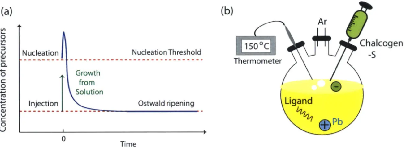
where E, and 3 are the Coulomb charging energy and the inter-dot coupling energy, respectively. For large disorder, weak electronic coupling can lead to Anderson local-ization. Reducing the disorder allows for the inter-particle couplings. At very small disorder, Coulomb effects dominate with a Mott-like transition from a delocalized to a site-localized state. Figure adapted from [92]. (b) Colloidal dots can self assemble into ordered 3D closely packed colloidal crystals, with the structure of stacked 2D triangular lattices, as shown in the transmission electron micrograph of PbS dots. Collective or commensurate charge ground states have been predicted to form in these triangular arrays for special densities such as 1 elec-tron for every 3 dots [83], as shown sketched over the TEM image of a PbS quantum dot array. Blue circles depict an electron and white lines highlight the underlying array structure. . . . . 372-1 (a) Sketch depicting the nucleation and growth phases in the synthesis of monodisperse colloidal quantum dots. (b) Cartoon of the apparatus
2-2 Transmission electron micrographs of PbS dots. (a) Freshly prepared butylamine capped PbS dots. (b) If we expose the dots to elevated temperatures (even 5-10 degrees above room temperature) after the growth step is complete, Ostwald ripening takes place. Briefly, Ostwald ripening is when atoms from the surface of smaller dots (with high surface energy) leave to join the surface of larger (lower surface energy) dots, giving a broad distribution of dot sizes. . . . . 46 2-3 (a) Schematic of colloidal dots drop cast on an inverted FET device
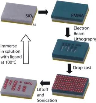
(side view). (b) Scanning electron micrograph of a PbSe film drop cast on an inverted FET device (top view; the gold electrodes, which are beneath the film and thus obscured from view, are outlined in orange), and (c) after annealing the film for one hour at 400 K. (d) When the thickness of the film exceeds approximately 1 pum, cracks emerge as the film dries. Image also appears in [69]. . . . . 48 2-4 An overview of the process for patterning nanoscale films of colloidal
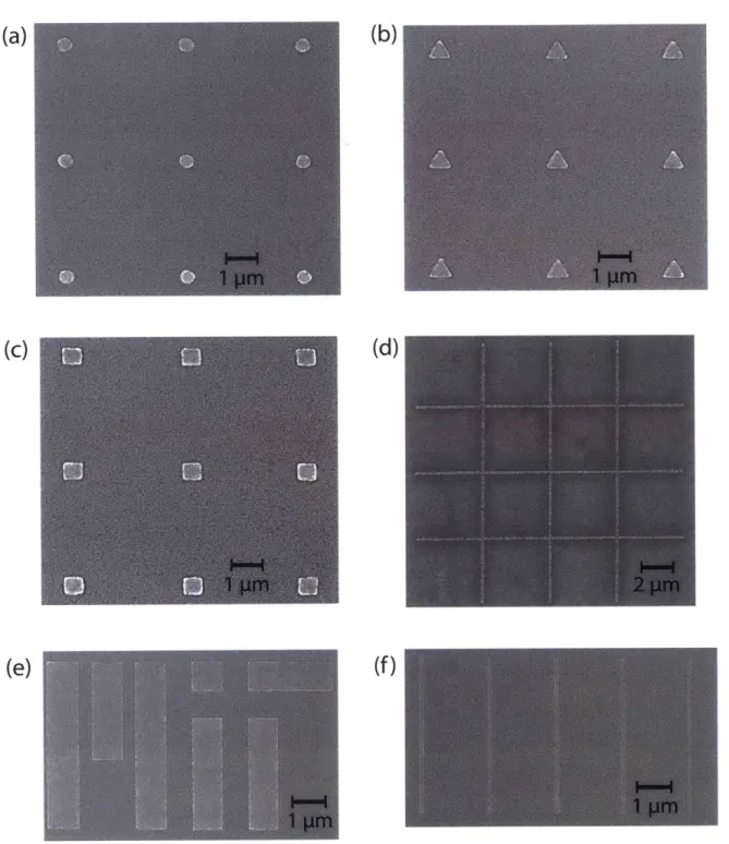
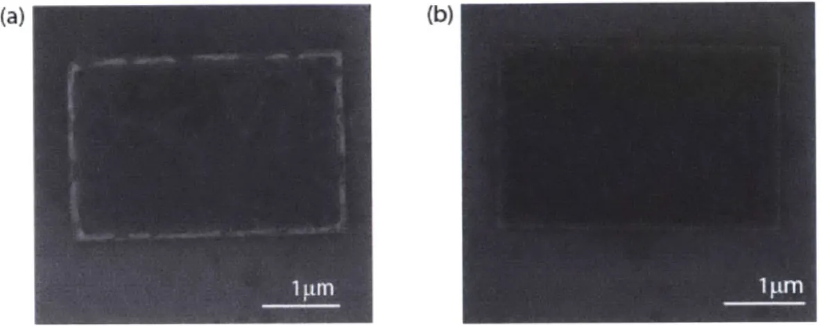
d ots. . . . . 50 2-5 Scanning electron micrographs (a)-(f) of nanopatterned films of oleic
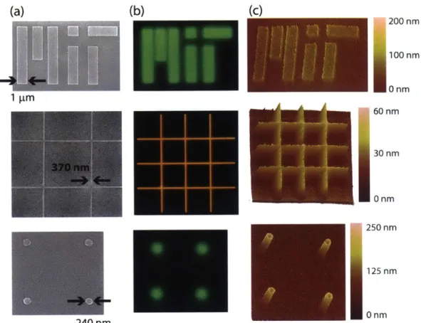
acid capped PbS quantum dots. . . . . 52 2-6 Nanopatterned films of CdSe quantum dots (first and third rows) and
ZnO.5Cdo.5SeZno.5Cdo.5S coreshell dots (second row). (a) Scanning
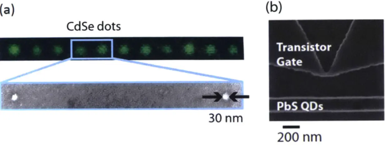
elec-tron micrograph, (b) fluorescence (actual color), and (c) AFM images. Image also appears in [69]. . . . . 53 2-7 (a) Fluorescence and Scanning electron microscope (SEM) image of
30 nm small patterns of ZnO.5CdO.5SeZnO.5CdO.5S coreshell dots with
a phosphonic acid ligand (b) 200 nm wide pattern of PbS dots with butylamine ligand, placed 200 nm away from a transistor gate. . . . . 54 2-8 Scanning electron microscope (SEM) images of PbS films with post
de-position ligand exchange from butylamine (BA) to the shorter ethanedithiol (EDT) ligand. (a) Ligand exchange performed before lift off, and (b) ligand exchange performed after lift-off. . . . . 56
2-9 Atomic Force Microscope (AFM) images and line scans of patterns with butylamine capped PbS dots. (a) 400 nm wide circles created with 200 nm resist, (b) 200 nm wide lines created in 200 nm resist, and (c) 600 nm wide rectangular pattern on 60 nm thick Ti/Au electrodes created on 200 nm thick resist . . . . 58
2-10 Transmission electron micrographs showing the formation of patterned films. (a) Patterns made on SiO2 TEM grids showing formation of film
starting at the edge of the resist. (b) As the dropcasting solution is made more concentrated, complete coverage of the pattern is achieved. (c) Packing of butylamine capped PbS dots in the middle of the pattern showing a close packed film. (d) Packing of oleic acid capped PbS dots
from the middle of the pattern showing polycrystalline structure. . . . 61
2-11 Helium ion microscope images of patterns formed after treatment of the oxide with 0.2 M (3-mercaptopropyl)trimethoxysilane (MPTMS, in toluene). . . . . 62
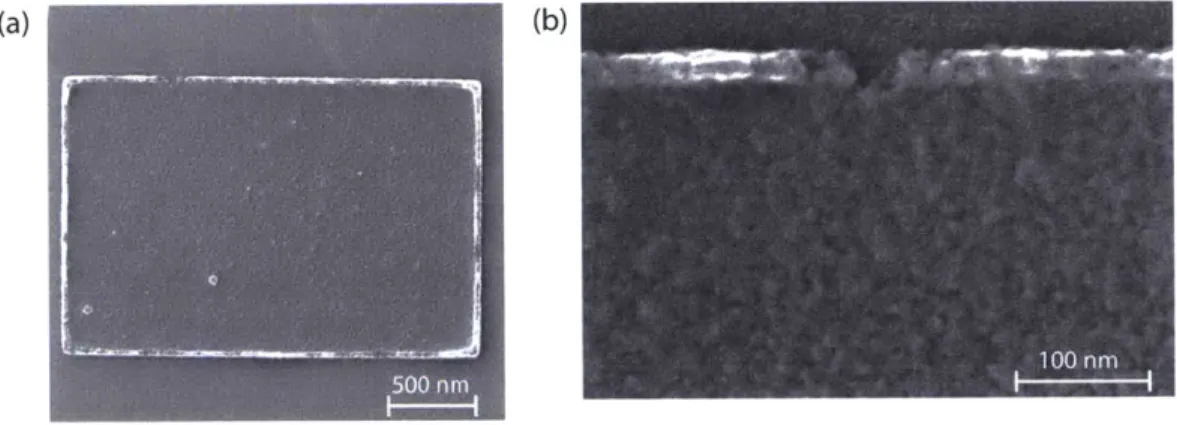
2-12 (a) An AFM image of a film of butylamine capped PbS dots, which is 350 nm wide at its narrowest point. The film is continuous, in contrast to those shown in Figure 2-3 (b)-(d). (b) Current-voltage characteristic of the nanopatterned film shown in (a). (c) Conductance of butylamine
capped PbS dots versus the dimensions of the film with Vd, = 0.1 V. The red circles represent the conductance of the nanopatterned film shown in (a) and a comparable rectangular film with nanometer dimensions. The blue circles represent the conductance of unpatterned films in a device structure shown in Figure 2-3. The conductivity of the nanoscopic films is 180 times higher than what is found in the microscopic films. Image also appears in
[69].
. . . . 633-1 (a) Random telegraph noise (RTN) observed in a silicon MOSFET. The current from the device jumps between an on and an off state. The origin of telegraph noise in a MOSFET is the capture and release of single electrons from a trap state, probably in the oxide. (b) The probability distribution of the on time, P(tn) and (c) off time P(toff) obtained from telegraph noise measurements. The green and red lines are fits to the functional form given by equation 3.4 . . . . 70
3-2 The random resistor network (bond percolation) (a) Thick blue lines and black dashed lines correspond to unbroken and broken bonds re-spectively. 1 shows an isolated cluster, 2 shows a dead end, and 3 shows a segment of the infinite cluster backbone. (b) A 3 x 3 network with a conducting path between the electrodes. As an external bias is applied, V > Vth, a new conduction channel opens up between points
4 and 5. ... .
... .. ... ... . .. . .. ... ..72
3-3 Schematic of a typical device structure for two probe transport and noise measurements on nanopatterned colloidal quantum dots. For measurements on nanopatterned arrays of dots, gold electrodes are patterned with electron beam lithography. The dots are placed only in the area between the electrodes. . . . . 74
3-4 (a) Optical microscope image and (b) false color scanning electron micrograph of patterned gold electrodes and 80 nm wide butylamine
3-5 Current-Voltage (I-V) characteristics of nanopatterned PbS dots. (a) I-V curves for 80 nm wide pattern showing excess noise in the current. Inset shows noise in the current in the time domain at a source drain bias of 23.2 V. (b) Histogram of the current measured as a function of time for different values of the source drain bias, as indicated in the figure. The dashed lines in the histograms are Gaussian fits. The current noise, AI, is given by the full width at half maximum from the fits. (c) Log-log plot of the current noise, Al, extracted from the histograms, as function of the average current, I. We see the the excess noise is proportional to the average current. The black dashed line denotes the noise floor of our circuit, and the red dashed line is a linear fit to the data above the noise floor. . . . . 77 3-6 (a) Power spectral density of current noise, Si, in units of A2/Hz as
a function of increasing source-drain bias, showing 1/f noise below 10 Hz. The magnitude of 1/f noise increases with increasing source-drain bias. (b)-(e) show I-V measurements on nominally identical 80 nm wide butylamine capped PbS nanopatterns. While the dimensions of the nanopatterns are the same, (b) and (c) are made on 100 nm thick SiO2, whereas (d) and (e) are made on 300 nm of SiO2. The
differential conductance ranges from 10 1 2Q-1 for (b), to immeasurably small (>10-1 4
Q-1) for a significant number of devices . . . . 79
3-7 (a) Noise as a function of gate voltage at room temperature. As seen from the current-voltage characteristics, the noise increases with in-creasing gate voltage (Vg), but this can be seen clearly only when the applied gate voltage is larger than the source-drain bias. (b) Percentage
fluctuation in the current, for different pattern widths, with constant
electrode spacing. Multiple data points for a single width represent the sample to sample variation. The line serves as a guide to the eye to show that the noise scales inversely with the width of the pattern. 81
3-8 Histograms of the current at fixed source-drain bias, Vd, = 25 V, as function of temperature for 80 nm wide butylamine capped PbS nanopatterns. . . . . 83
3-9 (a) Current-voltage characteristics of 200 nm wide butylamine-capped PbS nanopatterns for different temperatures. (b) Average current, I,, (black squares), and current noise, Al (filled red squares), at VdS = 15
V as a function of 1000/T, where T is the temperature. The current noise, AI, follows the average current just as one would expect for conductance fluctuations. The lines serve as guide to the eye . . . . . 84
3-10 Current-voltage characteristics for 200 nm wide nanopatterns of oleic acid capped PbS dots. Note the telegraph nature of the noise. . . . . 85
3-11 (a) Current measured as function of time at different temperatures, for 200 nm wide nanopatterns of oleic acid capped PbS dots. (b) Tele-graph events are most clearly observed at temperatures below room temperature, and the switching rate decreases with extended measur-ing time. Top and bottom traces show switchmeasur-ing events on the first and third day of measurement. The average current is subtracted from all of the time traces for ease of comparison. (c) Histograms of the off
times on a log-log plot fit well to a power law, p(toff) = A/t j+', with
= 0 .6 . . . . 8 6
3-12 (a) Hysteresis in current-voltage characteristics of oleic acid capped dots. Red solid lines depict the current as the source-drain bias is raised from 0 to 16 V. We hold the voltage at 16 V for 1 hour and turn the source-drain bias down to 0 V again. Black dashed lines denote the current measured during the sweep down. (b) Current as a function of time for different temperatures, immediately after sweeping the source-drain bias up to 16 V. . . . . 88
3-13 Memory effects: (a) Current as the voltage is swept from 0 to 8 V for a 200 nm wide pattern of butylamine capped dots. The red trace is the first sweep up to 8 V. We then measure the current as a function of time for 10 minutes (plotted red in (b), and then sweep the voltage down. The sweep down, not shown in the figure, coincides exactly with the blue trace. The blue curve is the second sweep up to 8 V. Once again we measure the current as function of time (plotted black in (b), and then sweep the source-drain bias back to 0 V. The sweep down and subsequent sweep up are represented by the black trace. (b) Current as a function of time. The red time trace shows the current as a function of time after the first voltage sweep. The current decays from 7 pA to I1 - 6 pA in 500 seconds. During the next voltage sweep, the system remembers that the current had dropped to I1, and we observe a decay to a lower value I2 - 5.5 pA in 500 seconds. . . . . 90
3-14 (a) Current-voltage characteristics at room temperature, before (black dashed line), and after (red line), heating the sample to 303 K. (b) Current as a function of time for Vd, = 15 V. The red shaded region indicates changing temperature. . . . . 91
4-1 (a) Schematic , and (b) optical micrograph of a narrow channel sili-con MOSFET. The device sili-consists of an n-channel silisili-con MOSFET positioned approximately 100 nm away from a nanopatterned array of dots. The gate of the MOSFET tapers to a width of 80 nm wide at its narrowest point and a positive voltage on the top gate induces an inversion channel of a comparable width at the Si-SiO2 interface. (c)
Schematic illustrating the band bending in a n-channel MOSFET for the formation of an inversion region. (d) Conductance of the inversion region, Gm measured with 32 pV ac excitation as a function of voltage applied to the top gate, at 295 K (red) and 4 K (blue). . . . . 99
4-2 (a) False colored scanning electron micrograph of butylamine capped PbS nanopattern (red), adjacent to a narrow channel MOSFET gate (blue). The nanopattern is connected to one of the gold electrodes, but is 100 nm away from the other one. This geometry helps us to distinguish the response of the MOSFET to charge being added to the nanopattern and the gold electrodes. (b) Measurement technique (T = 40 K). The upper panel shows the voltage pulse applied to the gold electrodes as a function of time. The lower panel shows the response of the MOSFET, GM, on pulsing the electrode connected to the nanopat-tern (black) and the the response on pulsing the electrode disconnected from the nanopattern (blue), at T = 40 K. The observation confirms a transient response caused by slow charging of the resistive nanopattern. 101
4-3 Device and circuit used for charge sensing measurements. The resistive material, is modeled as a distributed RC network. A key assumption for the formalism, is a uniformly distributed resistance over the length scale. . . . . 102
4-4 Screening and limits of measurement (a) The top trace (red line) shows the voltage step applied to the gold contact at T = 4 K. The lower trace shows the slow recovery of the MOSFET conductance, as discussed in the main text. (b) Screening rate, r, extracted from exponential fit to the recovery, as a function of inverse temperature for low temperatures. (c) Change in screening rate Ar = r - rmin as a function of inverse temperature. The solid line is a theoretical fit described in the main text. (d) Screening from other sources at higher temperatures give slower recovery at high temperatures. . . . . 105
4-5 (a) False color scanning electron micrograph of a 200 nm wide nanopat-tern of butylamine capped PbS dots (red), connected to gold electrodes placed a micron apart. The nanopattern and the gold electrodes are defined with electron beam lithography and placed 100 nm away from the narrowest part of the Al gate of the MOSFET. (b) Current-voltage characteristics of the nanopattern from room temperature to 100 K. (c) Conductance of the MOSFET, GM, as a function of time as the voltage on one of the gold electrodes is stepped from 0 to -1 and back to 0 at 80 K, and (d) 28 K. . . . . 107
4-6 (a)Conductance of the butylamine capped PbS dot array, Gpbs, as a function of temperature, obtained from charge sensing (open circles) and current measurements (filled circles), measured at a source drain bias of 0.5 V. The black dashed lines are theoretical fits to simply
activated transport with two activation energies as described in the main text. (b) Conductance, Gpbs, plotted as a function of 1/T1/4.
Black dashed line is a fit to Mott's variable range hopping. . . . . 110
4-7 (a) Differential conductance, gpbs, of butylamine-capped PbS dots as a function of applied field across the dots, for different temperatures (b) Temperature dependence of the differential conductance of buty-lamine capped PbS dots for different fields (c) Variable range hopping distances, rm, extracted from exponential fits to the field dependence of the differential conductance, dI/dV, where the current, I, is described by equation 4.5. (d) Activation energies extracted by fitting the con-ductance to a sum of two simply activated processes. . . . . 112
4-8 Gate voltage dependence for butylamine capped PbS dots (a) Current-voltage characteristics for different gate Current-voltages at 100 K. V9 = OV for black circles, Vg = -5 V for filled orange circles, V9 = -7 V for green triangles and V9 = -10 V for filled blue circles. Inset shows the
differential conductance at around 5 V source drain bias as a function of gate voltage at 100 K. (b) Current as a function of gate voltage and temperature at source drain bias of 5V. . . . . 115
4-9 Transport in oleic acid capped PbS dots (a) Asymmetry in current-voltage characteristics between positive and negative source-drain bias at lower temperatures. Inset shows the gate voltage dependence at 170 K, the current increases as a negative gate voltage is applied con-sistent with holes being the majority carriers. (b) Current-voltage characteristics as a function of temperature for positive source-drain bias. (c) The voltage on one of the gold electrodes connected to the nanopatterned array is stepped from 0 to -1. As charge diffuses in the distributed RC network of the array, the conductance of the MOSFET varies exponentially with time. Solid markers show the MOSFET con-ductance in response to the voltage pulse at 50 and 60K, for a source drain bias of 3.5 V. Solid black lines are fits to G = Goexp(-Ft) where F = 72 gPbs-OA/wLC and gPbs-oA is the differential conductance per
square of the nanopatterned oleic acid capped PbS array at 3.5 V. (d)
gPbs-oA at Vds = 3.5 V, as a function of inverse temperature. Open circles represent differential conductance extracted from charge sensing measurements and filled circles are the data extracted from measuring the current. . . . . 117
4-10 (a) Differential conductance of oleic acid capped PbS dots, gPbs-oA, as
a function of inverse temperature, for different values of electric field or bias voltages across the dot array. Filled markers represent differential conductances extracted from the current-voltage characteristics, and empty markers represent the differential conductances extracted from charge sensing measurements. Black dashed lines are fits to gPbs-oA
~ exp(-Ea/kBT), where E is the activation energy. (b) Activation energy, Ea, as a function of the applied electric field. Blue markers indicate the data points and the black dashed lines represent straight line fits to the data. We extrapolate the straight line fit at low fields to zero bias, in order to estimate the activation energy near zero bias. 119
4-11 (a) and (b) illustrate the two components of the activation energy and the associated length scales. At high field, length scales for the low and high field conductance. 'd' is the inter-dot distance, and 'x' is the separation between the surface of the dot and an adjacent dot. . . . . 121
4-12 (a) Sample to sample variation. Conductance of nanopatterned buty-lamine capped PbS dots, GPbS-BA, as a function of inverse temper-ature, for two nominally identical samples, at a source-drain bias of 0.5 V. As before, filled markers represent current measurements and empty markers represent transient measurements. (b) Differential con-ductance, g, at a bias of 14.5 V, measured from current measurements for butylamine capped nanopatterns (green markers), and oleic acid capped nanopatterns (blue markers), as a function of inverse temper-ature. We observe that while the resistance of these two samples is
comparable at the given field, the temperature dependence is remark-able different. . . . . 122
4-13 Noise correlations measured at 230 K (a)Current, IPbS-OA, at a bias of 8V, as a function of time from oleic acid capped PbS dots, showing clear telegraph noise. (b) Correlation, c(T) between the current, IPbS-OA and
Gm calculated from data such as that shown in (a), as discussed in the
m ain text. . . . . 125
4-14 Dual MOSFET charge sensing (a) False colored Scanning electron mi-crograph of two MOSFET gates, placed 200 nm apart. (b) False col-ored scanning electron micrograph of a nanopatterned PbS array placed 50 nm away from each sensor. The alignment procedure to achieve this configuration is discussed in Appendix B. (c) Conductance of both MOSFETs in (a), measured with a DC bias, as a function of time. The upper and lower panels show conductance of the top and the bottom MOSFET respectively. Telegraph events in each trace originate from electron trapping and de-trapping in the nearby oxide. (d) Correlation analysis between the MOSFET conductances, shows no peaks, con-firming that the sensor noise in each of the MOSFETs is uncorrelated. 128
5-1 Applications of charge sensing to study transport. We plot the resis-tance of the material under study as a function of the observed/expected
contact resistance. Our technique can be used to probe transport for materials above the black dashed line; highly resistive materials, which may have a high contact resistance. . . . . 132
B-i Layout file for charge sensor adjacent to the nanopattern. The top left box, shows the optical alignment markers (red), Al and A2, used for
patterning the gold electrodes, and the e-beam alignment markers, BI and B2 (golden), used for the MOSFET gate alignment. Note that both these sets of alignment markers are separated in Y, but have the same X-coordinate. Gray boxes show how the edges of the 600 pm write-fields. The top right design, is a zoom in of the area in the blue box and reveals the markers (golden), C1-C4, used for four-point alignment of the MOSFET gate. Further magnification of the design, reveals the alignment markers used for positioning the nanopattern (Dl-D4, bottom right), and the optical and e-beam alignment markers (bottom left). . . . . 142 B-2 Scanning electron micrographs of the Ti/Au e-beam electron mark Bi
using the Elionix system. The image on the right is the magnified version of the area in the black box from the left image. . . . . 143
Chapter 1
Introduction
Low-dimensional nanometer-sized systems have defined new research areas in con-densed matter physics. When electrons and holes are confined by potential barriers to small regions of space where the dimensions of the confinement are less than the de Broglie wavelength of these charge carriers, pronounced quantization effects develop. The length scale below which strong quantization effects begin to occur ranges from about 5 nm to 25 nm for typical semiconductors. The confinement can take place in one dimension, giving quantum wells, in two dimensions, giving quantum wires, or in all three dimensions, giving quantum dots.
A system of electrons confined in all three dimensions has discrete energy and charge states, just like atoms and molecules, and for this reason quantum dots are also known as artificial atoms. As a simple example, we can think about the particle in a box problem, of a particle free to move in a small space surrounded by impenetrable barriers. By solving the Schrodinger's equation, we get quantized energy levels, and wavefunctions which depend on the details of the confining potential. For a square box of side L with the potential V equal to zero inside the box and infinite outside,
the energy levels are given by n2 r2h2/2m*L 2, where, m* is the effective mass of the particle, and n is a quantum number. In order to observe energy quantization effects in a dot, the thermal energy (kBT) must be lower than the internal excitation energy, or the level spacing between the quantized energy levels. For a 10 nm box, the energy level spacing is of the order of an meV, and so to see quantization effects one needs
to go to temperatures below 10 K.
An isolated quantum dot also has a set of well-defined charge states, where each successive charge state corresponds to the addition of one more electron to the dot. Because of the coulomb repulsion between electrons, the energy difference between successive charge states can be very large, and this is given by the charging energy. The charging energy, Ec, can be described by simple electrostatics and is given by e2/2C, where, e is the electron charge, and C is the total electrostatic capacitance
of the dot.The charging energy depends on both the size of the dot and the local electrostatic environment. In general, the charging energy must be calculated for the specific geometry. For an isolated sphere of radius r, and dielectric constant c, the charging energy is given by E, = e2/87rEoEr. To observe charge quantization effects,
the charging energy must be larger than the thermal energy. For a spherical dot of diameter 10 nm, and dielectric constant of unity, the charging energy comes out to be 0.2 eV. This exceeds kBT = 26 meV at room temperature, indicating that thermal fluctuations in the charge of the dot will be suppressed. Charging effects are also destroyed if the tunneling rate between the dot and the electrodes is too rapid. Simple estimations from the uncertainty principle show that for resistances below h/e2, where h is the Planck's constant and e the electron charge, quantum
fluctuations smear out charging effects.
Broadly speaking, quantum dots can be fabricated in two ways. There are epi-taxial quantum dots that are defined by electrostatic gates on substrates, or that self-assemble on surfaces. In the most common approach to form epitaxial dots, we start with a GaAs/AlGaAs heterostructure, in which a 2DEG forms a distance below the surface. The 2DEG is then patterned to form isolated islands, either by etch-ing through the 2DEG, or by electrostatic patternetch-ing metal gates on the substrate surface. For the work presented in this thesis, we work with colloidal quantum dots fabricated using 'wet' methods which provide excellent control over size and shape.
(a) Core: Shell: Semiconductor Protective or 1-20 nm complementary 01- tf. Functional group: Chemically, electrically or optically active group
Ligand or Capping group:
Passivate and protect the surface
Figure 1-1: (a) Cartoon of a colloidal quantum dot. (b) High resolution Transmission electron micrograph of a PbSe dot showing the crystal structure of the dot. Image taken by Darcy Wanger from Bawendi group.
1.1
Colloidal quantum dots
A single colloidal quantum dot consists of a semiconducting or metallic core with a di-ameter of a few nanometers, capped by an organic material, or ligand, which serves to passivate the surface of the sphere, and to insulate the dot from its surroundings. The dot may contain a thin complementary shell of another material or other chemically, electrically or optically active groups. Figures 1-1(a) and (b) show a cartoon of a colloidal quantum dot, along with a high resolution transmission electron micrograph of a PbSe colloidal dot.
The core of a colloidal dot may be metallic (such as Al, Au, Fe), or semiconduct-ing (such as CdS, PbSe, PbS). For metallic dots, the spacsemiconduct-ing between energy levels depends on the Fermi energy of the metal, EF, and on the number of electrons, N, as:
Ac = 1/D(EF) = 4EF/3N (1.1)
For Au with a work-function of 5.5 eV, a dot with a radius of 2 nm has level spacing of the order of 2 meV, requiring sub-kelvin temperatures for measurement of internal excitation energies. The small level spacing compared to the large charging energy resulting from the small dot size, implies that the addition of electrons in metallic
dots is dominated by the charging energy. A semiconducting dot can be described, to a very good approximation, by a particle in a spherical box. For a spherical well with zero potential inside the box (r < R) and infinite outside, the Hamiltonian gives
eigenergies as:
En,i,m = En,1 = ' (1.2)
2m*R2
where, m* is the effective mass of the particle, and R is the radius of the box. The
coefficient 3
n,1 is the nth zero of the 1th spherical Bessel function. The quantum
numbers n, 1 and m are the same as used in the atomic notation of states, for example, n = 0, 1 = 0 would be the 1S state. For a CdSe dot ( m* = 0.13 me), with a radius of 2 nm the estimated spacing between energy levels (1S and IP) is approximately 1 eV, making it possible to observe quantization effects even at room temperature.
The most common ligand coatings described in literature are based on organic hydrocarbon molecules. The ligands used for synthesis typically have a small head group (such as a carboxylic acid) that has a high affinity for the dot surface, and a long tail to provide sterical stabilization in solution. Bulky organic ligands with long tails act as highly insulating barriers between dots, hindering charge transport. The complete removal of organic surface ligands has proven to be very difficult, and can lead to dangling bonds on the surface as well as trap states
[51].
Therefore, a simple exchange of the original bulky ligands by smaller molecules is a widely used approach for improving charge transport. While these lead to smaller tunnel barriers, they also lead to decreased colloidal stability of the dots, and is typically not performed in solution. The ligands can be exchanged to molecules with the same head group and a shorter tail, or to molecules with different head groups [104]. Cross-linking of dots using bi-functional ligands provides another approach to reduce the inter-particle separation, strengthen electronic coupling between dots, or attach them to electrodes or surfaces. The original long chain organic ligands can also be replaced by inorganic ligands such as soluble molecular metal chalcogenide complexes (MCCs). An attractive feature of MCCs is their facile thermal decomposition to metal chalcogenides, which not only further decreases the inter-dot spacing, but canalso create a layer of conductive 'glue' between the dots
[50].
It was recently shown that ligands can also provide an additional level of con-trol over the electronic properties [11]. The band energies of colloidal dots can be modified by ligand exchange, resulting in energy level shifts of up to 0.9 eV, as seen from ultraviolet photoelectron spectroscopy (UPS) measurements on PbS dots with different ligands. The trends in energy level position between different ligands have also been confirmed by atomistic modeling, showing that the observed shifts result from contributions from the dipole moment of the ligand as well as the dipole-surface
interaction.
Significant progress has also been achieved in the synthesis of core-shell quantum dots [104], obtained by growing a uniform layer of shell material around the colloidal dot. In the case of epitaxial semiconductor-semiconductor core-shell dots, the choice of materials for the core and the shell allows for controlling the confinement of elec-tron and hole wave functions, which, in turn, determines their optical and elecelec-tronic properties. The shell can serve to protect the core from oxidation.
1.1.1 Optical properties
For a semiconducting dot, both the electron states in the conduction band and the hole states in the valence band are quantized. Figure 1-2(a) shows a schematic of the density of states for a bulk semiconductor as compared to a semiconductor quantum dot. Starting from a continuum of density of states in the bulk, as the size of the dot decreases, the separation between energy levels increases, and it increases more dramatically near the band edge. The states near the center of the band are still close enough to be considered continuous. Quantization effects can be seen from the optical absorption or emission from colloidal dots, as the absorption/emission intensity becomes concentrated at specific frequencies corresponding to the transitions between discrete states. Figure 1-2(b) shows a schematic of the optical absorption from a bulk semiconductor (black dashed line) and from a semiconducting dot. The absorption spectrum of a bulk semiconductor is continuous, but in a dot it consists of a series of discrete transitions with very high absorption intensity at the transition
frequencies, and this has motivated researchers to create lasers
[6].
(a) Bulk Semiconductor (b)
Semiconductor Quantum dot
h he II 1P P -1 1D +1De e - - E hh CC E <
DOS DOS Eg Photon Energy
Figure 1-2: Schematic of (a) density of states for a bulk semiconductor as compared to a semiconductor quantum dot. Starting from a continuum of density of states in the bulk, as the size of the dot decreases, the separation between energy levels increases. The increase is more dramatic near the band edge, and the states at the center of the band may still be considered to be continuous. (b) absorption spectrum of a bulk semiconductor (black dashed line) compared to that of a semiconductor quantum dot. The absorption spectrum of a bulk semiconductor is continuous, but in a dot it consists of a series of discrete transitions with very high absorption intensity at the transition frequencies.
From studying optical properties of these dots, one can differentiate between weak and strong confinement regimes [24] by comparing the Bohr exciton radius, aB, given by h26/kte2, where p is the exciton reduced mass and c is the dielectric constant
of the semiconductor, with the dot radius, r. When the dot radius is much larger than the exciton radius, then the binding energy of the exciton is much larger than the quantization energy of both electrons and holes. The optical spectra is then determined by the exciton center of mass. This regime is the weak confinement regime (r>>aB). When the dot radius becomes much smaller than the exciton radius
(r<<aB), the optical spectra can be considered as transitions between electron and
hole levels as shown in Figure 1-2(b). Given the small exciton radius of ~10 nm in typical semiconductors, it not easy to achieve the strong confinement limit. However, quantum dots of lead salts (PbS, PbSe, and PbTe) are very well suited for the study of this limit, and all the data presented in this thesis are on studies of PbS dots.
1.1.2
PbS quantum dots
Bulk Lead Sulfide (PbS) is a narrow bandgap semiconductor, with a band gap of approximately 0.37 eV at room temperature. It crystallizes in the rock salt structure, and has a very large static dielectric constant of approximately 169 at room tem-perature [18]. It has equal electron and hole effective masses of 0.25 me. The Bohr exciton radius comes out to be approximately 20 nm making it easier to access the strong confinement limit. The similarly small electron and hole masses for PbS also imply large confinement energies, split about equally between carriers. Large level spacings, also imply that the energy level spectra for these dots is simple, as opposed to the spectra of CdS, CdSe or other II-VI semiconductor dots, where the close level spacing and valence band mixing lead to complications [123].
There are multiple ligands and core/shell structures compatible with PbS dots. Oleic acid is used for synthesis, and this can be exchanged to butylamine or thiol based ligands. Cross-linking with short-chain dithiols has been demonstrated to improve the photoconductive properties of PbS arrays [48]. Using thiocyanate based ligands, ambipolar transport has also been observed in PbS nanocubes [47].
The dots used in this work are 4.3 to 4.6 nanometers in diameter. The dot size can be roughly estimated from the optical absorption peaks, and subsequently verified by TEM and X-ray diffraction measurements [117]. The optical absorption shows a peak at a wavelength of 1395 nm, which puts the band gap in the infrared. The full width at half maximum at this wavelength of 110 nm, can be roughly considered to be coming from distribution of site energies of dots in the colloidal solution. The origin of the disorder is the finite size distribution of the dots. The confinement energy, estimated from a particle in spherical box model, is approximately 300 meV.
We can extract the charging energy as e2/87rcr, where r is the dot radius and
e is the dielectric constant of the dot. The dielectric constant of colloidal dots may be roughly estimated by volume weighted average of the ligand and the semiconduc-tor material [21]. Because bulk PbS has a high static dielectric constant, there is a large contrast between component dielectric constants in PbS dots. This high bulk
dielectric constant also suggests that increasing the volume fraction of dot, for
ex-ample by shortening the spacing between dots by attaching a shorter ligand or using larger dots, could result in a large increase in the effective dielectric constant. From a volume average of a three dimensional close-packed array, we estimate the effective dielectric constant of PbS dots as:
Cav = Er + (EPbS - Er)? (1.3) where, Er is the dielectric constant of the ligand, EPbS is the dielectric constant of bulk PbS. and q is the packing fraction. For Cr ~.1 5, and CPbS = 169, we find Eav ~ 87. The charging energy for a dot radius of ~ 2.2 nm is then estimated to be approximately 4 meV. As the charging energy scales inversely with the dielectric constant, it is very sensitive to errors in the estimation of the dielectric constant. Our collaborators in the chemistry department explicitly measured the dielectric constant of butylamine PbS dots in a capacitor geometry, and find a dielectric constant of 12. They also find that the observed values of dielectric constants for colloidal dots do not agree with those estimated by simple effective medium theories [117]. From this dielectric constant, we estimate a charging energy of 23 meV for butylamine capped dots. For a more detailed discussion on estimating the dielectric constant, we refer the reader to work by D. Wanger from the Bawendi group [117].
1.2
Quantum dot arrays and superlattices
Starting from a quantum dot as an artificial atom, we can think about building arti-ficial two and three dimensional arrays, or artiarti-ficial solids, using the dots as building blocks. The properties of such a solid are defined in terms of the energy levels of the individual dots, the bonding, or coupling, between dots, and their structural arrange-ment or packing. In an artificial solid, all of these properties are tunable. As discussed earlier in the chapter, the energy levels of a dot can be tuned by changing the size of the dot. The bonding and structural arrangement is controlled by the ligand, and
Ax
(a) (b)
Substrate
Figure 1-3: (a) From colloidal dots to arrays. A small volume of the colloidal disper-sion is dropeast onto a surface, and the solvent is allowed to slowly evaporate. The rate of solvent evaporation coupled with the inter-dot forces determines the ordering length scale in the system, leading to the formation of a two or three dimensional 'ar-tificial solid'. (b) Unlike classical solids, ar'ar-tificial solids are tunable. We can tune the energy levels of each dot by changing the size of the dot. We can tune the inter-dot coupling by modifying the height and width of the tunnel barrier, Ax, by changing the ligand or capping molecule attached to the dot.
the resulting inter-dot interactions. The tunability has created enormous interest in the scientific community to create designer solids. In recent years, significant ad-vances have been made to use these building blocks to create ordered superstructures
[15, 98, 91, 112, 113, 20].
The formation of superlattices, with long range order, in general occurs via self assembly guided by entropy and weak interparticle forces. The simplest approach to form arrays and superlattices is to dropcast a small volume of dots onto a substrate and then allow the solvent to slowly evaporate from the dispersion with a narrow size distribution
[76].
The rate of solvent evaporation, and the inter-dot interaction then determine the order, with slow evaporation and long ligands favoring long range order.In contrast to indistinguishable atoms in a solid, no two colloidal dots are truly identical. There may be small experimental variations in size, shape, ligand cover-age and so on. This variability introduces disorder energy in a quantum dot array. As the energies of occupied and unoccupied states in semiconductor quantum dots,
scale approximately as 1/r2 , the dispersion in site energies is proportional to 2Ar/r. Another type of disorder, which is very common to quantum dot arrays is packing disorder.
Besides overcoming the charging energy of each dot, to travel between dots, charges must also traverse the tunnel barriers created by the ligands. This gives an additional energy scale associated with the coupling between dots. In the regime of weak coupling, the electronic structure of an array can be described by discrete quantum confined wave functions localized on individual particles. In the strong coupling regime, wave functions from neighboring dots can interact, giving rise to delocalized states over a small portion or entirety of the array. In literature, the associated energy scales is estimated as, 7 ~ hF, where / is the coupling energy, h is the Planck's constant and F is the tunneling rate between neighboring dots [104]. The tunneling rate can be approximated by:
F exp( - 2 (2m*AE/h2)AX) (1.4)
where AE and Ax are the height and width of the tunnel barrier respectively. If the barriers between dots are sufficiently small, the quantum dot array is anal-ogous to a covalently bonded solid, even though the coupling ligand itself is much more complex than a single bond. For ionic coupling, we need Coulomb interactions between neighboring dots. This has led to the evolution of binary superlattices of dissimilar quantum dots.
1.2.1
Binary superlattices
Combining two types of dots (semiconducting and/or metallic dots), has lead to the formation of binary nanoparticle superlattices or BNSLs, with a very rich phase diagram and multiple close packed and non-close packed phases [98]. To determine the symmetry or the packing of these superlattices, transmission electron microscopy or small angle x-ray diffraction is used [99]. BNSLs isostructural with known salts or intermetallic compounds have been found. Figure 1-4 shows a superlattice formed with core-shell PbS/CdS and CdSe/ZnS dots 4 nm and 8 nm in diameter.
PbS/CdS
* CdSe/ZnS
Figure 1-4: Transmission electron micrograph and model of a binary nanoparticle superlattice (BNSL) self-assembled from core-shell 4 nm and 8 nm PbS/CdS and CdSe/ZnS quantum dots. Image taken by Gyuweon Hwang from the Bawendi group.
consider the free energy during formation of a superlattice:
AF = AU - TAS (1.5)
where, F is the Helmholtz free energy, U is the internal energy and S is the entropy of the system. The change in internal energy is determined by inter-dot interactions, and may be dominated by Van Der Waals, electrostatic or steric forces. The entropic term, AS, favors the formation of the densest packing for a given combination of dots. It favors the formation of a binary superlattice if the packing density is comparable or exceeds the density of large and small dots packed separately [104]. Therefore, for certain structures the entropy alone can stabilize these binary structures with long range order. The addition of interparticle forces can further stabilize low-density structures with efficient interactions between dots. The temperature can be used to adjust the relative weights of the internal energy and entropic terms in Equation 1.5, and typically, less dense structures are obtained at low temperatures.
Many key features of ordinary crystals, such as faceting, twinning, polymorphism, and defects, have been observed in these superlattices, suggesting that their assem-bly follows the same fundamental principles as crystallization of conventional solids.
Recently, it was shown how an ensemble of dots could assemble with quasi-crystalline order and crystallographically forbidden 12-fold symmetry [106]. Studies of the self-assembly of quasi-crystalline superlattices can provide insight into the formation of the quasi-crystal phase in atomic systems [114].
1.3
Electronic coupling and charge transport in
quantum dot arrays
In the previous section, we discussed building complex, tunable, two and three dimen-sional assemblies, using colloidal dots as engineered nanoscale building blocks. If we could control the tunneling rates between dots in an array, we could create an artifi-cial Mott-Hubbard system, and gain a deeper insight into correlated electron physics. The fundamental building blocks for devices are also assemblies or arrays of dots, and so, in order to transform them into competitive functional materials, one has to address the important fundamental problem of transport between individual dots. In this section, we provide a brief overview of the important energy scales in quan-tum dot arrays, and present a literature survey of the different transport mechanisms reported in colloidal dot arrays.
The properties of a given array of dots, are determined by the interplay of the coupling energy, 0, charging energy, Ec, of the individual dots, and the disorder energy of the array, Aa. For low disorder, if the coupling strength is much smaller than the charging energy of each dot, the array behaves as a Mott insulator. On the other extreme, when the disorder energy dominates, the coupling strength is not large enough to overcome the disorder in site energies throughout the array, and there is a transition from delocalized to localized electronic states, or Anderson localization. Delocalized electronic states can exist at a given temperature only if the inter-dot coupling, #, dominates the thermal energy, kBT, and the disorder energy, Aa. Figure 1-5(a), shows the rich phase diagram expected for arrays of dots, adapted from Remacle and Levine [92].