Characterization of thin film evaporation in
micropillar wicks using micro-Raman spectroscopy
The MIT Faculty has made this article openly available. Please share
how this access benefits you. Your story matters.
Citation Zhang, Lenan, Yangying Zhu, Zhengmao Lu, Lin Zhao, Kevin R.
Bagnall, Sameer R. Rao, and Evelyn N. Wang. “Characterization of Thin Film Evaporation in Micropillar Wicks Using Micro-Raman Spectroscopy.” Applied Physics Letters 113, no. 16 (October 15, 2018): 163701.
As Published http://dx.doi.org/10.1063/1.5048837
Publisher American Institute of Physics (AIP)
Version Author's final manuscript
Citable link http://hdl.handle.net/1721.1/120128
Terms of Use Creative Commons Attribution-Noncommercial-Share Alike
1
Characterization of thin film evaporation in micropillar wicks
using micro-Raman spectroscopy
Lenan Zhang, Yangying Zhu, Zhengmao Lu, Lin Zhao, Kevin R. Bagnall, Sameer R. Rao,
Evelyn N. Wang
Device Research Laboratory, Department of Mechanical Engineering, Massachusetts Institute of Technology, 77 Massachusetts Avenue, Cambridge, Massachusetts 02139, USA
Thin film evaporation on microstructured surfaces is a promising strategy for high heat flux thermal management. To enhance fundamental understanding and optimize the overall heat transfer performance across a few microns thickness liquid film, however, requires detailed thermal characterizations. Existing characterization techniques using infrared thermometry or contact-mode temperature sensors such as thermocouples and resistance temperature detectors (RTDs) cannot accurately measure the temperature of the thin liquid film near the three-phase contact line due to the restriction of low spatial resolution or temperature sensitivity. In this work, we developed a non-contact, in situ temperature measurement approach using a custom micro-Raman spectroscopy platform which has a spatial resolution of 1.5 µm and temperature sensitivity within 0.5 oC. We utilized this method to characterize thin film evaporation from fabricated silicon micropillar arrays. We showed that we can accurately measure the local thin film temperature and map the overall temperature distribution on the structured surfaces at different heat fluxes. We investigated the effects of micropillar array geometries and showed that the temperature rise of the liquid was reduced with decreasing micropillar pitch due to the increased fraction of thin
2
film area. This work offers a promising method with micro-Raman to quantify phase change heat transfer on microstructured surfaces. This characterization technique can significantly aid mechanistic understanding and wick structure optimization for various phase-change based thermal management devices.
Evaporation is a common phenomenon in nature and widely used in industrial applications. It plays
an increasingly important role in thermal management1, water purification2, humidification3 and
vapor generation2,4. It has been widely that reported the heat transfer of evaporation can be
significantly enhanced by micro/nanostructures5–9. For this reason, thin film evaporation on
microstructured surfaces has attracted particular interest for high heat flux thermal management,
especially for cooling high-performance electronic devices6–9 (e.g., micro-processors1 and
high-power radio-frequency amplifiers10,11 with highly concentrated heat generation > 100 W/cm2).
Several unique properties highlight the advantage of thin film evaporation. First, the large enthalpy
of vaporization enables efficient heat dissipation5,8. In addition, the microstructures create
liquid-vapor interfaces that generate high capillary pressure during thin film eliquid-vaporation, allowing for
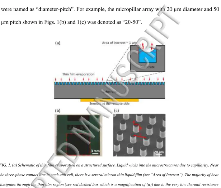
passive liquid transport5,6,8 (Fig. 1(a)). Furthermore, near the three-phase contact line, there is a
several micron thin liquid film (defined as the thin film region in this work; see red dashed box of
the zoomed in unit cell in Fig. 1(a))5–8. The heat transfer across this liquid thin film is of very low
thermal resistance, which has been shown to account for most of the heat dissipation during
evaporation12.
Measuring the temperature of this thin film region is, therefore, key to understanding the
fundamental enhancement mechanisms and optimization of the structure geometry. However,
directly probing local temperature of the thin film region is difficult using contact-based
3
placed on the backside of the sample (Fig. 1(a)) and thus can only characterize remotely the
thermal effects averaged over several millimeters rather than locally on the front structured
surface8. On the other hand, infrared thermometry, while capable of providing some temperature
information of the front side, has poor spatial resolutions (~10-30 µm)14,15 and is subject to large
temperature uncertainties (~5°C) when measuring the microscale thermofluidic system16. The
other weakness of infrared thermography is that it does not work well at temperatures below 50 or
70 °C (as there are not enough photons emitted in the 3-5 μm band at these low temperatures).
In this work, we developed a non-contact, in situ temperature measurement approach using
micro-Raman thermometry to investigate thin film evaporation from microstructured surfaces. Due to the superior spatial resolution (≈ 1 µm) and high temperature sensitivity (≈ 0.5 °C), micro-Raman thermometry has been widely used to measure the localized temperature rise11,12 for various
semiconductor materials17–19and microelectronic devices20,21. Meanwhile, the capability of
micro-Raman in studying phase change heat transfer has not yet been demonstrated. Here, we used silicon
micropillar arrays (Figs. 1(b) and 1(c)) as a platform for probing thin film evaporation with
micro-Raman. Since silicon emits strong Raman scattering, we can directly focus the laser excitation on
the top of each silicon micropillar and measure the temperature of the thin film region. By using
this technique for various micropillar arrays, we can obtain insights into both the local thin film
region and the temperature distribution of the entire structured surface. Additionally, the general
thermometry method is not restricted to understand thin film evaporation, but can be also widely
applied to study many thermofluidic problems at the microscale.
We fabricated test samples with a total microstructured area of 1 cm2 (red dashed box in Fig. 1(b)).
The cylindrical micropillars have diameters d of 20 µm and heights h of 50 µm (see the scanning
4
from 30 µm to 100 µm to investigate the geometrical effects on thin film evaporation. On the
backside of the sample, we deposited a 150 nm thick platinum layer which supplies uniform heat
flux to the structured area (see Supplementary S1 for details). In this work, all structured samples
were named as “diameter-pitch”. For example, the micropillar array with 20 µm diameter and 50 µm pitch shown in Figs. 1(b) and 1(c) was denoted as “20-50”.
FIG. 1. (a) Schematic of thin film evaporation on a structured surface. Liquid wicks into the microstructures due to capillarity. Near the three-phase contact line in each unit cell, there is a several micron thin liquid film (see “Area of Interest”). The majority of heat dissipates through the thin film region (see red dashed box which is a magnification of (a)) due to the very low thermal resistance across it. Temperature sensors such as RTDs are typically placed on the backside of the substrate which is far away from the thin film region. (b) Image of the front side of a representative fabricated silicon test sample. The red dashed box represents the 1 cm2
structured area where evaporation occurs. (c) SEM image of the micropillar array on the structured area, where d, h and l represent the pillar diameter, pillar height, and pitch of the array, respectively.
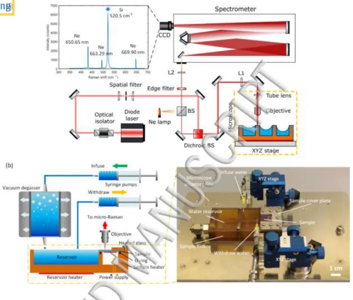
To obtain accurate local temperature measurements, we designed and built a custom micro-Raman
system. Micro-Raman spectroscopy analyzes the inelastic scattering between an incident photon
5
frequency (also known as the Raman shift or Raman peak position) is temperature dependent,
micro-Raman spectroscopy can be used to measure the temperature. Fig. 2(a) shows the schematic
of the optical path (see Supplementary Material S2 for details on the micro-Raman setup). The
Raman scattering was excited by a 633 nm wavelength diode laser. This laser excitation was
focused by a 50X microscope objective with a numerical aperture (NA) of 0.55. The corresponding
laser spot diameter on the micropillar was ~ 1.5 μm. The uncertainty of the measured Raman peak
position was controlled within 0.01 cm-1 and the corresponding temperature uncertainty was below
0.5 °C (see Supplementary Material S2 for the uncertainty analysis). We used a low laser power
at 0.5 mW to avoid laser heating effect (see Supplementary Materials S2 for the laser heating
analysis). We showed an example Raman peak of silicon (marked as star in Fig. 2(a)), calibrated
by neon emission lines (see the spectrum shown in Fig. 2(a)). We measured the temperature of the
sample by detecting the change of Raman peak position. The change of Raman peak position and
the corresponding temperature rise is given by,
Δ𝜔 = 𝐴(𝑇 − 𝑇𝑟𝑒𝑓) (1)
where Δ𝜔 is the change of Raman peak position, (𝑇 − 𝑇𝑟𝑒𝑓) is the temperature rise with respect to the reference temperature 𝑇𝑟𝑒𝑓. We used the ambient temperature as the reference temperature in this study. The proportionality constant 𝐴 is known as the linear temperature coefficient of the structured sample, which was -0.0225± 0.002 cm-1/°C (see Supplementary Materials S3 for
temperature coefficient measurement). The measured temperature coefficient in this work shows
good agreement with the results reported by Beechem et al.21 (-0.022 cm-1/°C).
We integrated the micro-Raman setup with a thin film evaporation test rig. Fig. 2(b) shows the
6
second syringe pump to control the reservoir water level to avoid flooding on the structured area
(see the magnified image of Fig. 2(b) for details of the sample fixture). The reservoir was
maintained at 40 °C (see Supplementary Material S4 for details of experimental procedures). We
characterized heat loss through the system by measuring a non-wetting structured surface (see
Supplementary Material S5 for details of heat loss characterization). In the absence of evaporation,
the heating power represents the heat loss Qloss which is proportional to the temperature rise
(proportionality is 0.060 W/°C). Therefore, the heat flux q” through evaporation of water was
given by,
𝑞′′ =𝑄𝑡𝑜𝑡− 𝑄𝑙𝑜𝑠𝑠
𝑆 (2)
7
FIG. 2. (a) Optical path of the custom micro-Raman setup interfaced with thin film evaporation setup developed in this work. “BS” and “L” represent the beam splitter and lens, respectively. Dotted black box shows an example Raman spectrum of silicon (indicated by the star) with 633 nm excitation. The other three peaks are the neon emission lines used for calibration. (b) Schematic of the thin film evaporation test rig integrated with a flow loop which is interfaced with the micro-Raman system. Right: Optical image of the sample fixture. The sample fixture was placed on a microscope adaptor plate. Two XYZ stages were used to hold the bended needles, which infuse/withdraw water. The structured sample was fixed by sample cover plate on the right side.
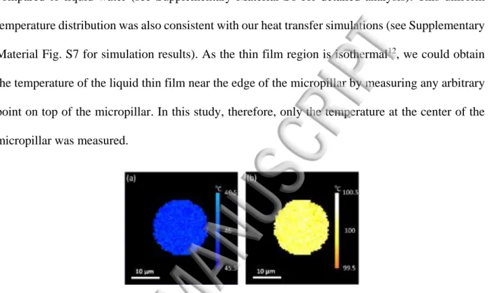
We experimentally demonstrated the high spatial resolution and temperature sensitivity of
micro-Raman thermometry by measuring the temperature distribution on top of a single micropillar. As
shown in Fig. 3, we performed temperature mapping (0.5 μm scanning step size) using
8
applied heat flux q” of 1 W/cm2 and 21 W/cm2. In both cases, as expected, the temperature was
very uniform at 46 °C and 100 °C due to the relatively high thermal conductivity of silicon
compared to liquid water (see Supplementary Material S6 for detailed analysis). This uniform
temperature distribution was also consistent with our heat transfer simulations (see Supplementary
Material Fig. S7 for simulation results). As the thin film region is isothermal12, we could obtain
the temperature of the liquid thin film near the edge of the micropillar by measuring any arbitrary
point on top of the micropillar. In this study, therefore, only the temperature at the center of the
micropillar was measured.
FIG. 3. Top-down view of the temperature distribution of a single micropillar located at the center of a 20-60 sample with an applied heat flux of (a) q” = 1 W/cm2 and (b) q” = 21 W/cm2. The step size of the micro-Raman temperature mapping was 0.5 µm.
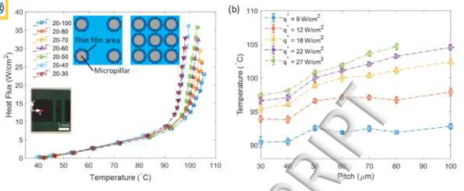
To understand the effects of micropillar array geometries on heat transfer performance, we
characterized the evaporation process by measuring the local temperature of the liquid thin film at
various heat fluxes and on different structured samples. The micro-Raman probe was focused on
a micropillar located at the center of the structured area (see the inset of Fig. 4(a)) for all samples.
The heat flux q” was increased gradually from 0 to 30-40 W/cm2 until dryout was observed. We
determined the dryout when the liquid at the end of the structured area started receding. The dryout
heat fluxes were relatively low because of the long wicking length L (1 cm) chosen in this study,
and qdryout scales with 1/L2. Fig. 4(a) shows the evaporation curves of different structured samples.
9
film region was well below the saturation point (100 oC at 1 atm), the evaporation was limited by
vapor diffusion in the air and increased slowly with temperature rise. The heat dissipation in this
regime significantly relied on the sensible cooling of the liquid as well as the liquid-to-vapor phase
change. When the temperature approached the saturation point, evaporation became the dominant
heat transfer mechanism and the heat flux increased sharply with a slight temperature rise. On the
20-100 sample, the maximum temperature was found to be 106 °C, indicating the liquid thin film
was in a superheated state during evaporation. This maximum temperature decreased as the pitch
decreased. The evaporation curves generally shifted to the left with decreasing pitch, indicating
that higher heat transfer coefficients were achieved on the smaller pitch samples. Fig. 4(b) shows
the liquid film temperature as a function of the micropillar pitch at various heat flux conditions.
The effect of small pitch in reducing the liquid film temperature was more significant at relatively
high heat fluxes (20-30 W/cm2) than at low heat flux conditions (below 15 W/cm2). For example,
when the heat flux was 27 W/cm2, the liquid film temperature was reduced by approximately 8 oC
when the pitch decreased from 80 μm to 30 μm. This improvement in evaporation heat transfer
can be explained by the increase in thin film area. With the decrease of the pitch, more thin film
regions around the micropillar were created per unit area, which offer more effective areas to
10
FIG. 4. (a) Evaporative heat flux as a function of temperature rise for various structured samples. The experiments were stopped when dryout was observed at the end of the structures. Inset: Optical image of sample showing the location of the measured temperature, i.e. the red spot. Schematic showing structure effects on thin film evaporation. Reduced liquid film temperature at small pitch sample is attributed to the creation of more thin film area. (b) The liquid film temperature as a function of micropillar pitch at a variety of heat fluxes. At the same heat flux, liquid film superheat was reduced as the pitch decreased. For the 100 μm pitch, dryout already occurred at 27 W/cm2 and therefore no data point is shown.
We also studied the effects of micropillar array geometries on the temperature distribution of a
structured surface sample. We scanned the temperature distribution from 1 mm to 9 mm along the
capillary flow direction on 20-30, 20-80, and 20-100 samples (see the XY coordinate in the inset
of Fig. 5). The heat flux q” was maintained at approximately 22 W/cm2. As this heat flux was
significantly smaller than the dryout heat flux for the 20-30 sample (33 W/cm2), the meniscus in
each unit cell was almost flat, resulting in similar local heat transfer coefficients (see the schematic
of the inset of Fig. 5). Therefore, the temperature distribution on the 20-30 sample was uniform
along the flow direction. However, nonuniform temperature distributions were observed on the
20-80 and 20-100 samples (Fig. 5). Generally, along the flow direction, the temperature of the
micropillar increased first and then dropped slightly (as small as 1-2 °C). The increase of
temperature at the inlet of the structured surface is attributed to the decrease in sensible cooling
11
Supplementary Material S4 for more details). The slight decrease of temperature from the middle
part (3 mm for 20-100 and 4 mm for 20-80 samples) to the end (9 mm) is due to the interface shape
change. As this heat flux (q” = 22 W/cm2) was close to the dryout heat fluxes of 20-80 and 20-100
samples (26 W/cm2 and 23 W/cm2, respectively), the apparent contact angle of the liquid in the
last unit cell approached the receding contact angle (see the schematic of the inset of Fig. 5).
Consequently, the liquid films near the three-phase contact line became thinner along the flow
direction. Since the thinner liquid film had smaller thermal resistance, the temperature decreased
from the middle of the sample towards the end gradually.
FIG. 5. Temperature distribution along the flow direction of different structured samples at a constant heat flux q” = 22 W/cm2.
When the heat flux approached the dryout heat flux of the sample, the temperature increased first due to the sensible cooling and heat transfer to the reservoir and then decreased 1-2 °C gradually from the middle part to the end due to the change of the
meniscus liquid-vapor interface. Inset: Optical image on the front side of the test sample and the XY coordinate used for scanning. Schematics of the meniscus liquid interface varying along the capillary flow direction on different structured samples.
In summary, we showed the use of micro-Raman spectroscopy for in situ temperature
measurement of liquid thin film in micropillar arrays during evaporation, where 1.5 µm spatial
resolution and 0.5 °C temperature sensitivity were achieved. We precisely measured the liquid
12
We characterized evaporation from micropillar arrays of different geometries, showing that the
liquid film temperature reduced as the pitch of the micropillar decreased due to the increase of thin
film area. We also found the nonuniform temperature distribution occurred along the flow direction
when the sample approached dryout. The high resolution local temperature measurement method
presented in this work is not only beneficial to the characterization and optimization of thin film
evaporation but can be potentially utilized to reveal physical insights into a variety of other phase
change heat transfer processes such as condensation and pool/flow boiling on structured surfaces.
See supplementary materials for more information on sample fabrication, experimental setup,
sample calibration, additional experimental results, simulation and data analysis.
L. Zhang and Y. Zhu contributed equally to this work.
The authors would like to acknowledge Arny Leroy and Dion S. Antao for valuable discussions,
and the MIT Microsystems Technology Lab for fabrication staff support, discussion and use of
equipment. L. Zhang gratefully acknowledges funding support from the MIT/MTL GaN Energy
Initiative and the Singapore-MIT Alliance for Research and Technology (SMART) LEES
Program. Y. Zhu acknowledges funding support provided by the Office of Naval Research (ONR)
with Dr. Mark Spector as program manager under Award No. N00014-15-1-2483. Z. Lu
acknowledges funding support from the Air Force Office of Scientific Research with Dr. Ali Sayir
as the program manager under Award No. FA9550-15-1-0310. The authors also acknowledge the
DURIP program through ONR for the support of the equipment.
1 T.W. Kenny, K.E. Goodson, J.G. Santiago, E. Wang, J. Koo, L. Jiang, E. Pop, S. Sinha, L.
13
2 F. Zhao, X. Zhou, Y. Shi, X. Qian, M. Alexander, X. Zhao, S. Mendez, R. Yang, L. Qu, and G.
Yu, Nat. Nanotechnol. 13, 489 (2018).
3 A.E. Kabeel and E.M.S. El-Said, Desalination 341, 50 (2014).
4 G. Ni, G. Li, S. V. Boriskina, H. Li, W. Yang, T. Zhang, and G. Chen, Nat. Energy 1, 16126
(2016).
5 H.J. Cho, D.J. Preston, Y. Zhu, and E.N. Wang, Nat. Rev. Mater. 2, 1 (2016).
6 Y. Zhu, D.S. Antao, Z. Lu, S. Somasundaram, T. Zhang, and E.N. Wang, Langmuir 32, 1920
(2016).
7 Z. Lu, K.L. Wilke, D.J. Preston, I. Kinefuchi, E. Chang-Davidson, and E.N. Wang, Nano Lett.
17, 6217 (2017).
8 S. Adera, D. Antao, R. Raj, and E.N. Wang, Int. J. Heat Mass Transf. 101, 280 (2016).
9 D.F. Hanks, Z. Lu, J. Sircar, T.R. Salamon, D.S. Antao, K.R. Bagnall, B. Barabadi, and E.N.
Wang, Microsystems Nanoeng. 4, 1 (2018).
10 M.G. Ancona, S.C. Binari, and D.J. Meyer, J. Appl. Phys. 111, 074504 (2012).
11 K.R. Bagnall, E.A. Moore, S.C. Badescu, L. Zhang, and E.N. Wang, Rev. Sci. Instrum. 88,
113111 (2017).
12 R. Ranjan, J.Y. Murthy, and S. V. Garimella, Int. J. Heat Mass Transf. 54, 169 (2011).
13 H.K. Dhavaleswarapu, S. V. Garimella, and J.Y. Murthy, J. Heat Transfer 131, 061501 (2009).
14 C.D.S. Brites, P.P. Lima, N.J.O. Silva, A. Millán, V.S. Amaral, F. Palacio, and L.D. Carlos,
14
15 M.M. Kim, A. Giry, M. Mastiani, G.O. Rodrigues, A. Reis, and P. Mandin, Microelectron.
Eng. 148, 129 (2015).
16 T.-L. Liu and C. Pan, Appl. Therm. Eng. 94, 568 (2016).
17 I. Calizo, A.A. Balandin, W. Bao, F. Miao, and C.N. Lau, Nano Lett. 7, 2645 (2007).
18 N.A. Lanzillo, A. Glen Birdwell, M. Amani, F.J. Crowne, P.B. Shah, S. Najmaei, Z. Liu, P.M.
Ajayan, J. Lou, M. Dubey, S.K. Nayak, and T.P. O’Regan, Appl. Phys. Lett. 103, 093102 (2013).
19 R. Yan, J.R. Simpson, S. Bertolazzi, J. Brivio, M. Watson, X. Wu, A. Kis, T. Luo, A.R. Hight
Walker, and H.G. Xing, ACS Nano 8, 986 (2014).
20 M. Kuball, G.J. Riedel, J.W. Pomeroy, A. Sarua, M.J. Uren, T. Martin, K.P. Hilton, J.O.
Maclean, and D.J. Wallis, IEEE Electron Device Lett. 28, 86 (2007).
21 T. Beechem, S. Graham, S.P. Kearney, L.M. Phinney, and J.R. Serrano, Rev. Sci. Instrum. 78,
View publication stats View publication stats