HAL Id: hal-01225364
https://hal.archives-ouvertes.fr/hal-01225364
Submitted on 6 Nov 2015
HAL is a multi-disciplinary open access
archive for the deposit and dissemination of
sci-entific research documents, whether they are
pub-lished or not. The documents may come from
teaching and research institutions in France or
abroad, or from public or private research centers.
L’archive ouverte pluridisciplinaire HAL, est
destinée au dépôt et à la diffusion de documents
scientifiques de niveau recherche, publiés ou non,
émanant des établissements d’enseignement et de
recherche français ou étrangers, des laboratoires
publics ou privés.
EMC performance analysis of a Processor/Memory
System using PCB and Package-On-Package
Etienne Sicard, Alexandre Boyer, Priscillia Fernandez-Lopez, An Zhou,
Nicolas Marier, Frédéric Lafon
To cite this version:
Etienne Sicard, Alexandre Boyer, Priscillia Fernandez-Lopez, An Zhou, Nicolas Marier, et al.. EMC
performance analysis of a Processor/Memory System using PCB and Package-On-Package. 10th
International Workshop on the Electromagnetic Compatibility of Integrated Circuits (EMC Compo
2015), Nov 2015, Edimburgh, United Kingdom. 6p. �hal-01225364�
EMC performance analysis of a Processor/Memory
System using PCB and Package-On-Package
Etienne Sicard
(1), Alexandre Boyer
(1), Priscila Fernandez-Lopez
(2), An Zhou
(3), Nicolas Marier
(2), Frédéric Lafon
(2)(1) INSA, University of Toulouse, 135 av. de Rangueil, 31077 Toulouse, France (2) VALEO – GEEDS, 2 Rue André Boulle, 94046 Créteil, France
(3)
VALEO, 34 rue Saint André, 93000 Bobigny, France
Contacts: (1) [email protected], (2) [email protected]
Abstract—In this paper, the signal integrity (SI) and
Electromagnetic Compatibility (EMC) performance of System-On-Chip (SoC) and stacked memory using Package-On-Package (PoP) technology is investigated. The reconfiguration of the IC-EMC software platform to PoP is described. From an existing 2D assembly using a discrete 65-nm SoC product, the benefits of PoP integration using a next-generation 28-nm product with stacked memory are analyzed, based on simulation and predictive analysis performed using IC-EMC software platform.
Keywords- Signal integrity; EMC; Microcontroller and memory; PoP; Equivalent bus model; Near-Field Scan; IBIS
I. INTRODUCTION
Integrated circuits are manufactured with increased miniaturization of components enabling increasingly higher performance, reduced power consumption and costs. The speed of data exchanges between IC mounted in conventional packages is severely limited, due to long interlinks through conductive layers of a circuit board, and its associated inductive, resistive and capacitive effects. Package-on-Package (PoP) is considered as an efficient low cost and adaptable approach to high-performance packaging. Often considered as an intermediate step between conventional 2D assembly and 3D stacking of dies, PoP do not require costly Through-Silicon-Vias (TSV) and interposer technology, while demonstrating significant benefits in terms of density, signal integrity, reduced propagation delays, increased operating frequencies and enhanced power efficiency. Packages are stacked on the top of each other, with low-cost Trough-Molded Vias (TMV) for interconnection between Ball-Gate-Arrays (BGA).
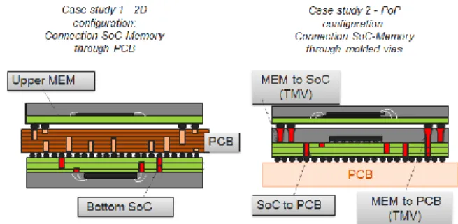
In this paper, the signal integrity and EMC performances of a PoP assembly of SoC and SRAM memory are analyzed. We consider two versions of a SoC/SRAM structure (Fig. 1): one is a high-density-interconnect (HDI) miniature printed-circuit-board with a µ-BGA SoC (65-nm) on one side [1], the SRAM memory on the other side [2], with the shortest possible interconnects through the HDI board. This case study is analyzed in section II. The second case study is a stacking of a NG µ-BGA SoC [3] and a mobile DDR memory [4] based on PoP technology. This configuration is analyzed in section 3. Strictly speaking, the 2 systems are not identical as the ICs, packages and vias are fabricated in different technologies.
Figure 1. Cross-section of the two case studies : connection through PCB (top), connection through Package-on-package (bottom)
II. ANALYSIS OF THE 2DCASE STUDY
We detail in this section the case study including a SoC and memory mounted on a high-density-interconnect (HDI) miniature printed-circuit-board (PCB). The µ-BGA package of the SoC is placed on one side of the PCB [1], the SRAM memory on the other side [2], with the shortest possible interconnects through the HDI board,
A. Technology analysis
An in-depth technology analysis of the SoC and the memory involved in case study 1 has been performed inhouse, producing metrics of the internal structure of the IC and PCB (Fig. 2). Although the ball pitch, size, package thickness of both packages are just a confirmation of the data sheet information [1][2], the die size, type of package leads, bonding length, HDI layer configuration are extracted from these analyses.
Figure 2. Technology analysis of the SoC involved in case study 1, revealing the IC die size, type of die/lead connection and HDI PCB
Figure 3. Technology analysis of the 512Mb mobile DDR involved in case study 1 [2]
These parameters have direct consequences on EMC performance of the chip as bondings may radiate [4] and the IC die size itself may couple to structures like the septum of the TEM cell.
B. IBIS analysis of the SoC and DDR ICs
An IBIS file is provided by the SoC design company Texas Instruments, which mention the PakSi-E tool from Apache ™, enabling full package R,L,C extraction.
TABLE I. ANALYSIS OF IBISISSUES AND IMPACT ON EMC
Facts Impact on EMC Importance Corrections
Missing power pins PDN cannot be reconstructed, power domains unknown
High Add pins manually using data sheet Assign power domain names Missing SATA and clocks Signal integrity on SATA not available. Clock models unknown
High for clock domain immunity and SSN on SATA
Add first order models based on data sheet information or similar IC ports I/V curves non monotono us
Ion values may not be reliable. Should be cross-checked with data sheet
High for SSN analysis and IO port immunity estimation
Modify I/V tables or take data sheet values as references Missing
[Pin
Mapping]
Link between IOs and supply domains unknown
Medium Find information on datasheet and create section No [EMI] Clues for parasitic
emission
Medium Possible first order model No [Composit e current] On-chip decoupling and PDN parameters
High Possible first order model
As listed in Table 1, several issues are raised due to the missing power supply pins, missing SATA, clocks models, non-monotonous I/V tables, etc. We apply some corrective actions as listed in Table 1: declaration of all power supply pins, description of missing IO pins with models close to data-sheet information etc. We also add hidden keywords for 3D reconstruction in IC-EMC [3], with a result shown in Fig. 5. From the power and ground floorplan (Fig. 6), we may observe that the power pin count is unbalanced and large IO regions suffer a lack of sufficient dedicated supply. The IBIS file of the DDR is available from the ISSI company web site [2]. The IBIS quality is good, all supply pins are declared, and I/V curves are consistent with the data-sheet specification.
Figure 4. Loading the IBIS file with IC-EMC reveals missing pins and some violations of IBIS basic rules
Figure 5. Improved IBIS model of the SoC including hidden keywords for 3D reconstruction using the IC-EMC freeware tool [3]
Figure 6. Floorplan analysis of the supply rails: unbalanced VDD/VSS and large areas without dedicated IO supply
Figure 7. The IBIS model quality of the DDR memory is globally satisfactory, except minor issues.
The only issues concern a lack of information for clamps and non-monotonous I/V in –VDD..0V region (Fig. 7). The floorplan of the DDR memory reveals a balanced power situation, and a regrouping of DDR IOS north to the IC, which may indicated a dominant orientation of the port parasitic emission.
C. Signal Integrity on DDR bus
It can also be seen from Figs. 2 and 3 that the PCB is made of 12 layers with varying oxide thickness. The layer dimensions are evaluated from cross-section views provided by the technology analysis and cross-checked with PCB provider’s information. We benefit of measured waveforms performed using an oscilloscope with active probe (Fig. 8).
Figure 8. Measurement of signal waveforms on the DDR bus, exhibiting rise and fall time within the range 600-700ps.
D. Modelling
Our first goal is to match SI measurements using a simple model of the DDR link. Our second goal is to match near-field scan and TEM cell measurements. From the track dimensions and BGA package characteristics, we derive the typical impedance Z0 and associated R,L,C values for each portion of the DDR path, including the power distribution network (PDN) of the DDR to account for non-ideal supply voltage (Fig. 9). A detailed description of the schematic diagrams used for this simulation may be found in [5]. Fig. 10 shows the simulated DDR link with good agreement with measurements of Fig. 8, by taking into account the measurement probe (around 5pF) which distorts signals significantly.
Figure 9. Modeling of the DDR path including non-ideal PDN.
Figure 10. Simulation of the DDR path using IC-EMC. Full details may be found in [5].
E. Emission measurements
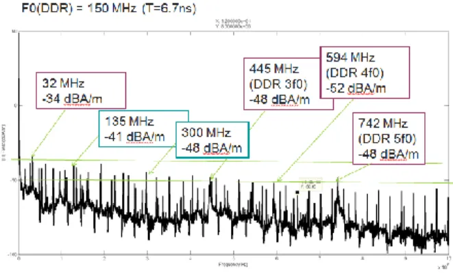
Both sides of the package have been scanned using a near-magnetic field scanner with a probe loop of 1mm diameter. The cumulated field (Fig. 11) shows a dominant radiation above the SoC package, and a clear hot spot close to the DDR region. From the spectrum extracted at the location of peak magnetic field (Fig. 12), we observe complex harmonics with two interleaved contents: one based on 32 MHz (core), the other based on 50 MHz harmonics (DDR). The dominant radiating elements are the bondings of the SoC (double structure with large bonding length far from ground), and in a second order effect, the memory bonding which is however much shorter.
Figure 11. Cumulated magnetic field from Near-field scan measurements showing a hot spot above the SoC package
Figure 12. Spectrum at the location above the SoC with maximum magnetic field, showing a very wide and complex set of harmonics
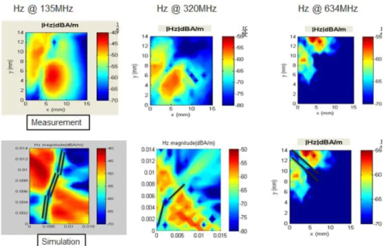
Figure 13. Measured and simulated near-field scan of the SoC at 3 different frequencies, at an altitude of 3mm above the ground plane
Therefore, we use equivalent radiating inductance to match measured and simulated magnetic field from the SoC, as illustrated in Fig. 13.
III. POP CASE STUDY
In this section, a New Generation (NG) SoC [3] mounted on a micro-BGA and a SRAM memory [4] stacked using Package-On-Package technology is described. The proposed analysis is only prospective as no PoP prototype was available at the time of this study, except the preliminary specifications and IBIS preliminary informations.
A. Handling Pop in IC-EMC
The tool IC-EMC has been modified in order to handle multiple BGA package stacking as shown in Fig. 14. A new keyword “[Pop]” was added in IBIS as a separator for different pins. Hidden keywords may also be assigned separately to a maximum of 8 different ICs, enabling to handle different ball pitch and die size for each stacked layer. In 2D, each IC may be addressed separately.
Figure 14. Handling PoP description in IC-EMC with up to 8 package/dies and different ball pitch
Figure 15. Analysis of power domains of the NG-SoC
The floorplan of the NG-SoC (Fig. 15) reveals a regular and symmetrical spread of power domains. The DDR IOs shared with the memory are clearly oriented north (Fig. 15 – right). The floorplan of the memory (Fig. 15) reveals non-symmetrical VDD/VSS assignments (Fig. 16). VDD pins are missing in the lower part of the die, leading to an unbalanced current flow and potential radiating loops.
Figure 16. Analysis of power domains of the SDRAM memory
B. Signal Integrity Performance Predictions
The prospective signal integrity analysis is based on a similar approach as described in section II. The major change is the suppression of the 12-layer PCB, replaced by the BGA stack. The new feature in the PoP is the through-mold-via (TMV) which serves as vertical interconnect between BGA packages. The TMV is mostly inductive but its crosstalk capacitance Cx to adjacent TMVs is significant due to the vertical dimensions of the via (340µm) and the short distance between vias in the TMV array. Details on R,L,C values used in the prospective signal integrity analysis are given in table II.
The predictive signal integrity analysis on one single DQ data line connecting the NG-SoC and the stacked mDDR is reported in Fig. 18. The inductive nature of the tracks combined with the high data rate (one symbol every 2.5ns) generates overshoots and undershoots with important harmonic contents at 800 and 1200 MHz. Corrective actions such as impedance adaptation, serial resistive load or current reduction may be taken to reduce these effects.
Figure 17. Overview the signal integrity simulation in the case of PoP prototype
TABLE II. DETAILS ON THE POPMODELLING
N ° Item Description R () L (H) C (F) 1 NG-SoC buffer 25 mA Pull-up/down with C_comp capa, 400 MHz 1.24 p 2 Microbal l 20 x 20 µm Micro-bump to DSP package 300 m (@ 1GHz) 20 p 50 f (Cx) 3 BGA track 5 mm track 20µm width, 20µm spacing, 17µm thick over GND 0.63 (@ 1GHz) 2.24 n 361 f 4 TMV 340 x 300µm 30 m (@ 1GHz) 0.3 n 1.2 p (Cx) 5 Mem track 5 mm track 20µm width, 20µm spacing, 17µm thick over GND (radiating) 0.63 (@ 1GHz) 2.24 n 361 f 6 Bonding 3 mm bonding 25µm diameter (radiating) 2 n 7 Mem input
Input pad, mostly C_comp
10 K pull down
4pF
This type of simulation also demonstrates the role of predictive simulation: a wide set of IO configuration, drive strength and termination options is usually proposed, and such early-phase analysis may give some guidelines for keeping the overall DDR bus EMI compliant.
We combine 32 DQ data lines and consider realistic mDDR chronograms as reported in Fig. 19, extracted from the JEDEC standard for DDR2. We assume a Read Latency (RL) of 3 and a Write Latency (WL) of 1. The maximum switching activity of the DQ port is around 25% of a full continuous activity. The duty cycle induces sub-harmonics in relation with 4-cycle (100 MHz) and 8-cycle delays (50MHz).
Figure 18. Predictive signal integrity simulation in the case of PoP prototype
Figure 19. Typical chronograms of a DDR link with READ and WRITE cycles, RL=3, WL=1 [Jedec]
We follow the same model-order reduction technique as used in a previous work [6] to extrapolate the 32-bit bus conducted and radiated emission, while keeping the schematic diagram simple and straightforward. We consider here three geographical domains, meaning 3 radiating dipoles. In step 1 (Fig. 21), all buffers are considered to switch synchronously (0x0000, 0xFFFF), which is equivalent to multiplying the single DQ0 activity (Fig. 18) by 32. We apply a 25% duty cycle to match the mDDR2 specification recalled in Fig. 19. We only consider 10% of the current due to the fact that DQ data is random. We then apply a screening factor depending on the shielding efficiency of the upper package. Long bondings far from any ground reference act as good antennas, while short bondings with local ground only radiate a fraction of the switching noise (Fig. 21). We consider the ground reference 1mm below the radiating dipoles Fig. 21 left (worst case). The radiation pattern would be significantly reduced by considering the ground reference 100-200 µm below the bondings (Fig 21. Right) thanks to an embedded ground plane in the memory BGA.
Figure 20. Predicting NF emission of the DDR bus
Figure 21. The upper structure of the die, bonding and ground reference plays a key role in the PoP radiated emission
Figure 22. Splitting the bonding inductance into radiating and non-radiating parts to account for non-radiating efficiency of the BGA
Figure 23. Predictive PoP radiated magnetic field 5mm above the ground plane using IC-EMC [5]
The 32-bit bus is split into 3 domains (Fig. 20) to account for the unbalanced pin assignment of DQ data. Each domain represents approximatively 10 DQ wires in parallel. The driver strength is 10 times the DQn driver, by acting on the equivalent width of the pull-up and pull-down devices. The schematic diagram considers two inductances instead of one for the radiating structure: one part is described in the X,Y,Z space and radiate, the other part is not described in space and do not radiate. This approach enable to modulate the radiating current according to the fact that DQ data is random and the BGA structure acts as a moderate shielding. The 10% radiation applied in the inductance value (20pH for radiating part, 200pH for non-radiating part in Fig. 22) come from experience acquired in NFS and model tuning of similar BGAs. Using the NF simulator of IC-EMC, we obtain the result of Fig. 23, with a peak magnetic field around -65dBA/m, that is a significant reduction as compared to 2D configuration. However, this forecast should be matched with real-case measurements, which are unfortunately not available at the time of this publication. For an improved prediction of the radiated emission, more attention should be paid to the vertical structures in the PoP which may radiate such as TMV’s situated on the border of the 3D structure. Also, the power-supply noise and non-perfect IO supply should also be considered. Further bus activities such as the command bus (CA in Fig. 19) could also be added.
IV. CONCLUSION
In this paper, we conducted signal integrity simulations of the DDR bus connecting a SoC and a memory placed on both sides of miniature PCB. We highlighted some issues in the IBIS quality of the 2 devices under test. We could also match measurements and simulations of magnetic field based on radiating elements. From these results, we could extrapolate the potential near-magnetic field emitted by a Package-on-package structure with a BGA memory on-top. Future work will concern of these simulations and associated approximations with real-case measurements.
REFERENCES
[1] OMAP-L138 C6-Integra™ DSP+ARM® Processor Data sheet, on-line at www.ti.com, Oct. 2011
[2] IS43LR16320B, IS46LR16320B 8M x 16Bits x 4Banks Mobile DDR SDRAM data sheet, on-line at www.issi.com , april 2012 [3] DM3730, DM3725 Digital Media Processors Data Sheet, PDF on
line at www.ti.com, July 2011
[4] Mobile LPDDR2 SDRAM MT42L32M16D1 data sheet, on-line at www.micron.com,
[5] E. Sicard, A. Boyer IC-EMC v2.5 User's Manual, Oct. 2011, 260 pp, ISBN 978-2-87649-061-1, www.ic-emc.org
[6] E. Sicard, Wu Jian-fei, Li Jian-cheng, “Signal integrity and EMC performance enhancement using 3D Integrated Circuits – A Case Study”, EMC Compo 2013, Nara, Japan
[7] A. Boyer, E. Sicard, “Signal integrity simulation of a SoC-DDR Memory mounted on a HDI PCB”, Application note, www.ic-emc.org, 2015
[8] JEDEC STANDARD, Low Power Double Data Rate 2 (LPDDR2), Ref. JESD209-2B, 2010, www.jedec.org
![Figure 5. Improved IBIS model of the SoC including hidden keywords for 3D reconstruction using the IC-EMC freeware tool [3]](https://thumb-eu.123doks.com/thumbv2/123doknet/14263437.489545/3.893.47.430.468.814/figure-improved-ibis-including-hidden-keywords-reconstruction-freeware.webp)

![Figure 23. Predictive PoP radiated magnetic field 5mm above the ground plane using IC-EMC [5]](https://thumb-eu.123doks.com/thumbv2/123doknet/14263437.489545/7.893.94.391.776.999/figure-predictive-radiated-magnetic-field-ground-plane-using.webp)
