HAL Id: tel-00666073
https://tel.archives-ouvertes.fr/tel-00666073
Submitted on 3 Feb 2012
HAL is a multi-disciplinary open access archive for the deposit and dissemination of sci-entific research documents, whether they are pub-lished or not. The documents may come from teaching and research institutions in France or abroad, or from public or private research centers.
L’archive ouverte pluridisciplinaire HAL, est destinée au dépôt et à la diffusion de documents scientifiques de niveau recherche, publiés ou non, émanant des établissements d’enseignement et de recherche français ou étrangers, des laboratoires publics ou privés.
Achille Francone
To cite this version:
Achille Francone. Materials and anti-adhesive issues in UV-NIL. Materials. Institut National Poly-technique de Grenoble - INPG, 2010. English. �tel-00666073�
Délivrée par l’Institut Polytechnique de Grenoble
N° attribué par la bibliothèque |__|__|__|__|__|__|__|__|__|__|
T H E S E pour obtenir le grade de
DOCTEUR DE L’UNIVERSITE DE GRENOBLE
Spécialité : « 2MGE Matériaux, Mécanique, Génie civil, Electrochimie » préparée au Laboratoire des Technologies de la Microélectronique (LTM-CNRS) dans le cadre de l’Ecole Doctorale « I-MEP2 Ingénierie Matériaux Mécanique Energétique
Environnement Procéés Production »
présentée et soutenue publiquement par
Achille FRANCONE
Le 9 Décembre 2010
Materials and anti-adhesive issues in UV-NIL
Directeur de thèse: BOUSSEY Jumana
JURY
Although a lot of efforts were necessary to write this PhD thesis, I feel really satisfied about the final result. A lot of persons contributed directly and indirectly, more or less, to the achievement of this work.
I am grateful to all the persons that accepted to participate to the jury of my thesis: Pr. AUZELY-VELTY Rachel, Dr. KEHAGIAS Nikolaos, Dr. IOJOIU, Cristina, Dr. ZELSMANN Marc, Dr. BOUSSEY Jumana, Dr. SOPPERA and Pr. SCHLATTER Guy, with the last two that accepted to evaluate my manuscript as rapporteurs.
I really appreciated the hospitality shown during this three-year thesis work at the Laboratoire des Technologies de la Microélectronique (LTM) in Grenoble (France) inside the CEA-LETI-Minatec center. I would like indeed to thank Dr. JOUBERT Olivier t, LTM Head, for enabling me to carry out this work in an excellent technical and scientific environment.
I am grateful to Région Rhône-Alpes for financing my three years PhD fellowship.
Special thanks go to Dr. BOUSSEY Jumana my thesis director for having made this work possible. She launched me on this adventure, and I have received high-value support from her throughout the thesis. Her patience in front of difficult situations taught me a lot.
Sincere thanks go to Dr. ZELSMANN Marc, my daily supervisor at LTM lab, with whom I have spent uncountable hours engaged in enjoyable and enriching discussions. His broad background in physics and engineering, his sportive spirit, his rigorous work and his methodology have contributed significantly to my scientific and human apprenticeship.
Then, I would like to thank a group of persons for the nice collaborations we had during my PhD, managing to get interesting results during different kinds of experiments. These persons are: Dr. POULAIN Christophe during nanoindentation experiments at CEA Grenoble-LETI-DIHS-Laboratoire de Caractérisation et de Fiabilité des Microsystèmes; LOMBARD Christophe and Dr. PEPIN-DONAT Brigitte during electron spin resonance experiments at CEA Grenoble-INAC- Laboratoire de Structure et Propriétés d’Architecture Moléculaires; Dr. IOJOIU, Cristina during Fourier Transform Infrared Spectroscopy experiments at CNRS-GrenobleLaboratoire d’Electrochimie et de Physicochimie des Matériaux et des Interfaces.
During my Phd I had also the possibility to collaborate and to run experiments away from Grenoble. In particular I had the pleasure to collaborate with Dr. ZOMPATORI Alberto, dependent of SOLVAY Solexis S.p.A., who hosted me in the Italian research and development centre at Bollate to select an anti-adhesive commercial product. His collaboration continued during all the experiments run on the product, giving precious advices over the interpretation of the results.
Many thanks go to HAATAINEN Tomi, that although several difficulties allows to me to run a week demolding force experiments in the Finnish VTT technical research centreat Espoo. Particular acknowledgments go to Pr. SOTOMAYOR TORRES Clivia who allowed to me to
France during my PhD.
A million thanks to my beloved family members back home in Italy, that encouraged me throughout the PhD time, sharing positive and negative moments.
Last but not least, my sincere thanks go to my lovely girlfriend Chiara, which gave me the moral support and motivations to go on, especially during the most critical moments of the PhD thesis writing period.
The works of research obtained after my three year Phd were well valorized. In fact, the results were presented during different events (international conferences, scientific day, summer school) and in different manners (journal publications, poster and oral presentations). These are listed below.
Journal Publications
1) D. Boutry, R. Galand, A. Beaurain, A. Francone, B. Pelissier, M. Zelsmann, and J. Boussey, “Mold cleaning and fluorinated anti-sticking treatments in nanoimprint lithography”, Microelectron Eng, 86 (4-6), p. 669-672, 2009.
2) M. Zelsmann, C. Alleaume, D. Boutry, A. Francone, A. Beaurain, B. Pelissier and J. Boussey, “Degradation and surfactant-aided regeneration of fluorinated anti-sticking mold treatments in UV nanoimprint lithography”, Microelectron Eng, 87 (5-8), p. 1029-1032, 2010.
3) M. Zelsmann, D. Boutry, A. Francone, C. Allaume, I. Kurt, A. Beaurain, B. Pelissier, B. Pépin-Donat, C. Lombard and J. Boussey , “Double-anchoring fluorinated molecules for anti-adhesion mold treatment in UV nanoimprint lithography”, J. Vac. Sci. Technol. B, 27(6), p. 2873-2876, 2009.
4) A. Francone, C. Iojoiu, C. Poulain, C. Lombard, B. Pépin-Donat, J. Boussey and M. Zelsmann, “Impact of the resist properties on the antisticking layer degradation in UV nanoimprint lithography”, J. Vac. Sci. Technol. B, 28(6), p. C6M72-C6M76, 2010.
5) N. Kehagias, A. Francone, M. Chouiki, M. Zelsmann, V. Reboud, R. Schoeftner and C. Sotomayor Torres, “Low temperature direct imprint of polyhedral silsequioxane (PSSQ) resist”, to appear in Microelectron Eng.
Poster Presentations
All the works of research above listed as journal publications were presented as well during international conferences. Those published in Microelectronic Engineering were exposed as poster presentations during the same year edition of Micro and Nano engineering conference; those published in Journal of Vacuum Science & Technology B were exposed as poster presentations during the same year edition of Electron, Ion, Photon Beam Technology and Nanofabrication conference. Another poster was presented, as follows:
N. Kehagias, R. A. Farrell, M. Zelsmann, A. Francone, M. Chouiki, V. Reboud, J. D. Holmes, M. A. Morris and C. Sotomayor Torres, “PSSQ templates fabricated by RUVNIL technique for graphoepitaxy”, Nanoprint and Nanoimprint Technology conference,
1) A. Francone, “Materials and process development of UV-based nanoimprint lithography”, NanoSciences Summer school, Tremblay (France), Jun 23-28, 2008.
2) A. Francone, “Développement de la lithographie par nano-impression assistée par UV (UV-NIL)”, Cluster Microéléctronique, Nanosciences et Nanoélectronique Scientific day, Grenoble (France), Oct 10, 2009.
3) M. Zelsmann, C. Alleaume, D. Boutry, A. Francone, A. Beaurain, B. Pelissier and J. Boussey, “Degradation and surfactant-aided regeneration of fluorinated anti-sticking mold treatments in UV nanoimprint lithography”, Micro and Nano Engineering conference, Ghent (Belgium), Sept 28-Oct 1, 2009.
INTRODUCTION ... 9
CHAPTER I. LITHOGRAPHY AND UV-ASSISTED NANOIMPRINT LITHOGRAPHY ... 11
1 INTRODUCTION ... 11
2 LITHOGRAPHY IN MICROELECTRONICS ... 13
2.1 Optical lithography ... 13
2.2 Optical lithography evolution ... 15
2.3 Future of lithography ... 18
2.4 Next Generation Lithographies (NGLs) ... 20
2.5 Nanoimprint lithography techniques ... 23
3 UV-ASSISTED NANOIMPRINT LITHOGRAPHY ... 27
3.1 Process details and variants... 27
3.2 Resist flow in thin layers ... 29
3.3 Imprinting examples, resolution and applications ... 29
3.4 Imprinting tools ... 33
3.5 Industrialization issues ... 33
4 IMPRINTING MATERIALS FOR UV-NIL ... 36
4.1 UV-assisted polymerization process ... 36
4.2 UV-curable resists for UV-NIL ... 41
4.3 Resist shrinkage ... 42
4.4 Plasma etching processes and resists stripping ... 43
5 MOLD FABRICATION AND ANTISTICKING ISSUES ... 45
5.1 Mold fabrication and characterization ... 45
5.2 Antisticking issues ... 46
5.3 Mold treatments ... 47
5.4 Fluorinated mold treatment-resist interactions ... 49
5.5 Resist-oriented antisticking strategies ... 49
6 CONCLUSION ... 51
CHAPTER II. ANTISTICKING ISSUES IN NANOIMPRINT LITHOGRAPHY ... 53
1 ANALYSIS OF FLUORINATED ANTISTICKING LAYERS (F-ASLS) BEFORE IMPRINTING ... 53
1.1 F-ASLs deposition procedure ... 53
1.2 Fluorinated layers characterization techniques ... 54
1.3 X-ray Photoelectron Spectroscopy (XPS) details ... 55
1.4 Optool DSX characteristics after deposition ... 56
2 ANALYSIS OF THE F-ASL DEGRADATION DURING IMPRINTING ... 58
2.1 Introduction ... 58
2.2 F-ASL aging in a standard UV-NIL process ... 58
2.3 Direct impact of UV exposure ... 60
2.4 Impact of the mold nature and history ... 61
2.5 Impact of the resist’s free radicals ... 65
2.6 Impact of the UV intensity and dose ... 67
2.7 Conclusion... 69
3 EVALUATION OF OTHER F-ASLS ... 70
3.1 Fluorolink® S10: two anchoring end groups ... 70
3.2 F13-TMS: shorter chain ... 73
3.3 Conclusion... 76
4 IMPACT OF THE UV-CURABLE RESIST ON THE F-ASL DEGRADATION ... 77
4.1 Comparison of UV-NIL and thermal-NIL ... 77
4.2 Impact of type and number of polymerizable groups ... 82
4.3 Impact of fluorinated additives in the UV curable resist ... 92
4.4 Conclusions ... 96
2.4 Graphoepitaxy ... 103
3 REVERSE UV-NIL EXPERIMENTS ... 105
3.1 Description of the process used ... 105
3.2 Hybrid mold fabrication ... 106
3.3 UV-curable functional resist ... 107
4 FIRST RESULTS... 109
4.1 Graphoepitaxy on SSQ resists ... 109
4.2 Development of a dedicated solid SSQ resist ... 110
5 CONCLUSION ... 111
GENERAL CONCLUSION AND PERSPECTIVES ... 113 RESUME EN FRANÇAIS 115
Introduction
The nanotechnology revolution has opened up new potential for producing miniaturized devices with reduced cost, less materials and better performance. Miniaturized devices such as microprocessors, micro-optics, biochips, microarrays and microfluidic components consist of micro / nanostructures of functional materials which can be made either using the “bottom up” or the “top down” approach. The bottom up approach fabricates materials and devices at the atomic or molecular scale, possibly using self-assembly methods, while the top down approach etches or mills smaller structures from larger ones. Currently, fabrication processes of most micro / nanostructures for micro / nanodevices are based on the established semiconductor industry manufacturing technology, which leads to the creation of electronic products widespread in modern times. Few examples are personal computers, mobile phones, televisions, DVD players and digital cameras. Although their different function, all of them are made with integrated circuits (ICs).
The fundamental building block of these modern electronic devices is the transistor. First ICs became commercially available in 1961 and at that time they hosted only one transistor; in 2010, Intel commercialized the Xenon 7500 processor series containing 2.3 billion of transistors. The key element responsible of this important progress is lithography, i.e. the technique used in the semiconductor industry to define the transistors. The process of miniaturization is still undergoing and standard projection optical lithography, used today in industry, will reach a resolution limit. This is why there is a need to develop Next Generation Lithographies (NGLs) able to propose an increased resolution at a reasonable cost. One of these NGLs is Nanoimprint lithography (NIL). It consists in the replication of a mold shape by pressing it into a thin layer of soft imaging material. Two main variants of nanoimprint lithography exist: thermal NIL and UV-assisted NIL (UV-NIL), demanding a thermoplastic (or thermo-curable) and a UV-curable resist respectively as soft imaging layer. UV-NIL is the most promising approach due to a lower process time and better alignment capabilities. However, number of issues has to be solved to bring this technology to an industrial maturity. Among these we have: the imaging material (resist) availability, the high resolution fused silica mold availability, the proper understanding of the resist flow during the process and all sticking-related problems that appear at the contact between the resist and the mold.
The Laboratoire des Technologies de la Microélectronique, in Grenoble, France, is a CNRS laboratory hosted in the CEA-LETI-Minatec center, one of the most attractive sites for applied research in Europe. During my three years PhD work in this lab, I tried to address the specific issues cited above, with a special emphasis on the antisticking issues, which is, I believe, the most critical aspect in this technology. Also, during the end of my second year, I stayed 6 months in the Catalan Institute of Nanotechnology in Barcelona, Spain, in the group of Prof.
C. M. Sotomayor Torres, where I worked on the application of UV-NIL resists dedicated to
the fabrication of templates for long-range ordering of di-block copolymers. Moreover, I had the possibility to collaborate and perform experiments in Finland, at the VTT - Technical
• Chapter II is the central chapter of my work. Results on antisticking issues in UV-NIL are presented. We tried to quantify and understand the mold treatment degradation occurring during the process. Also, original approaches are proposed to limit and possibly solve this very critical issue.
• Chapter III presents results on the synthesis and use of a hybrid organic-inorganic UV-NIL resist dedicated to a special application, i.e. the fabrication of templates for the long-range organization of di-block copolymers. Results are obtained in collaboration with the Catalan Institute of Nanotechnology and University College Cork, in Ireland.
Chapter I.
Lithography and UV-assisted nanoimprint
lithography
1
Introduction
An Integrated Circuit (IC) is an electronic circuit consisting of one silicon semiconductor substrate on which a number of electronic components (the main building blocks are transistor, diodes, resistors and capacitors) are mounted. ICs can be classified based on the degree of integration (the number of elements mounted on a single chip) and they can be grouped into four basic categories based on functions:
• Memories are ICs that store data and programs.
• Microcomputers are ultra-small computers incorporating Central Processing Units (CPUs) (which perform calculations as well as logical operations), memories and interface circuits.
• Application-Specific Integrated Circuit (ASICs) are ICs designed and manufactured to provide specific functions for electronic devices (such as mobile phones) and deliver superior performance and functionality.
• The System on Chip (SoC) refers to integrating all components of a computer or other electronic system into a single chip. It offers the highest degree of functionality and comprises microprocessors, chip sets, memories and video chips. This single chip boasts all of the functions of a computer. SoCs deliver benefits such as reduced mounting space, lower power consumption and higher cost-efficiency.
In general, it is possible to distinguish two main sections in integrated circuit manufacture, as indicated in Figure I. 1 (left): front-end processing, which refers to the formation of the transistors on the silicon substrate and back end processing, which refers to the formation of metal interconnecting wires. These interconnects are stacked today in multiple levels (between 5 and 10); the distance between these metal lines at the first level is called the pitch, and logically, the half-pitch is half that distance. The half-pitch of the metal lines on the first and densest level is special, because that distance was what once defined not only the half-pitch but also the gate and, consequently, the node. But by 2000, it was a dicey relationship. The half-pitch was becoming bigger than the node.
The transistor is defined as MOSFET (Metal–Oxide–Semiconductor Field-Effect Transistor) and it presents specific elements in its structure, i.e. the drain, the source, the gate and the channel (which are separated by the gate insulator), as illustrated in Figure I. 1(right). Modern computers are manufactured using CMOS (Complementary Metal Oxide Semiconductor) technology, that uses a combination of p-type and n-type MOSFETs. Frank Wanlass successfully patented CMOS in 1967.
Today ICs has become incredibly small due to the reduction of the transistor’s dimensions, representing the most important element for the speedup of microelectronic devices. The integration level of integrated circuits has risen according to Moore's Law, formulated in 19652 which says that the number of transistors integrated per chip doubles about every two years. This steady increase in integration level, illustrated in Figure I. 2, has made possible smaller ICs, faster processing, better reliability, lower heat dissipation and other performance improvements. At the same time, the larger number of chips which can be manufactured at once has resulted in slashed IC prices, accelerating the adoption of chips in many fields.
Figure I. 2: Increase in the number of integrated transistor per die from early 1970's till 2010 following Moore’s law prediction.3
As will be presented in this chapter, this trend was made possible by the improvement of the photolithography capabilities during the last decades in microelectronics. Nevertheless, the continuous improvement of optical lithography’s resolution is now becoming excessively expensive and there is a need of development of alternative technologies. In microelectronics, these alternative technologies are called Next generation Lithographies (NGLs). One of these NGLs is Nanoimprint Lithography (NIL), developed not only for the microelectronics field, but also as a general fabrication technique in application fields where electron-beam lithography or state-of-the-art photolithography cannot propose a sufficiently high resolution at a reasonable cost; or where the capability of 3D imprinting or imprinting in a functional material is needed.
2
Lithography in microelectronics
Lithography (from Greek λίθος - lithos, 'stone' and γράφω - graphο, 'to write') is a method for reproducing text and image using a stone or a metal plate with a completely smooth surface. Invented in 1796 by Alois Senefelder as a low-cost method of publishing theatrical works,4 lithography can be used to print text or artwork onto paper or another suitable material.
In the semiconductor industry, lithography is the key technique whereby the circuit patterns are defined on an imaging layer. For multi-level circuits, semiconductor industry employ optical lithography’s planar fabrication technology in which integrated circuits are built by stacking one layer of circuit elements on top of another. These make the fabrication process complicated and expensive. Roughly 35% of device costs are attributed to repetitive lithography processes.5
From the early 1960s till today ICs were patterned employing optical elements, so that we can talk about optical lithography. A lot of improvements in the optical lithography were necessary to achieve a constant miniaturization in the features, evolving from micro to nano-scale. In this section, I will introduce the basis of optical lithography, followed by the technical evolution that brought to the actual use of water immersion lithography.
2.1
Optical lithography
Steps involved in the optical lithography (also called “photolithography”) process are: wafer cleaning, barrier layer formation, photoresist application, soft baking, mask alignment, exposure and development, and hard-baking, as illustrated in Figure I. 3:
Figure I. 3: Schematic diagram showing the lithographic process used to fabricate microelectronic devices.6
Wafer Cleaning, barrier formation and photoresist application
In the first steps, the wafers are chemically cleaned to remove particulate matter on the surface as well as any traces of organic, ionic and metallic impurities. After cleaning, silicon
Mask Negative photoresist Photoresist application Substrate Resist Positive photoresist Wafer cleaning, Barrier formation Mask alignment, exposure Development Transfer pattern Photoresist strip
Positive and negative photoresist
There are two types of photoresist: positive and negative. For positive resists, the resist is exposed with UV light wherever the underlying material is to be removed. In these resists, exposure to the UV light changes the chemical structure of the resist so that it becomes more soluble in the developer. The exposed resist is then washed away by the developer solution, leaving windows of the bare underlying material. The mask, therefore, contains an exact copy of the pattern which is to remain on the wafer.
Negative resists behave in just the opposite manner. Exposure to the UV light causes the negative resist to become polymerized, and more difficult to dissolve. Therefore, the negative resist remains on the surface wherever it is exposed, and the developer solution removes only the unexposed portions. Masks used for negative photoresists, therefore, contain the inverse (or photographic "negative") of the pattern to be transferred.
Soft-baking
Soft-baking is the step during which almost all the solvent is removed from the photoresist coating. Oversoft-baking will degrade the photosensitivity of resists by either reducing the developer solubility or actually destroying a portion of the sensitizer. Undersoft-baking may prevent light from reaching the sensitizer. Then, a positive resist is incompletely exposed and will be attacked by the developer in both exposed and unexposed areas, causing less etching resistance.
Mask alignment and exposure
One of the most important steps in the photolithography process is mask alignment. A mask or "photomask" is a square glass plate with a patterned chrome film on one side. The mask is aligned with the wafer, so that the patterns can be transferred onto the resist surface at the desired location. Each mask after the first one must be aligned to the previous pattern. Once the mask has been accurately aligned with the pattern on the wafer's surface, the photoresist is exposed through the pattern with appropriate ultraviolet light intensity.
There are several primary exposure methods, and they will be presented later on, inside the next paragraph 2.2 Optical lithography evolution.
Development
One of the last steps in the photolithographic process is the development. Figure I. 4 below shows response curves for negative and positive resist after exposure and development.
Figure I. 4: Resist exposure characteristics (left) and resist profiles after development (right).7
At low-exposure energies, the negative resist remains completely soluble in the developer solution. As the exposure is increased above a threshold energy ET, more of the resist film
remains after development. At exposures two or three times the threshold energy, very little of the resist film is dissolved. For positive resists, the resist solubility in its developer is finite even at zero-exposure energy. The solubility gradually increases until, at some threshold, it
becomes completely soluble. These curves are affected by all the resist processing variables: initial resist thickness, prebake conditions, developer chemistry, developing time, and others.
Final steps
Generally, the developed resist can have two functions: final coating layer or functional material. In the former case, hard-baking is the final step and it is necessary in order to harden the photoresist and improve its adhesion to the wafer surface. In the latter case, the resist acts as a temporary template for one of several methods of image transfer; these include plating and deposition (additive processing), chemical etching or physical milling (subtractive processing) or bombardment with energetic ions that are implanted into the substrate surface (doping by ion implantation). The remaining resist is removed or stripped after the image transfer step.
2.2
Optical lithography evolution
There are three primary exposure methods: contact, proximity and projection as illustrated in Figure I. 5. Each of them played an important role in the optical lithography evolution, finalized to keep a constant feature miniaturization.
Figure I. 5: Optical lithography methods.7
Contact lithography
In the early 1960s, the first integrated circuits were patterned by contact lithography, where the resist-coated silicon wafer is brought into physical contact with the glass photomask. The wafer is held on a vacuum chuck, and the whole assembly rises until the wafer and mask contact each other. The photoresist is exposed with UV light while the wafer is in contact position with the mask. Because of the contact between the resist and mask, high resolution is possible in contact printing (e.g. 1 µm features in 0.5 µm thick positive resist).
The problem with contact printing is the contamination of the mask by resist residues and that particles, trapped between the resist and the mask, can damage the mask and cause defects in the pattern.
Projection lithography and its improvements
Proximity printing left the place to projection printing with the construction of Perkin Elmer Micralign tool in 1973. In this technique, which avoids mask damage entirely, an image of the patterns on the mask is projected onto the resist-coated wafer, which is a few centimeters away. In order to achieve high resolution, only a small portion of the mask is imaged. The image on the mask is projected onto the substrate through a system of optical lenses to properly control the light propagation for better feature resolution. Projection mask systems use a reduction factor (i.e. 4 or 5), which means that the projected image on the substrate is smaller (by that factor) than the image on the mask, unlike than contact and proximity printing.
Resolution limit in optical lithography is determined by the following Rayleigh’s equation:
NA k
R= 1× λ (Eq. 1)
where R is the resolution (minimum resolvable feature), λ is the exposure wavelength, NA is the numerical aperture of the optical system and k1 is a constant that depends on the specific
resist material, process technology and image-formation technique used.
It follows from the Eq. 1 that resolution can be improved in three ways: by shortening the exposure wavelength, by decreasing the value of k1 and by increasing the numerical aperture.
The reduction in the wavelength light source was the easiest and most economical solution to realize. For this reason the semiconductor industry has moved from 436–365 nm (two strong lines, g and i, of the mercury arc) to 248–193 nm (KrF and ArF excimer lasers). It was proving extremely difficult to go further. One reason is that a unique advantage of ultraviolet and visible wavelengths is the existence of material that is transparent and mechanically rigid (usually fused silica in the case of ultraviolet wavelengths) for both the mask substrates and refractive lenses. An attempted move to 157 nm was aborted because the glass required by lenses, crystalline calcium fluoride, proved to have residual birefringence, which made it impractical8. The wavelength light actually used in the semiconductor industry is 193 nm as indicated in Figure I. 6, where it is possible to observe that since 1994 till today the resolution of the minimal feature was constantly smaller than the wavelength of the used light.
Figure I. 6: Evolutions in projection lithography concerning resolution (half-pitch) and wavelength in the last 20 years.
Several measures were taken to decrease the k1 factor, once understood9 the main causes
affecting this parameter, most precisely:
• Imperfection in the imaging system: stray light, vibration, lens aberrations.
• Imperfect conditions at the recording media, i.e. the photoresist and the substrate (causing reflection and standing waves).
It was possible to reduce k1 factor acting mainly on the illumination system (off-axis
illumination) and on the mask (phase shift mask).
The numerical aperture is defined as follows: × × = × = D n n NA sinθ 1.22 λ (Eq. 2)
where θ is the angular resolution, i.e. the half-angle of the image-forming light cone at the image side; n is the index of refraction of the medium between the lens and the photoresist-coated wafer; D is the diameter of the lens and 1.22 is a factor derived from a calculation of the position of the first dark ring in the diffraction pattern.
To increase NA value, lens designer have created larger diameter lenses and lens elements that collect more light from the light source. Unfortunately, increased NA also results in reduced depth of focus. Depth of focus is the range of distances from the lens for which the image is in focus on the wafer. The variations in surface heights of the silicon wafer must be less than the depth of focus for proper treatment. Therefore, for high resolution lithography, the surface must be as flat as possible.
The alternative for increasing NA is changing the refractive index of the medium in front of the wafer as it can be seen from Eq. 2. Air has a refractive index equal to 1 at 193 nm wavelength, while that of water is equal to 1.436 at this wavelength. This brought to the introduction of water immersion lithography and to its adoption at industrial level.
Immersion lithography
The current technology adopted in semiconductor manufacturing industry is 193 nm water immersion lithography. A detailed global view over the typical elements present in this technique is showed in Figure I. 7.
Figure I. 7: Images showing optical elements (left side), liquid dispensing system (right side top) and zoomed view of wafer / projection lens interface (right side bottom) for 193 nm water immersion lithography.10
imaging artifacts arising from water’s refractive index change with temperature.11 Several other issues are related to imaging under water immersion.12 Of particular concern are the extent of resist components extraction (leaching) from the resist film into the immersion liquid and the water permeation into the resist. The application of a thin overcoat film was the solution adopted to suppress material exchange between resist and fluid and also to increase water’s receding contact angle at fast scan speeds.
Water-based immersion lithography using 193-nm ArF illumination provides optical solutions as far as the 45-nm node (with a k1 of 0.31) but is not able to achieve further nodes as currently defined. Achieving these lithographic nodes will require new, higher-refractive index fluids to replace the water used in first-generation immersion systems. Therefore, there has been extensive research to develop second-generation (1.44 ≤ n(193nm) ≤ 1.65) and third
generation (1.65 ≤ n(193nm) ≤ 1.8) 193 nm immersion fluids.
2.3
Future of lithography
In the near future term microelectronics industry could improve minimum features resolution adopting new techniques based on the use of existing exposure tools. These techniques are double exposure lithography (DEL) and double patterning lithography (DPL),13 both illustrated in Figure I. 8.
Figure I. 8: Double exposure lithography (DEL, top), anddouble patterning lithography (DPL; bottom).13
DEL is defined as a two exposure pass lithographic process that does not require the removal of the wafer from the exposure tool chuck between passes. DPL is defined as a two exposure pass lithographic process that requires a chemical development of the photoresist layers and possibly an intermediate etch step. The DPL processing approaches will require the removal of the wafer from the exposure tool chuck which may lead to a loss of overlay registration. The benefits of DEL and DPL principally include the ability to use existing exposure tools to print technology nodes below the NA limit for single exposure processes. This could mean a lower cost of ownership as these techniques can in principle be deployed without costly capital investment. However, the two exposure passes require doubling the number of masks and reduced throughput due to increased processing time.
The process time is dramatically increased in the DPL process because of the additional process steps compared to the DEL process. In addition, the removal of the wafer from the wafer chuck between exposures poses severe overlay issues that may be difficult to overcome, especially at the CDs where this technology will be implemented. The DEL process only introduces an additional exposure pass, and, since the wafer is not removed from the imaging tool between exposures, the overlay issues are minimized. The reduced cost of ownership of DEL suggests that it would be the preferred technique. However, this technology is not possible without the development of new materials with nonlinear response to exposure dose.
In Table I. 1 are illustrated last guidelines contained in the ITRS14 (International Technology Roadmap for Semiconductors) for near term future lithography, till 2019. The overall objective of the ITRS, since its first publication in 1999, is to present industry-wide consensus on the best current estimate of the industry’s research and development needs out to a 15-year horizon. As such, it provides a guide to the efforts of companies, universities, governments, and other research providers or funders. The ITRS has improved the quality of R&D investment decisions made at all levels and has helped channel research efforts to areas that most need research breakthroughs.
Table I. 1: ITRS Roadmap (2009 update) at near term in lithography till 22 nm node.14
In previous editions of the ITRS, the term “technology node” was used in an attempt to provide a single, simple indicator of overall industry progress in integrated circuit feature scaling. It was specifically defined as the smallest half-pitch of contacted metal lines on any product. Historically, DRAM (Dynamic random access memory) has been the product which, at a given time, exhibited the tightest contacted metal pitch and, thus, it “set the pace” for the ITRS technology nodes. However, we are now in an era in which there are multiple significant drivers of scaling and believe that it would be misleading to continue with a single highlighted driver, including DRAM.
targeted value; the order of the options represents the probability of a particular technology to be the dominant solution. As shown, 193 nm immersion lithography with water is the technology actually adopted by industry and 193 nm immersion double patterning is presented like its successor, together with Extreme Ultra Violet (EUV) lithography (that will be presented in paragraph 2.4.b).
Beyond the 32 nm DRAM half pitch, optical lithography may not be useful because it is no longer economical to continue with a technology that has approached its ultimate limits. There are a number of lithographic technologies that have potential as the successor to optical lithography.
The next generation lithography (NGL) techniques will be discussed next.
2.4
Next Generation Lithographies (NGLs)
2.4.a MaskLess Lithography (ML2)
Maskless lithography (ML2) has been developing renewed interest as the cost (up to around $1 million per mask set!) and challenges of optical lithography masks increase. The interest in this technology is that the optical mask in traditional lithography systems can be replaced by the deflection mechanisms of the ML2 approaches. Since the deflection can be changed for each and every chip, if so desired, the potential of ML2 is the replacement of expensive photomasks that take considerable time to built and deliver. There is a worldwide effort in both charged particle maskless (CP-ML2) and optical maskless (O-ML2).15
The primary driving force behind the O-ML2 efforts are Micronic Laser Systems. Figure I. 9 (left side) shows a schematic of the system being developed by them. The traditional photomask is replaced with an addressable array of light modulating elements that are controlled in real time to produce the desired image. The type of modulating elements can be of many forms but either piston or tilting micro-mirror spatial light modulators are favored in today's development.
The basis for the e-beam version of CP-ML2 is derived from the early e-beam direct write (EBDW) systems that were in turn derived from scanning electron microscopes and optical mask writers. EBDW has been shown to be able to produce very fine features, with resolutions of 20 nm being possible today. Much smaller resolutions can be achieved, but there is a price to pay in longer exposure times. These systems are generally slow, expensive and inadequate to provide 24 / 7 operation at speeds approaching one wafer per hour. The development of CP-ML2 systems addresses the limitation of the single e-beam writing of the EBDW systems by providing multiple imaging sources at the wafer. An example of a CP-ML2 system is shown in Figure I. 9 (right side). This is a traditional approach of having the column vertical and the wafer being exposed under the column on a stage capable of high-speed motion with extreme accuracy of repositioning.
Figure I. 9: Example of O-ML2 (left side) and of CP-ML2 system (right side).15
The first consideration is that the throughput of the system should be equal to existing optical tools. Since this speed is in excess of a hundred 300 mm diameter wafers per hour, and current systems being developed are projected to achieve 10 wafers per hour, there is a gap that needs to be closed.
Different charged particles can be employed, as follows:16
Multi electron beams: various projects are being conducted worldwide; there are two projects in Europe that are dedicated to development of the multi beam tool. One called MAPPER is managed by a company Mapper, Holland and another called PML2 directed by Leica, Germany.
Multi ions beams: IMS Vienna develops a multi focused ion beams for lithography application or material patterning (ion milling) within the frame work of CHARPAN project of the European Community.
2.4.b EUV
EUV (Extreme Ultra Violet) lithography seems to be the favorite candidate as NGL of semiconductor industries and has been backed by major players in the semiconductor industry such as AMD, Intel and Motorola17, because this technology is based on an extended optical lithography technique, but with a shorter wavelength (13.4 nm) of light illumination. However, a wavelength of 13.4 nm is a long x-ray and as such is easily absorbed in most materials. In this system, refractive optics are no longer feasible, instead, reflective optics such as the Bragg reflector system are used. Figure I. 10 shows the schematic of a EUV lithography (EUVL) system where the EUV light is generated from a 45 eV plasma created when a 1700 Watts pulsed Ytterbium-Aluminum-Garnet (YAG) solid state laser illuminates a supersonic jet of Xenon gas. The EUV light is collected and focused on a 4X reflective mask by a series of condenser mirrors (C1 - C4). The mask image is projected onto the wafer by a
Figure I. 10: Schematic diagram of an EUVL system.19
At the moment, optical lithography is still the dominant lithography technology, but its future is uncertain. Even though EUVL was the first candidate to appear in the NGL elite group and had been named as a potential heir to lithography technology, its cost has ruined its reputation. Apparently not many parties could afford to own a EUVL system because of its high cost of about $USD 50 million per system, meaning only a few giant companies had the privilege of owning a EUVL system. Furthermore, EUVL has been under development for more than 20 years, however as of now, only a few beta EUVL tools are available in the world; located in the USA20, Europe (ASML, IMEC)21, 22 and Japan23 for process characterization purposes. The large costs of electrical consumption, large footprint, costly parts, and process stability issues have hindered the progress of this technology.
2.4.c Nanoimprint lithography
NanoImprint Lithography (NIL) is an ancient patterning technique, as shown by imprints of pre-historic creatures found on fossils. In the nanofabrication field, NIL was first proposed by S. Chou in 1995,24 as a high resolution and high throughput lithography technique based on the mechanical deformation of a resist layer with a stamp (or mold) presenting a surface topography (including eventually three-dimensional (3D) features). This technology is considered as a newcomer to semiconductor industry. In the year 2003, the ITRS had mapped out imprint as one of the lithography candidates for nodes beyond 32 nm. This has attracted research teams around the world to explore its potential. The requirements for NIL technology have been updated during following ITRS editions and the last ones notified in 200914 are mainly over surface roughness, defect level of the fabricated molds as well as timeline and capability of equipment infrastructure. Other issues of this technology include contamination, resist sticking on the mold surface, mold crack and bubbles in the imprinted resist layer. Globally, we can find a large number of investments from government agencies, technology companies and higher education institutions, in setting up businesses and researches based on NIL technologies. In the USA, Molecular Imprint Incorporated and Nanonex Corporation are examples of companies providing equipments, processes and NIL related materials. Similar companies such as EV Group (Austria), Obducat AB (Sweden) and Suss Microtec (Germany) in Europe and many others around the world are progressing in this technology. Important
investments have been poured into it, and nowadays we can find many research and some manufacturing tools for NIL technologies available on the market.
The progress made in the last years has shown that NIL is not only a serious NGL candidate, but also a platform for one of ten technologies in the MIT Technology Review being evaluated to change the world.25
2.5
Nanoimprint lithography techniques
Two main families can be distinguished: thermal NIL24 and UV-assisted NIL26 (generally named UV-NIL); both processes are illustrated in Figure I. 11.
Figure I. 11: Schematic of nanoimprint process: thermal NIL (left side) and UV-NIL (right side).
In thermal NIL, a silicon mold is usually pressed into a thin (from few hundred nm to few hundred µm) thermoplastic polymer film (generally deposited on a silicon substrate) heated above its glass transition temperature (Tg) where the polymer can flow under quite high pressure (about 10 - 50 bar). The viscosity of the thin heated polymer layer (about thousands of Pa.s) remains a few orders of magnitude higher than those of a monomer layer (about hundreds of mPa.s or even less),27,28 but the mold is generally made of silicon, using more advanced and established processes from the microelectronics industry. Furthermore, the non-flatness of the mold and / or substrate is in general compensated by the quite high imprinting pressure used. Finally, thermoplastic polymers needed for thermal NIL are more readily available (already used in electron-beam or photolithography).
On the other hand, in UV-NIL, a low viscosity monomer resist is pressed, at room temperature, with a transparent mold, under a limited pressure (around 1 bar) and later polymerized by UV light to form solid structures. In this case, the rigid and UV transparent (in general fused silica) mold fabrication is a more difficult point. In addition, only few dedicated resists are commercially available and flatness issues are more critical due to the
Thermal Nanoimprint UV curing Nanoimprint
Press and UV curing
Substrate Transparent mold UV-curing and low viscosity monomer
4 Residual resist layer removal and pattern transfer by plasma etching Heat up, press and cool down
3 Demolding Thermoplastic polymer 2 Imprinting and hardening Mold Substrate Residual Layer Thickness (RLT) hν T>Tg P~10 Bar 1 Resist deposition P~1 Bar
always observed under the mold protrusions after imprinting. This layer might be removed with an anisotropic plasma etching step to obtain a conventional lithography resist mask. Nevertheless, key advantages of UV-NIL make it a very attractive process for industrial applications:
• UV-NIL can be performed at room temperature, there is no need to heat and cool the mold / wafer stack as compared to thermal NIL. This is an advantage in term of throughput (UV curing can be performed in a few seconds) and in terms of imprinted patterns fidelity. (Thermal expansion mismatch of materials used in thermal NIL might induce distortions of the printed patterns. For this reason, it is mandatory to use the same material for the mold and for the substrate in thermal NIL).
• Due to the use of UV-transparent stamps, high accuracy alignment between different lithography levels is easier to implement in UV-NIL.29
• Low viscosity resists allow an improved resist flow and redistribution leading to an improved printing uniformity, especially when the mold design includes micro- and nanometer features at the same time or areas with different densities and variable fill factor. Additionally, due to these low-viscosity resists, UV NIL can be performed at low pressure (< 1 bar). This is essential for molding films onto delicate substrates and releases constrain on the mold mechanical properties.
• A step and repeat process allow the fabrication of smaller (i.e. cheaper) stamps and a better control of the placement accuracy.30 Such a process is easier to implement with a UV system than with a thermal system.
• Finally, the properties of the cured polymer after imprinting can be adapted to dedicated applications by changing the resist’s formulation or the irradiation time.
NIL techniques can be distinguished essentially considering mold characteristics (material, profile, and size) as well as the surface where the resist is deposited before imprinting, as follows.
Mold material: The mold employed can be a “hard mold”, with high Young’s modulus (around 130 GPa for silicon and 75 GPa for fused silica ones), or a “soft mold”, made mainly from poly(dimethylsiloxane) (PDMS), whose Young’s Modulus is less than 2 MPa. PDMS molds are transparent to UV light, so they can be used either with thermal- or UV-curable resists. NIL processes using soft molds are named “soft lithography”. On the other hand, the mold can also have a Young’s modulus between the two extremes; in this case it can be defined as “rigiflex” molds, like for instance ethylene-tetrafluoroethylene (ETFE) (about 1.2 GPa) molds.31
Mold profile: A mold can be planar or cylindrical. In the latter case we talk about roll lithography, and it can be performed using a planar (roll-to-plate lithography, R2PNIL) or circular (roll-to-roll lithography, R2RNIL) substrate as illustrated in Figure I. 12 (together with examples of large area patterned substrates). In general, roll lithography employs a soft mold, able to adapt its surface to the waviness of a wafer surface to achieve a conformal contact.
Figure I. 12: Schematics of R2RNIL (top) and R2PNIL (bottom) process, both employing UV curable materials, and examples of patterned substrates.32
Mold size: This consideration is applicable only to planar molds. It can have a size smaller or equal to the substrate, as detailed described in H. Schift’s review.28 In the first case, the imprinting process works in step and repeat mode, i.e. it is necessary to print n dies in n times before to have a fully patterned substrate. Each time, the mold is first put into contact with the substrate, afterwards the resist is cured, and then the mold is separated from the substrate and finally shifted to side to perform another cycle.
Surface where the resist is deposited before imprinting: All the above mentioned NIL techniques described till now referred to a process working with a resist that was deposited on the substrate. A variant is represented by the “Reverse NIL” process where the resist is spin-coated on the mold surface and then transferred onto the substrate. Reverse NIL can be performed either using a thermal33 or UV curable resist,34 and either on patterned or unpatterned surface (as showed in Figure I. 13). The reverse-imprinting technique represents a simple method to fabricate 3D polymer nanostructures by simply repeating the process to build up the structure in a layer-by-layer fashion.35
the origin of many issues, such as printing non-uniformity and limited resist flow. Nevertheless, for a lithography purpose, it is absolutely necessary to use a resist layer as thin as possible to be able to use imprinted resist patterns as a conventional lithography resist mask, i.e. for example to transfer the features in the underlying substrate by plasma etching.
3
UV-assisted nanoimprint lithography
3.1
Process details and variants
In UV-NIL, a liquid material is coated onto a substrate and pressed, at room temperature, against a rigid UV-transparent mold. The low viscosity resist displacement takes place not only due to the imprinting pressure applied (squeeze flow of the resist), but also due to the capillary forces in the system. Consequently, only a limited pressure (< 1 bar) is sufficient to fill the mold cavities. Furthermore, this low force ensures a uniform imprint. Indeed, mold and substrate can be assumed to be completely rigid so that they are approaching in a perfectly parallel manner, insuring a uniform residual layer. Nevertheless, this ideal case is only working with perfectly flat surfaces, which is a difficult point to obtain in real experiments. To ease the process and to be able to imprint over topography, planarization layers might be necessary.36,37 Also, imprinting at low force using two rigid surfaces is facilitated when the contact area is limited, this means, in general, when working with small molds. This is also an advantage in terms of mold fabrication, as it is easier and cheaper to write a limited area for example by electron-beam lithography (defect inspection and repair are also facilitated on smaller stamps). This is the reason why UV-NIL is often developed in a step and repeat process, where the mold has dimension in the range of 25*25 mm2.
To apply resists onto wafers in step and repeat mode, two techniques are used: spin-coating and drop-dispensing (both illustrated in Figure I. 14).
Figure I. 14: Two different methods to depose UV curable resist for UV-NIL process in step and repeat mode: spin coating (on top) and drop dispense (at bottom).
Spin-coating is already used in standard lithography and its main advantage is its excellent thickness uniformity over large areas. In UV-NIL, as liquid low-viscosity resists are used, the formation of a stable thin liquid layer by spin-coating is not straightforward. The resist has to wet the substrate surface, which is not always possible, depending on the resist used, and might require a special wafer treatment. Additionally, low-viscosity resists has to be chosen with a limited vapor pressure to be sure that all dies will have the same initial resist layer
Contact and UV exposure Demolding Moving to next die
Cured resist Mold
hν Liquid UV curable resist spin coated on
silicon substrate
Resist deposition and contact UV exposure Demolding Moving to next die
Cured resist
Mold Liquid UV curable resist hν Silicon
small as 1 pL can be used,39 which corresponds to individual imprinted area of about 10*10 µm2 on the wafer (depending on structure size and density; corresponding to about 60,000 drops per die in standard step and repeat conditions). This large number of drops gives the possibility to the user to adapt the resist quantity to the mold design in the die itself, conducting to an improved printing uniformity, and or shorter imprinting times, due to the limited resist flow. (The combination of step and repeat processing with tunable drop-dispensing (drop-on-demandTM) has given rise to “step and flashTM” imprint lithography (S-FIL) and lately to “jet and flashTM” imprint lithography (J-FIL), trademarks of Molecular
Imprint Inc.40,41
) Also, the multidroplet geometry seems to favor filling of the mold cavities.42 When the mold approaches the coated substrate, the fluid droplets spread out and fill the cavities under capillary action and the capillary force around each drops attract the mold, enhancing the effective imprinting force. Concerning the drop size, it was shown that smaller drops (~ pL) induce an improved capillary action but are more difficult to produce at high speed with good placement accuracy, generating issues on the drop dispensing unit. On the other hand, larger drops (~ 100 pL) are more difficult to displace (longer flowing time), inducing constrains on the mold design, and will obviously generate a larger quantity of expelled resist at the mold edges. Nevertheless, all the resists are not able to be drop-dispensed, especially in small drops. This depends on their visco-elastic properties and might be a limitation, in particular in applications where special dedicated resists are formulated. Another development of S-FIL is S-FIL reverse41,43 (S-FIL/R, see Figure I. 15). In this case, a purely organic resist is first imprinted as in SFIL. Then, a more plasma-etch-resistant resist (silicon-containing) is spin-coated onto imprinted features acting as a planarization layer. Finally, this stack is etched in a plasma reactor to produce the patterned resist mask. This technique is able to generate higher aspect ratio features and is less sensitive to non-uniformities in the imprinted residual resist layer. Also, it allows the fabrication of patterns with the same polarity as on the mold and, due to the two-layer resist, a lift-off process is possible. Additionally, there is no need to imprint the silicon-containing etch-resistant resist. Then, resist contaminations on the mold are easier to remove since the mold is in contact only with a purely organic resist. Finally, the silicon-rich resist does not have to present a low viscosity and can be applied with high uniformity by spin-coating.
Figure I. 15: Schematic of the S-FIL/R nanoimprint process.
Alternatively to the step and repeat process, UV-NIL is also used with larger stamps.44,45 In this case, the used imprinting pressures are in general much larger than in the step and repeat process to ensure a conformal contact between molds and substrates. In order not to induce too much imprinting non-uniformities, it is then very important that the tool used is able to apply a uniform (isotropic) imprint pressure even on non-flat surfaces. This is possible using soft pistons or membranes. Another alternative to have a conformal contact, even with quite low imprint forces, is to use a soft stamp.46 Nevertheless, with these techniques, it becomes more difficult to realize high accuracy alignments of successive lithography levels due to the tool architecture or to the fact that the mold is not stiff enough.
Mold Resist Substrat
e 1 - Imprint of a purely organic resist
2 - Spin-coating of a silicon-rich resist
3.2
Resist flow in thin layers
In UV-NIL, the resist displacement takes place not only due to the applied imprinting force (squeeze flow), but also due to the capillary forces. The balance between both phenomena is not yet clear and depends strongly on process conditions (mold treatment, wafer treatment, resist viscosity and surface energy and resist coating type (spin-coated or drop-dispensed)) in UV-NIL, due to the increased effect of capillarity. Nevertheless, the squeeze flow of a supposed perfectly viscous resist can be described quite simply in a first approximation by the so-called Stefan’s law,47 presented in Figure I. 16. For a line, the imprinting time can be written as:48 − = 2 0 2 2 0 1 1 2p h h s t f IMPRINT
η
Figure I. 16: Stefan’s law for a one-dimensional line.
where
η
0 is the zero sheer viscosity of the resist, s the width of the line, h0 the initial resistlayer thickness, hf the final resist layer thickness (residual layer) and p the effective imprinting
pressure on the line. We observe that a shorter imprinting time can be inversely proportionally compensated by a larger imprinting pressure and vice-versa. Furthermore, the linewidth s as well as the residual resist thickness hf plays a large role. Indeed, for a mold containing
isodense 100 nm lines and spaces, a resist viscosity of 10 mPa.s and an imprint pressure of 1 bar, the time needed to press the resist from a 100 nm thick layer to a 15 nm thick one is about 1 µs. (In comparison, in the case of thermal NIL, where the viscosity is higher than 1000 Pa.s, the imprinting time in the same conditions is larger than 0.1 s.) This time is extremely short, but if the linewidth is thousand times larger (100 µm), the viscosity ten times higher (100 mPa.s, classical case of spin-coated resists) and if a residual layer of 10 nm is targeted, then the imprinting time becomes 0.2 s (2000 s in the case of thermal NIL). In the case of UV-NIL, the process is still very fast. Nevertheless, as the mold and substrate are assumed to be perfectly rigid due to the low imprinting pressure, the sinking rate of the mold will be governed by the largest protrusions. Thus, large protrusions (> 100 µm) have to be avoided on the total surface of the mold, or fake cavities have to be included in the mold design, in order to reduce the maximal linewidth.
As an example, with a 1000 mPa.s viscosity resist, a 13 bar pressure and an optimized initial resist thickness (final residual layer < 20 nm), the mean free path (or flowing distance) of a resist molecule could be experimentally estimated to be about 1 mm.49 This value is important for the mold design which therefore has to present the same density (protrusion to cavity area ratio) on any 1 mm2 areas on its surface in order to favor a uniform residual layer. In this example, the resist redistribution area is quite small but, when using lower viscosity resists (
η
0 < 50 mPa.s), this area should reach almost the stamp size in the case of small stamps.Mold Resist Substrat s h0 h pIMPRINT p = pIMPRINT S S
Figure I. 17: Examples of UV-NIL imprinted patterns (left: 100 nm lines, right: 100 nm contact holes).
Already in the first NIL experiment by S. Chou24 a very high resolution of 25 nm was demonstrated using thermal NIL. The fabricated polymer mask could be used successfully in a lift-off process. In UV-NIL, a resolution of 5 nm linewidth and 14 nm pitch using NIL and lift-off was demonstrated in 2004, also by the group of S. Chou.50 Here, the mold used was a cleaved facet of a sample containing molecular-beam epitaxy-grown superlattices. The same year, Hua et al. demonstrated that it is even possible to reproduce the shape of a single-wall carbon nanotube into a polymer (Figure I. 18).51 Indeed, the surface roughness of the mold is in general very well reproduced into the polymeric material during the molding process. The resolution of the molding technique itself is not the blocking point for the overall resolution of the technique, but much more the high resolution mold availability and the pattern transfer (as will be detailed in § 4.4 Plasma etching processes and resists stripping).
Figure I. 18: Demonstration of single-wall carbon nanotube reproduction using UV-NIL.51
Molds are in general fabricated with high resolution techniques, mainly electron-beam lithography,52 allowing NIL to achieve resolutions beyond the limitations set by the light diffraction in optical projection lithography. Furthermore, due to a parallel fabrication of features over large areas, a high throughput production is possible. As a consequence, NIL is not only considered as a NGL technique in the microelectronics industry for the fabrication of integrated circuit,53 but also developed as a fabrication technique in application fields where electron-beam lithography or state-of-the-art photolithography cannot propose a sufficiently high resolution at a reasonable cost; or where the capability of 3D imprinting or imprinting in a functional material is needed. Indeed, depending on the application, the UV curable materials used could either serve as etch masks for pattern transfer into the underlying substrate or be used as they are. In the later case issues like mechanical stability, electrical
conductivity, and optical properties (transparency, refractive index, etc.) play an important role for their selection. Example of application fields where UV-NIL has already today a real potential are as follows:
Interconnects for integrated circuits
UV-NIL can be adopted by microelectronics industry not only for “front-end processing” (the main reason for its candidature as NGL, as previously explained) but for “back-end” as well. Multilayer interconnects for integrated circuits present stacked layers of metal linked by vias and trenches. Conventional process (dual damascene process) requires separate lithography and etching steps to pattern separately the vias and trenches. However, this approach is complex since it requires the stacking and alignment of many layers, as described elsewhere.54 An innovative approach based on imprinting lithography could allow to fabricate via and trench simultaneously for each level of metal using double-deck mold geometry (Figure I. 19 (a)), and thereby reduces the total number of processing steps. The use of UV-NIL in the dual-damascene approach is even more advantageous when using imprintable photocurable low-k dielectric material,55 as depicted in Figure I. 19 (a).
Figure I. 19: Double-deck mold geometry (a) for the dual damascene process using UV-NIL and imprintable low dielectric constant imprintable material (b).56
Patterned magnetic media
The ever-increasing storage density of hard disk drives is approaching an apparent limitation imposed by the superparamagnetic effect (thermal instability of individual magnetic domains in a continuous magnetic layer). The practical limitations of superparamagnetism can be avoided by patterning the magnetic material (with individual pillars of around 15 nm in diameter) as depicted in Figure I. 20. Industrial forecasts suggest that the market demand for hard disk recording media will reach 109 units / years in the next few years around the world. Fabrication of patterned media to meet this demand will require a large supply of imprint templates. As the lifetime of a single imprint template is anticipated to be approximately 104 imprints, suggesting that at least 105 templates will be required, it is envisaged to use a “master” template, created directly with an electron-beam tool, that will be replicated many times to produce the required supply of working templates. The Molecular Imprints Imprio
HD2200 tool, based on the UV-NIL process (most precisely on the S-FIL one), has been
developed to meet the requirements of feature resolution, pattern precision and cost-efficiency for master template replicas and bit patterned media fabrication.57
Via Trench
Figure I. 20: Conventional magnetic media (left) and patterned magnetic media (right).58
Non-volatile memory
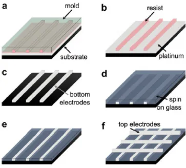
NIL might also be used to realize next generation non-volatile memories. Here, the device structure consists of a resistance switching material sandwiched between two metal nanoelectrodes. Bottom and top electrodes are aligned perpendicular to each other building a crossbar array structure, as indicated in Figure I. 21. A significant advantage of these future devices in addition to their simplicity is the high integration density. Crossbar arrays with 200 nm electrodes and single cross junctions with 30 nm electrodes were achieved using UV NIL. The bottom electrodes were embedded and planarized by spin on glass, such that an even surface for the realization of the top electrodes by UV NIL could be obtained. Finally electrical measurements demonstrated the function of the fabricated devices.
Figure I. 21: Process flow for the realization of crossbar arrays: a: molding, imprinting and UV exposure; b. removing resist residual layer; c. resist etching into platinum layer, giving bottom electrodes; d. surface planarization by spin on glass; e. spin on glass etching till bottom electrodes surface is exposed; f. top electrodes processed in the same way as the bottom electrodes. 59