HAL Id: tel-02613852
https://tel.archives-ouvertes.fr/tel-02613852
Submitted on 20 May 2020HAL is a multi-disciplinary open access L’archive ouverte pluridisciplinaire HAL, est
UV-C light emitting diodes
Alexandra-Madalina Siladie
To cite this version:
Alexandra-Madalina Siladie. AlxGa1-xN and AlN nanowires : a solution for efficient UV-C light emitting diodes. Materials Science [cond-mat.mtrl-sci]. Université Grenoble Alpes, 2019. English. �NNT : 2019GREAY059�. �tel-02613852�
THÈSE
Pour obtenir le grade de
DOCTEUR DE LA COMMUNAUTE UNIVERSITE
GRENOBLE ALPES
Spécialité : Physique de la matière condensée et rayonnement
Arrêté ministériel : 25 mai 2016
Présentée par
Alexandra-Madalina Siladie
Thèse dirigée par Bruno DAUDINet co-dirigée par Julien PERNOT
préparée au sein du Laboratoire PHotonique, ELectronique et
Ingéniérie QuantiqueS (PHELIQS)
dans l'École Doctorale Physique
Nanofils Al
x
Ga
1-x
N et AlN pour la
réalisation de diodes efficaces
émettant dans l’UV-C
Thèse soutenue publiquement le 8 Novembre 2019, devant le jury composé de :
Dr. Bruno DAUDIN
Chercheur, CEA Grenoble, Directeur de thèse Dr. Dr. Lutz GEELHAAR
Chercheur, PDI Berlin, Examinateur Prof. Nicolas GRANDJEAN Professeur, EPFL Lausanne, Rapporteur Prof. Julien PERNOT
Professeur, Université Grenoble Alpes, Co-directeur de thèse Dr. Maxime RICHARD
Chercheur, CNRS Grenoble, Président Dr. Martin STUTZMANN
Chercheur, Walter Schottky Institute and TU Munich, Examinateur Dr. Maria TCHERNYCHEVA
Abstract
Solid-state deep UV Light emitting diodes (LEDs) based on AlxGa1-xN material are nowadays gaining
particular attention due to their potential for replacing mercury lamps, currently used for sterilization and water disinfection applications. However, the realization of planar efficient emitting devices is limited by a high density of extended defects and difficult efficient dopant incorporation affecting both optical and electrical properties. As a strategy to alleviate this difficulty, I have focused on the study of nanowire based heterostructure devices, due to their advantage of elastically relaxing the strain during growth, coupled with a higher dopant solubility limit and an eased light extraction coming from their particular morphology. First, correlated experiments of Atom Probe Tomography (APT), Energy Dispersive X-ray Spectroscopy (EDX) or Raman spectroscopy performed on GaN pn junctions grown by plasma assisted molecular beam epitaxy (PA-MBE) have shown that both n-type and p-type dopants, namely Si and Mg, respectively, exhibit an inhomogeneous radial distribution, with dopant incorporation upper limits attaining 1021 atoms/cm3 at
the periphery, higher than in 2D layers. The study of Mg incorporation by APT concluded on the understanding of the incorporation mechanism, preferential on the m-plane side-wall and assisted by H due to the high stability of the Mg-H complex in N rich conditions.
The second part of the work is dedicated to the study of the more challenging Mg dopant incorporation and activation in AlN alloy, successfully attained in this PhD by In-Mg co-doping. The efficient incorporation of this dopant in AlN nanowires assisted by small concentration of In has been assessed by a series of techniques (EDX, Raman). Ab-initio theoretical calculations have shown that the efficient incorporation of Mg in an Al-substitutional site is due to a process involving the nitrogen vacancies forming an In-VN complex. The formation of AlN NW p-n junction has been concomitantly assessed by electron
beam induced current (EBIC) experiments putting in evidence the electrical field associated with the junction. An extensive study of the electrical activation of acceptor impurities has been further achieved by electron beam irradiation of the samples and characterized in EBIC experiments.
Résumé
Les diodes électroluminescentes (LED) à semi-conducteurs à base de matériau AlxGa1-xN font actuellement
l'objet d'une attention particulière en raison de leur potentiel pour remplacer les lampes à mercure, utilisées pour des applications de stérilisation et de désinfection de l'eau. Cependant, la réalisation de dispositifs émetteurs efficaces en géométrie planaire est limitée par une densité élevée de défauts étendus et par une incorporation des dopants difficile, notamment de type p, ce qui affecte les propriétés optiques et électriques. Pour surmonter ces difficultés, je me suis concentrée sur l’étude des hétérostructures à base de nanofils, en raison de leur capacité à relaxer élastiquement la contrainte pendant la croissance, associée à une limite de solubilité des dopants plus élevée et à une extraction de lumière facilitée par leur morphologie particulière.
En premier lieu, des expériences corrélées de tomographie par sonde atomique (APT), d’analyse dispersive en énergie des rayons X (EDX) ou de spectroscopie Raman effectuées sur des jonctions p-n de GaN développées par épitaxie par jets moléculaires assistée par plasma (PA-MBE) ont montré que les dopants de type n et p, à savoir Si et Mg, respectivement, présentent une distribution radiale non homogène, avec des limites d’incorporation atteignant 1021 atomes/cm3 en périphérie, plus élevées que dans les couches 2D.
L’étude de l’incorporation du Mg par l’APT a permis de comprendre le mécanisme d’incorporation, qui a lieu préférentiellement sur la paroi latérale des nanofils correspondant au plan m et est assistée par l’hydrogène en raison de la grande stabilité du complexe Mg-H dans les conditions de la croissance. La deuxième partie du travail est consacrée à l'étude plus complexe de l'incorporation et de l'activation des dopants Mg dans l'alliage AlN, réalisées dans cette thèse par co-dopage In-Mg. L’incorporation efficace de ce dopant dans des nanofils d’AlN, assistée par une faible concentration d’In, a été évaluée par une série de techniques (EDX, Raman). Les calculs théoriques ab initio ont montré que l’incorporation efficace du Mg dans des sites substitutionnels d’Al est due à un processus impliquant les lacunes d’azote formant un complexe In-VN. La formation d’une jonction p-n dans les nanofils AlN a été évaluée de manière
concomitante par des expériences de courant induit par faisceau d'électrons (EBIC), mettant en évidence le champ électrique associé à la jonction. Une étude approfondie de l'activation électrique des impuretés acceptrices a également été réalisée par irradiation par faisceau d'électrons des échantillons et caractérisée par des expériences EBIC.
Acknowledgements
My PhD was a great collaboration between CEA Grenoble and CNRS-Néel Institute, two of the biggest research centers in France, during which I had the great opportunity of meeting and working with world-renown people in the field of nitrides and semiconductors. Thus, the acknowledgements list will be long and was written in the beginning of my thesis writing journey, because finding words to express my gratitude and support was the easiest task of the process of this PhD manuscript writing. Since the “PhD life” is not just about work, but about personal development, my acknowledgements will be directed towards all of the great people I have met and who have supported me throughout this journey. If I forgot someone, I would like to thank you now.
From a professional point of view, I would like to express my gratitude towards the jury of my PhD defense that I have already had the great opportunity of meeting during several workshops and conferences. I would like to especially thank the reviewers: Dr. Maria Tchernycheva and Prof. Nicolas Grandjean for taking the time to review the partial results of these three years of research. Equally, great thanks to my PhD examination committee, Prof. Martin Stutzmann, Dr. Lutz Geelhaar and Dr. Maxime Richard for accepting to be a part of the jury and examine the PhD defense and the manuscript.
After succeeding in accomplishing one internship and one PhD under his supervision, I would like to thank particularly my PhD director, Bruno. Words cannot express my gratitude towards him and towards the chance he has offered me while accepting me as a part of the team. I am grateful for the endless support and for encouraging me when needed. This continuous “montagne-russe” of PhD ends on a high note thanks to his trust and ambition of always pushing me higher. The scientific discussions we have had will be missed and I hope this will not be our last collaboration.
I have had the chance of having a great working environment and team during my PhD, an equal role for this thesis being played by my co-director, Julien, to whom I am thankful for receiving me in the “diamond group” (even though I was more of a “team GaN” person). I thank him for knowing how to encourage me and for his support and availability every time I needed. I greatly appreciated his understanding as well as optimism when announcing him “unexpected” results. Sitting down with me with nothing but a piece of paper, for hours, trying to understand the physics behind my results, taught me much about his knowledge and I am thankful for the opportunity of having him as a professor and PhD co-director.
Still in the “diamond group” at CNRS, I would like to thank Gwénolé (the other “team GaN” in our wide band gap semiconductors group in Neel Institute). From a more serious point
of view, I would like to thank him for fruitful scientific discussions and a CL efficiency never seen before (even on “unremarkable” samples), as well as for playing an important role in my PhD meetings.
Special thanks to all of my collaborators that were interested in my work and that brought their great knowledge in their respective fields: Fabrice Donatini, for being a part of my scientific group meetings and for his help in EBIC experiments, Ana Cross and Nuria Garro, with whom it was a pleasure collaborating for Raman and KPFM experiments, Lynda Amichi, Bastien Bonef, Adeline Grenier and Catherine Bougerol for results on APT, Yann and Yoann for their technical support and knowledge when MBE was “in trouble”.
Huge thanks to all the great researchers that were a part of the EMOUVAN project: Catherine Bougerol and Jean-Luc Rouvière for the TEM studies, Eric Robin for EDX experiments that always brought great results, Pierre Lefebvre for interesting PL experiments, Mathieu Kociak and Luiz Tizei for nanoscale CL, Damien Caliste and Pascal Pochet for theoretical calculations.
By this mean, I would also like to thank Jean-Michel Gerard for welcoming me in the PHELIQS group at CEA. Also, I would like to especially thank Régis André and Bruno Gayral for welcoming me in the NPSC team and for their great help, support and suggestions while preparing a conference, a regular presentation or even the defense of this PhD (for which I am grateful to Catherine, Fabrice and Gwénolé in an equal measure). I have deeply appreciated the scientific discussions and ideas we have been talking about in order to better orient my PhD. I always knew that despite your (sometimes tough) remarks, the aim of our discussions was to help me reach an exceptional level because of your trust in my abilities.
I have appreciated every minute that I have spent both in CEA and in CNRS. In CEA I have had the chance to be a part of the coffee breaks and to assist to enriching politics, climate, scientific and “team” management debates in the company of Bruno, Regis, Yann, Joel E., Joel B., Samuel, Henri, Eva, Christophe and Yoann. The more organized, “3 times a day” coffee breaks at CNRS were a mean of bringing together all the SC2G team and to have short meetings and discuss about the advancements of the different projects (… but not only). By this mean I would like to thank especially my office colleagues Cédric and Khaled, but also the rest of the SC2G team (and DIAMFAB affiliates) Juliette, Martin, Etienne, Timothée, David, Jesus, Charlotte, Aurelian, Gauthier and Loto.
I have spent most of my PhD time with my CEA colleagues and of course, spending that much time with people must be cherished. I would like to thank Marion, Amine, Akhil, Lynda, Anjali, Akanksha, Romain, Nathaniel, Victor, Rémy, Guillerme, Alexandre, Rodrigo, Caroline, David, Saptarshi, Ioanna, Vincent, Camille, Farsane, Saransh, Sergi, Raouia, Bala, Jane, Matthias,
From a personal point of view, I would like to now thank the people that have supported me during these last 3 years from outside. For this, I thank my best friend Bouchra, for her constant support, as well as my friends from Lyon that are my “Romanian family” in France: thank you Loredana Baboi, Lorena, Sorin and Emily Perisanu, Dana, Lucian and Pierre Roiban. I would like to thank Filippo, Fadoua, Ahlam and Kaoutar, for their friendship and support I have always found in them.
Last but not least, there are always people that come, go and some that stay throughout the years, and that help us become who we are, paving the way towards our future. I would like to express my endless gratitude towards people who encourage us to arrive far even if our paths separate at some point in life. Also, I am extremely grateful towards those people who believed I will go very far in life and helped me attain the confidence and the knowledge I have acquired today: all of my professors, most especially my math teachers, Prof. Steluta Monea and Prof. Lia Vasile.
I will end the acknowledgement list by thanking the most precious people I have in my life, my family, for their constant support and for always being by my side, even in my most difficult decisions:
Vă mulțumesc infinit pentru tot ceea ce ați făcut pentru mine, pentru susținerea și suportul moral pe care l-am găsit mereu în voi. Mulțumesc mami, tati, Buni Cica, Lavi, Ali, bebe Matei, bunici, unchi, mătuși și verișori.
Table of Contents
Acknowledgements ... i
Acronyms ... 5
Introduction ... 7
1. Nitrides for light emission: background and concepts ... 17
III-N material ... 17
Nanowires... 20
General background on III-N material ... 21
1.3.1. Structural properties of III-N material ... 21
Crystal structure ... 21
Polarity... 23
Polarization ... 24
1.3.2. Opto-electrical properties of III-Nitrides ... 25
Electronic transitions and light polarization ... 25
Doping of AlxGa1-xN material ... 28
1.3.2.2.1. n-type doping ... 29
1.3.2.2.2. p-type doping ... 30
1.3.2.2.3. Complexes ... 31
Optical transitions ... 32
Light emitting diodes physics ... 34
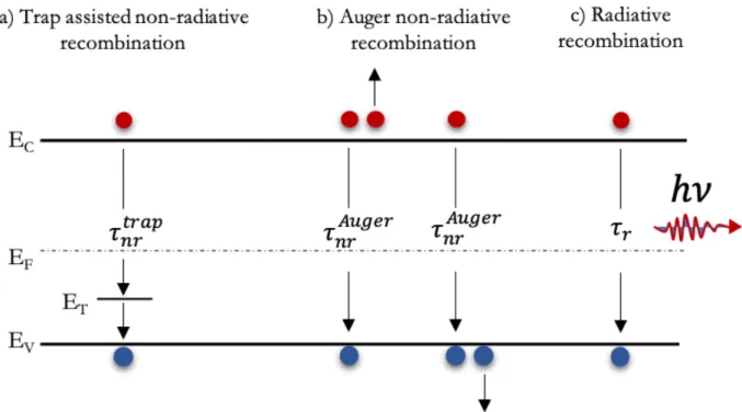
1.4.1. Recombination rate in a semiconductor ... 34
General case ... 34
Nanowires case ... 38
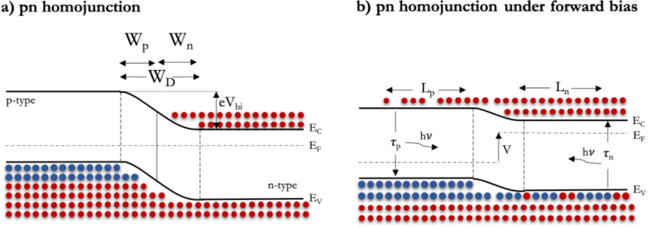
1.4.2. pn junction diodes characteristics ... 39
Ideal diode behavior... 40
1.4.2.1.1. Case of forward bias: ... 40
1.4.2.1.2. Case of reverse bias: ... 41
Real diode behavior... 41
Heterojunctions and carrier confinement ... 43
Nanowire pn junction ... 43
Surface influence on transport properties ... 44
Efficiency and optimization ... 46
1.5.1. External Quantum Efficiency (EQE) ... 46
1.5.2. Carrier Injection Efficiency (EIE) ... 46
1.5.3. Internal Quantum Efficiency (IQE) ... 46
1.5.4. Light Extraction Efficiency (LEE) ... 47
1.5.5. Wall Plug Efficiency (WPE) ... 47
Summary of chapter 1 ... 48
2. Methods and experimental details ... 49
Growth of III-Nitrides ... 49
2.1.1. Epitaxial growth ... 49
2.1.2. Growth techniques ... 50
2.1.3. Description of PA-MBE growth technique... 51
2.1.3.1.1. Pre-growth chamber system... 51
2.1.3.1.2. Growth chamber and vacuum conditions ... 52
2.1.3.1.3. Manipulator and substrate heater ... 52
2.1.3.1.4. Knudsen cells ... 52
2.1.3.1.5. Nitrogen plasma source ... 53
2.1.3.1.6. Reflection High Energy Electron Diffraction ... 53
2.1.4. Growth kinetics mechanism ... 56
Substrate ... 57
2.1.4.1.1. Choice of substrate ... 57
2.1.4.1.2. Substrate preparation... 58
Buffer layer ... 58
Nanowires growth in MBE ... 59
Characterization techniques ... 61
2.2.1. Scanning Electron Microscopy ... 61
Morphology and structural characterization ... 62
2.2.2. Current voltage characterization ... 63
Sample process ... 63
Experimental set-up ... 64
2.2.3. Electron Beam Induced Current technique ... 66
Experimental set-up configuration ... 66
2.2.3.1.1. Preamplification set-up ... 66
2.2.3.1.2. Ammeter set-up ... 67
Quantitative EBIC imaging ... 68
2.2.3.2.1. Injection conditions ... 68
2.2.3.2.2. Experimental fitting of the junction’s parameters... 71
2.2.4. Other techniques and collaboration ... 74
Luminescence experiments ... 74
Energy Dispersive X-Ray Spectroscopy ... 74
Raman spectroscopy ... 75
Atom probe tomography ... 75
Positron annihilation ... 76
Summary of Chapter 2 ... 77
3. Doping problematics in GaN nanowires ... 79
Si and Mg dopant incorporation in GaN... 79
3.1.1. Advantages of nanowire structures ... 81
Si doping of GaN nanowires: inhomogeneous distribution and solubility limit ... 81
Mg-doping of GaN NWs: understanding the incorporation mechanisms ... 82
3.3.1. Atom Probe Tomography analysis ... 82
Samples presentation ... 83
3.3.1.1.1. Growth conditions ... 83
3.3.1.1.2. Nanowires preparation prior to evaporation ... 85
Results: Mg atoms distribution in GaN NWs ... 85
3.3.1.2.1. Atoms distribution analysis in sample #1... 86
3.3.1.2.2. Atoms distribution analysis in sample #2... 89
3.3.2. Mg concentration quantification by EDX ... 91
3.3.3. Raman characterization ... 93
3.3.4. Conclusion ... 95
Vacancy defects study by positron annihilation in doped GaN NWs... 95
3.4.1. Positron annihilation technique ... 95
3.4.2. Samples presentation ... 96
3.5.1. Sample presentation ... 102
3.5.2. EBIC on as-grown sample ... 102
Summary of Chapter 3 ...107
4. Binary AlN NWs: from doping to UV LEDs realization ... 109
AlxGa1-xN nanowire pn junctions for UV-LEDs ...109
4.1.1. Growth conditions of Al0.6Ga0.4N NW sample ... 110
4.1.2. Compositional fluctuations inside Al0.6Ga0.4N NWs ... 111
4.1.3. Optical properties by cathodoluminescence ... 113
4.1.4. EBIC evidence of the pn junction... 114
Sample processing ... 114
Electrical characterization ... 114
Controversial AlN p-type doping issues ... 118
4.2.1. State of the art doping in III-N material ... 118
4.2.2. Growth conditions of AlN NW samples ... 120
4.2.3. EDX-TEM correlated results ... 121
4.2.4. Raman spectroscopy ... 124
4.2.5. Ab-initio co-doping mechanism ... 126
Electrical activation of Mg in AlN doped NWs ...129
4.3.1. Samples presentation ... 129
4.3.2. Optical properties ... 130
4.3.3. Electrical characterization ... 131
4.3.4. Transport properties ... 134
Electrical properties before irradiation: impact ionization in p-type region ... 135
Irradiation impact ... 137
4.3.5. pn junction evidence by EBIC characterization ... 140
Injection conditions ... 140
The irradiation effect on the EBIC profile ... 142
Zero bias pn junction proof by EBIC characterization ... 143
Mg activation by irradiation ... 144
Forward bias effect on an individual nanowire ... 146
4.3.6. Electroluminescence ... 150
Summary of chapter 4 ... 151
General conclusion and perspectives ... 153
Scientific Communications ... 157
Bibliography ... 159
Acronyms
APT Atom Probe Tomography CB Conduction Band
CL Cathodoluminescence DNA Deoxyribonucleic Acid DUV Deep Ultraviolet
EBIC Electron Beam Induced Current EBL Electron Blocking Layer
EDX Energy Dispersive X-Ray Spectroscopy EIE Carrier (electron) Injection Efficiency
EL Electroluminescence
EQE External Quantum Efficiency FIB Focused Ion Beam
HEMT High Electron Mobility Transistors HFET Heterostructure Field Effect Transistor
HR-EDX High Resolution Energy Dispersive X-Ray Spectroscopy HVPE Hydrogen Vapor Phase Epitaxy
IQE Internal Quantum Efficiency ITO Indium Tin Oxide
IV Current versus voltage characteristic
JV Current density versus voltage characteristic KPFM Kelvin Probe Force Microscopy
LED Light Emitting Diode LEE Light Extraction Efficiency LPE Liquid Phase Epitaxy MBE Molecular Beam Epitaxy MOCVD Metal-Organic
NBE Near Band Edge
NH3-MBE Ammonia Molecular Beam Epitaxy NW Nanowire
PA-MBE Plasma Assisted Molecular Beam Epitaxy
PINLED Polarization Induced Nanowire Light Emitting Diodes PVD Physical Vapor Deposition
QCSE Quantum Confined Stark Effect QMAS Quantum MAterials Simulator
QW Quantum Well
RF-MBE Radio Frequency Molecular Beam Epitaxy RHEED Reflection High Energy Electron Diffraction
RS Rock-Salt
SAW Surface Acoustic Wave SCR Space Charge Region
SEM Scanning Electron Microscopy SRH Schokley-Read-Hall
TE Transverse Electric
TEM Transmission Electron Microscopy TM TransverseMagnetic
UHV Ultra-high Vacuum UV Ultraviolet
VB Valence Band VPE Vapor Phase Epitaxy WPE Wall Plug Efficiency
WZ Wurzite ZB Zinc-Blende
Introduction
The 21st century is one of the most beneficial in terms of technological development.
Nowadays, access to high speed internet and high-tech devices is becoming increasingly available. Paradoxically, one third of the global population uses a contaminated drinking water source and almost one billion lack easy access to drinking water, in an era when access to water and sanitation was declared a human right by the United Nations General Assembly (United Nations 2010).
Contaminated water is responsible for transmission of a series of diseases such as diarrhea, cholera, dysentery, hepatitis A. Otherwise preventable and curable, in low-income countries these diseases are still widely spread. In this context, it is crucial to improve water treatment techniques and develop water systems and purifiers.
World Health Organization statistics stress out that by 2025, half of the world’s population will be living in water stressed areas. Increasing water scarcity due to current climate changes and population growth demands strategies such as re-use of wastewater. This justifies the need of intensive research in the water purification domain. Therefore, the development of a highly efficient technique is required (World Health Organization and UNICEF 2017).
However, water treatment is not an anodyne process. Different groups of disease-causing germs have to be considered, such as viruses, bacteria, fungi, algae and protozoa. An affordable and widely-used method for water disinfection is the use of chemical oxidants such as chlorine or ozone, due to their capability for deactivating microorganisms’ DNA (for planktonic bacteria (Bois et al. 1997)) and oxidation (micro pollutants elimination, taste and odor control). Unwanted side effects can be induced during this water treatment, by reaction with water matrix and micro pollutants, leading to unwanted byproducts (Cancho et al. 2000). Moreover, some microorganisms from contaminated water are resistant to a series of chemical oxidants. Therefore, in industrial applications, high-power mercury, deuterium or Xenon lamps are nowadays used, DNA being highly sensitive to UV-radiation.
Ultraviolet light and genetic material
The ultraviolet (UV) light is a band of the electromagnetic spectrum (illustrated in Figure 1a) with wavelength ranging from 10 nm to 400 nm. The UV spectral range can be divided in 4 corresponding regions depending on the wavelength: the vacuum-UV from 10 to 200 nm, UV-C from 200 to 280 nm, UV-B from 280 to 315 nm and UV-A from 315 to 400 nm. The spectral range comprised between 200 and 300 nm will be further referred to as deep ultraviolet or DUV range. Genetic material, more precisely deoxyribonucleic acid (DNA) has an absorption spectrum in the UV-C range. The maximum of the absorption spectrum of nucleic acid and protein varies between 255 and 265 nm (Held 2001; Charak et al. 2012) as shown in Figure 1b.
Figure 1. a) Electromagnetic spectrum with specific ranges. UV-C range is represented in zoom-in view with DNA and protein specific absorbance spectra. b) Optimized absorbance spectra of DNA and protein. c) Illustration of the DNA strand and dimerization of thymine bases under UV-radiation process.
The genetic genome of a DNA is formed from a unique sequence of combined bases amongst adenine, guanine, thymine and cytosine. DNA thymine bases are sensitive to UV-radiation. When exposed to UV-light, bonds between thymine and adenine break and thymine bases are dimerizing and binding together (mechanism illustrated in Figure 1c). When exposed to UV-C light, radiations exert adverse effects on the DNA genome stability. This mechanism affects the DNA strand ability to replicate leading to apoptosis (or programmed cell death), if repairing mechanisms are not efficient enough to counteract the lesions. For this reason, the UV light is known as germicidal beyond a certain dose after which the damage is considered irreversible. This mechanism is responsible for deactivation of genetic material of microorganisms from water and air exposed to a specific radiation wavelength rendering them harmless (Rastogi et al. 2010). The closer the light emitting device to 265 nm wavelength, the better the deactivation efficiency.
The degree of inactivation of the DNA by UV radiation depends on the UV dose and the reduction of microorganisms in water is defined by using a deactivation degree logarithmic scale. Thus, the deactivation percent corresponding to one log reduction or deactivation of microorganisms is 90%, two log reduction is 99% and so on. In order to have a stable and permanent deactivation, 4-log reduction corresponding to 99,99% is needed (Kwok-Keung and LeChevallier 2013), else the genetic material is able to reconstruct the broken bonds and thus lead to an ineffective process. Studies have been carried out on different types of microorganisms and a summary of typical UV fluences required for 4-log inactivation of some of them is given in Table
Table 1. Microorganisms deactivation dose summary
Another important application of UV light is phototherapy for psoriasis disease cure. A narrowband of the UV-B spectra, centered at around 310 nm, was found to lead to apoptosis of a variety of relevant cells in psoriasis such as T-lymphocytes from epidermis and dermis of psoriasis lesions (Ozawa et al. 1999) and keratinocytes (Krueger et al. 1995).
Mercury lamps and regulations
Even if other methods such as chlorine disinfection are equally effective, the UV-radiation process has been found to be extremely efficient with protozoa oocysts and cysts (Hijnen et al. 2006), whereas other techniques are not effective in their elimination.
Current water purification techniques mostly use germicidal ultraviolet lamps produced by using short-wavelength low-pressure mercury vapor tubes that emit at the resonance line of 253.7 nm. Even if this is a widely spread, efficient way of purifying water, mercury, used for manufacturing lamps, is also a very toxic element that presents a series of side effects on human health and environment. This chemical element is widely used in a broad range of everyday products and is released to the atmosphere, soil and water from different sources. While using it as a tool for water purification, it becomes extremely polluting for the environment once it becomes a waste.
Besides the toxic character of mercury, these low-pressure lamps have an efficiency of 30%, demanding a high operating voltage of 100 to 400 V and have low functioning lifetime of between 2,000 up to 10,000 h with a high warm-up period required to reach full light output.
Therefore, the use of these devices and of all mercury-based components will be forbidden starting with 2020, following the Minamata Convention on Mercury treaty signed by the Unites Nations and in place since August 2017 (United Nations 2017). In fifteen years, the extraction of mercury from mercury mines will phase-out and a need for ecologically-friendly and more economically competitive alternative urges.
Sustainable development issues require low energy and low-cost components and devices that deliver high-performances and high-power efficiency. Research centers are investigating the actual need of replacing polluting materials with eco-friendly or less polluting and recyclable alternatives, as well as miniaturization of components and devices, without compromising on efficiency.
Microorganism UV Dose (Fluence) (mJ/cm2)
3-Log reduction 4-Log reduction
Bacillus subtilis (virus) (Sommer et al. 1999) 60 81
Adenovirus (virus) (Thompson et al. 2003) 122 165
Escherichia coli (bacteria) (Wu et al. 2005) 9 10
Salmonella typhimurium (bacteria) (Maya et al. 2003) 22 50
Cryptosporidium parvum (protozoan) (Clancy et al. 2000) 6 16
Al
xGa
1-xN based LEDs as an alternative solution
An efficient solution for satisfying the actual demands would be the production of high efficiency light emitting devices (LED) in the UV-B and UV-C range by using direct band gap semiconductors allowing for an efficient light emission. One option for such devices is the use of the semiconductor alloy AlxGa1-xN that allows for emission wavelength modulation as a function
of aluminum composition. Wide band gap semiconductors with a direct band gap such as GaN and AlN present the advantage of allowing the tuning of the emission in a wide wavelength range. Indeed, AlxGa1-xN material is of high interest in the research community and great progress has
been made in the past years as far as light output power and device efficiency is concerned. The study of its properties is of main importance for this project.
State of the art of Al
xGa
1-xN based UV-LEDs
2D Al
xGa
1-xN based DUV LEDs
Development of AlxGa1-xN based DUV devices and improvement in efficiency are highly
interesting domains for industrial research. Industry groups including RIKEN, Nichia, Nikkiso, LG, Philips or Panasonic have been publishing innovative advances that allow increasing the wall-plug efficiency (WPE) and external quantum efficiency (EQE) of devices. Professor Michael Kneissl from Technische Universität Berlin is summarizing the EQE in DUV LEDs obtained by various research groups throughout the world, as a function of the emission wavelength.
The up to date evolution is shown in Figure 2 (Kneissl et al. 2019). The most important milestones that led to significant efficiency improvement will be further discussed.
Overall, GaN based LEDs show an efficiency as high as 90% for emission wavelengths going from 365 to 400 nm. The discoveries made on GaN blue LEDs have led to Nobel prize accorded to three Japanese researchers in 2014: Professor Isamu Akasaki and Professor Hiroshi Amano from Nagoya University and Professor Shuji Nakamura from Nichia Corporation research center. One of the main difficulties while working with GaN material came from the difficult p-type doping. Their combined research and discoveries on Mg-doping activation by electron beam irradiation in 1989 (Amano et al. 1989; Isamu Akasaki et al. 1991) and by thermal annealing in 1992 (Nakamura et al. 1992b) have led to highly efficient doping in light emitting devices and to the further development of the LEDs used nowadays.
The milestone of the difficulty in doping of III-N materials overpassed, between 1996 and 2001 research has started on AlxGa1-xN-based UV LEDs with wavelengths below 360 nm (Han et
al. 1998; Kinoshita et al. 2000; Nishida et al. 2001). Nevertheless, 20 years later, the external quantum efficiency (EQE) of AlxGa1-xN LEDs is still too low in the 255-265 nm wavelength range
to answer the demands for replacing mercury lamps.
An AlxGa1-xN based LED emitting at 280 nm was reported by a group from University of
South Carolina in 2004 (Sun et al. 2004). First emitting AlN LED done by Tanyiasu et al from Nippon Telephone and Telegraph Corporation (NTT) was published in 2006 in Nature (Taniyasu et al. 2006). The 2D LED was made by using a simple pn junction AlN material and showed emission at 210 nm. The low carrier concentration of p-type AlN was the limiting factor of the efficiency of the diode, due to a high activation energy of Mg acceptors. Nonetheless, the low emission wavelength of the device presented in the paper overpassed an important limit when working with AlN.
The first commercially available LED was developed by Sensor Electronic Technology in 2012. The devices showed emission with wavelengths ranging from 240 to 360 nm and a maximum EQE at 273 nm of 11% (Shatalov et al. 2010, 2012; Mickevičius et al. 2012, 2013; Moe et al. 2012). The internal quantum efficiency (IQE) was improved by growing low density of threading dislocations AlxGa1-xN layers on c-plane sapphire by metal-organic chemical vapor deposition
(MOCVD) as well as UV transparent p-type cladding and contact layers and frontside reflecting ohmic contact.
A record 20.3% for an AlxGa1-xN LED emitting at 275 nm has been presented by Hirayama
et al from RIKEN/Panasonic group. The work was later published in 2017 (Takano et al. 2017). The device’s structure was improved by crystal growth techniques limiting the threading dislocations in 2D AlN grown on a patterned sapphire substrate, allowing an optimized internal reflection of light. The issues caused by low doping in AlxGa1-xN material were suppressed by using
a stack of multiple quantum wells (QW) and an electron blocking layer (EBL) to confine carriers in the QW region, while increasing the electron injection efficiency (EQE). The UV-absorbing top
contact electrode normally done by p-type doped GaN was replaced by a transparent p-AlxGa1-xN
contact layer (Hirayama et al. 2014). Instead of a Ni/Au top metal electrode, a highly reflective photonic crystals contact layer improved the light extraction, considerably.
Nichia Corporation launched in April 2019 their first commercially available UV-C LED emitting at 280 nm in a packaging able to resist significantly harsh environmental conditions (Nichia 2019). Nikkiso and Meiju University have also improved the efficiency of their AlxGa1-xN
based LED’s by introducing a UV-C resisting resin that encapsulates the device. Their emission wavelength ranges between 250 to 280 nm with EQEs higher than 10% (Pernot et al. 2010; Inazu et al. 2011; Yamada et al. 2014).
Diodes grown directly on AlN substrates theoretically yield higher efficiencies than that grown on a foreign substrate such as sapphire or Si. Crystal IS is an American enterprise providing single crystal AlN substrates and have developed LED devices with high lifetime and high light output in the 250-280 nm range, that also present improved thermal performance (Grandusky et al. 2011, 2013).
2D LEDs vs NW LEDs
One promising way in going further with optimization of devices is the use of nanostructures. Nanostructurization of materials eases some of the issues when dealing with AlxGa1-xN material, nanowires (NW) occupying an important place in research. Light extraction
efficiency (LEE) is considerably improved by the use of nanowires. The first 250 nm UV-LED based on semiconductor nanowires was demonstrated in 2013 by a research group at Ohio State University and University of Illinois in Chicago (Carnevale et al. 2013). The team used a radio frequency Molecular Beam Epitaxy (RF-MBE) growth on p-type Si substrate for device fabrication. The use of these nanostructures allowed the compositional variation of AlxGa1-xN in a wide range
without the formation of dislocations from strain relaxation, using the polarization induced nanowire light emitting diodes (PINLEDs). They used the polarization contrast of chemical bonds of differing Al content AlxGa1-xN to reduce the need for p-type doping.
Ultra-low threshold electrically injected AlxGa1-xN nanowire ultraviolet lasers on Si,
operating at low temperature as well as the controlled coalescence of AlxGa1-xN nanowires during
growth to reduce dislocations, and to considerably improve the efficiency of AlxGa1-xN LEDs were
reported by researchers at McGill University in Canada (Li et al. 2015; Le et al. 2016).
As far as NW industry is concerned, no major progress was done in the field of DUV LEDs. CryoNano® is a company based in Trondheim, Norway, founded in 2015, that specializes in nanostructures grown on graphene substrates. However, the LEDs developed so far do not
Path towards improvement of efficiency
Currently, the efficiency of AlxGa1-xN DUV LEDs is still very low compared to that of
standard mercury lamps. The path towards improvement of efficiency is assiduous and innovative ideas have allowed the constant increase of efficiency. Still, the low devices performance is due to mainly three limiting factors:
1. Low hole concentration in p-type AlxGa1-xN caused by a low carrier injection efficiency (EIE);
2. Unsuited metal contact layer and light absorption by p-GaN top contact layer, decreasing the LEE of devices;
3. Low internal quantum efficiency (IQE) due to unsuitable substrate and threading dislocations decreasing the recombination efficiency inside the devices.
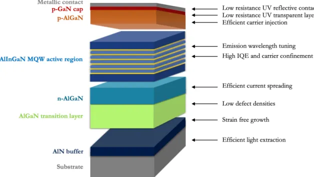
Figure 3. Illustration of the structure of a complete DUV LED device with respective issues associated to each cladding (adapted after (Kneissl et al. 2019)).
Figure 3 illustrates the basic structure of a 2D AlxGa1-xN based UV LED. Even if some of
the above limitations can be more easily overpassed, research is needed to improve some of the issues regarding the carrier concentration in high Al content AlxGa1-xN structures as well as the
metallic top-contacts.
The aim of my PhD was to understand and answer some questions related to physical concepts of nanowire-based UV-LEDs. The research I have done during this PhD concerns AlxGa1-xN NWs, exploring the whole range of Al content (from x=0 in the case of GaN NWs to
x=1 in the case of AlN NWs). My PhD is mainly focused in solving one of the most important problems when dealing with AlxGa1-xN material: the biggest challenge is the control and
characterization of doping in AlN material for further developing pn junctions for LEDs. Following questions were still not answered at the beginning of this project:
o Is the NW doping a specific mechanism?
o How can we incorporate acceptors in AlxGa1-xN and moreover, how can we activate
them?
o How can we measure the activation and doping level?
o What are the transport mechanisms in high Al content and AlN structures? o What other solutions would allow one to improve the metallic contacts for DUV
LEDs?
Organization of the manuscript
Therefore, the manuscript will be divided in four chapters, organized as follows:
Chapter 1 starts with a presentation of the state-of-the-art background and concepts on III-N materials regarding structural, optical and electronic properties necessary for the understanding of future results. The physics behind a pn structure will be developed further, with a special focus on recombination mechanisms.
Chapter 2 presents the methods and experimental details that allowed the development and characterization of AlxGa1-xN UV LEDs. The epitaxial growth technique by molecular beam
epitaxy with the growth mechanisms and sample growth process will be described in the first part of this second chapter. Further, characterization techniques such as Scanning Electron Microscopy (SEM) will be detailed. A full description of experimental set-up for electrical characterization (JV, different configurations for electron-beam induced current-EBIC set-up) will be given, together with theoretical concepts needed for data modelling.
Chapter 3 is focused on GaN nanowires. In particular, we are interested in optimization of p-type doping as well as on explaining the incorporation mechanisms in nanowires. Another interesting part of the study concerns vacancies formation as a function of doping in GaN nanowires. Finally, electrical characterization and EBIC experiments on GaN NW pn junctions have helped us conclude on the importance of studying as-grown nanowires.
Chapter 4 can be divided in two parts: first part is dedicated to the study of AlxGa1-xN NW
compositional fluctuations and on the study of AlxGa1-xN pn junctions by EBIC and electrical
characterization. The second part deals with the study of AlN nanowires. From p-type doping achieved by In-Mg co-doping mechanisms, to AlN pn junctions, we have improved the feasibility of AlN based LEDs. Irradiation has shown an important effect on Mg activation in the pn -junctions. Electrical transport properties were studied in detail and transport mechanisms were
04, EMOUVAN project. Most of the research was done at the Atomic Energy and Alternative Energies Commission (CEA), but also at the National Center for Scientific Research (CNRS)-Neel Institute in Grenoble, France.
Concerning my contribution to the project, my work was divided between the two laboratories I was a part of:
At CEA Grenoble, I was in charge of the growth of the samples by Molecular Beam Epitaxy (MBE), as well as of the structural characterization by Scanning Electron Microscopy (SEM) and preparation of the samples (identification of the region of interest for different studies, dispersion, annealing, etc…) under the supervision of my PhD director Dr. Bruno Daudin. Regarding the organization of the project, I was in charge of the collaborations by defining the various complementary studies, interacted with the different collaborators and I gathered and participated at the interpretation of results.
The work at CNRS Grenoble was centered around the electrical characterization of the samples: from clean room processing of the samples (electrodes conception, metal and ITO sputtering, annealing) to IV experiments. Electron Beam Induced Current (EBIC) is one of the major techniques I have used for the study of the electrical properties of AlxGa1-xN materials, under
the supervision of my PhD co-director Prof. Julien Pernot.
A big part of the manuscript is dedicated to the doping and study of electrical properties, since my PhD was focused on the growth and optimization of structures for future DUV LED devices. Answering a part of these questions would not be have been possible without the numerous collaborations I have had during these three years:
• Cathodoluminescence experiments have been performed by Dr. Gwénolé Jacopin at CNRS-Neel Institute- in Grenoble;
• Energy Dispersive X-Ray (EDX)-TEM correlated experiments have been done by Dr. Eric Robin at CEA- INAC in Grenoble;
• Raman Spectroscopy experiments were performed by Dr. Ana Cros and Dr. Nuria Garro at the Materials Science Institute at University of Valencia in Spain;
• Theoretical and ab-initio calculations were done by Dr. Damien Caliste and Dr. Pascal Pochet at CEA Grenoble;
• Atom Probe Tomography experiments were done during the PhD of Lynda Amichi and under the supervision of Dr. Catherine Bougerol and Dr. Adeline Grenier at CEA Grenoble.
• Positron annihilation experiments were performed by Prof. Akira UEDONO from the University of Tsukuba, Japan.
1. Nitrides for light emission:
background and concepts
After introducing the motivations for replacing mercury lamps by AlxGa1-xN based LEDs,
we will focus in this chapter on describing the particular properties of this direct band gap semiconductor that make it an outstanding candidate for DUV LEDs development.
III-N material
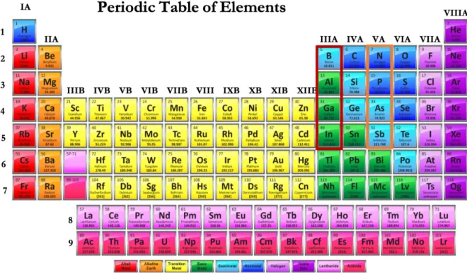
III-V materials define an alloy formed by a third (IIIA) column element (B, Al, In, Ga) and a fifth (VA) column element (N, P, As) (see Figure 4). BN, AlN, GaN and InN are the four main III-N materials exhibiting outstanding optoelectronic properties, which make them suitable for integrating different semiconductor application domains. AlN, GaN and InN materials exhibit similar properties and are considered as “standard nitrides”, whereas BN material exhibits very peculiar opto-electronic and structural properties and will not be concerned in the following.
Figure 4. Periodic table of elements evidencing the 3rd and 5th column elements forming the III-V materials category
Figure 5. Band gap energy (Eg) variation of the technologically important III-V binary materials with respect to the
lattice parameter (in-plane lattice parameter in the case of wurzite nitrides). Image from reference (Caro Bayo 2013)
The emission wavelength and band gap energy (Eg) dependence on lattice parameters for
group III-V semiconductor materials is illustrated in Figure 5 (Caro Bayo 2013). The standard nitrides we are interested in have a band gap at room temperature equal to 0.78 eV (near IR) for InN, 3.51 eV (near UV) for GaN and 6.25 eV (extreme UV) for AlN. We will be mostly focusing on the properties of AlN and GaN binary alloys for DUV emission, InxGa1-xN being an ideal candidate
for visible light emission. Therefore, the interest for DUV LEDs based on wide direct band gap semiconductors comes from the possibility of tuning of the emission in a wide wavelength range, from 200 to 365 nm, with both p-type and n-type conductivities in the UV range.
Hence, in order to cover the entire spectral range, intermediate ternary alloys such as AlxGa1-xN, where x is the Al fraction, are synthesized by combining binary alloys. Generally, the
band gap energy of an AxB1-xN alloy for a given composition is given by the empirical equations
determined from Vegard’s law:
"#$%&'(%) = +"#,-+ (1 − +)"
#3-− +(1 − +)4 (1)
Where b is the bowing coefficient that corrects the simple linear relation involving the A and B species. For AlxGa1-xN, this empirical parameter is ranging between 0.53 eV and 1.3 eV
with customizable wavelength as a function of their composition. Moreover, AlxGa1-xN is of high
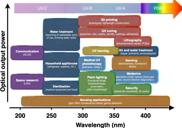
interest in the research community due to the large lifetime of electrical devices and physical hardness. The targeted lifetime of UV LEDs is expected to be of the order of 20,000 hours, 10 times higher than that of UV lamps, with no warm-up time, allowing to reduce the total costs of devices thanks to savings on power supply and packaging costs. On the other hand, the small spot sizes of the surfaces to be illuminated is a disadvantage with respect to large mercury lamps (Kneissl and Rass 2016; Kneissl et al. 2019).
Figure 6. Light output power of UV-LED applications based on AlxGa1-xN classified with respect to the emission
wavelength (image adapted from (Kneissl and Rass 2016)).
In UV-C range, one of the most important application domains is the sterilization of food and medical equipment as well as the water purification, as described previously. At the higher wavelength of 300 nm, AlxGa1-xN is used for plant lighting in agriculture as well as for medical
purposes such as for UV-curing of psoriasis and vitiligo disease. Besides LEDs, more general uses of III-N materials in the optoelectronic field include lasers for applications such as DVD Blue-ray readers (Figure 6). Amongst the general application of III-nitrides we can also mention high power and high frequency electronics such as Heterostructure Field Effect Transistors (HFET) or High Electron Mobility Transistors (HEMT). AlN based devices are used for Surface Acoustic Wave (SAW) devices, signal treatment or for touchscreens in mobile applications because of their piezoelectric properties (Kneissl and Rass 2016).
Nanowires
The requirement for improved efficiency of actual devices could benefit from the use of nanowire heterostructures. Semiconducting nanowires are one-dimensional nanostructures having a diameter of around 100 nm and a height over diameter ratio higher than 10 (Rigutti 2015). The term “nanowire” has been extended to nanostructures exceeding 100 nm diameter, going up to several micrometers, nevertheless, the term “microwire” is more adapted to define this kind of structures. For structures for which the height over diameter ratio is lower than 10, the common terms “nanorod” or “nanocolumn” is employed.
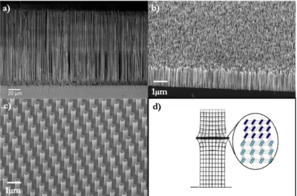
Figure 7. SEM images for GaN nanowires synthesized by different techniques. a) MOCVD (El Kacimi et al. 2018) b) MBE (this work) c) MOCVD by using selective area growth method (Aledia 2019). d) Strain relaxation mechanism on the lateral walls of a nanowire adapted from (Niquet et al. 1997).
Different examples of nanowires synthesized by different techniques are presented in Figure 7a, b and c. The main interest of these nanostructures comes from the high surface to volume ratio that favors surface effects. Elastic strain relaxation during growth considerably reduces the crystallographic extended defects rising from lattice mismatch between materials. Because of the unique boundary conditions, nanowire heterostructures are more effective in relieving mismatch strain coherently, exhibiting defect-free interfaces (Niquet et al. 1997). The crystal quality in nanostructures is also considerably improved because of the small diameter allowing strain to be relaxed laterally, whereas in planar layers the strain could be relaxed only along one dimension (Ertekin et al. 2005).
A critical layer thickness below which no interfacial dislocation should be introduced was determined in literature by evaluating the elastic energy stored in systems (Yoshizawa et al. 1997). Efficient dopant incorporation in nanowires is also worth mentioning as an advantage of studying
General background on III-N material
The properties of III-N standard materials are similar regarding crystal structure, polarization effects or defects. Therefore, while presenting the state of the art and general properties, I will be talking mainly about AlxGa1-xN material (from which one understands AlN,
GaN as well as the AlxGa1-xN alloys).
1.3.1. Structural properties of III-N material
Crystal structure
Depending on the growth parameters, the III-Nitride semiconductors as well as their ternary alloys such as AlxGa1-xN, exhibit three different crystalline arrangements:
Figure 8. Crystal structure of III-N materials: a) Wurzite, b) Zinc-blende, c) Rocksalt structure d) Plane staking in wurzite structure, e) Plane stacking in zinc-blende structure. Nitrogen atoms are represented in green and metal atoms in blue.
• Wurzite (WZ): or w-phase structure illustrated in Figure 8a belongs to the P63mc
space group and has an ABAB atomic layer hexagonal stacking pattern, where A and B refer to different in-plane positions of the III-N atoms (Figure 8d). Its primitive unit cell is composed of two hexagonal close-packed sub lattices formed by two metal and two nitrogen atoms. Those sub lattices are shifted one with respect to the other along the [0001] direction (further defined as c⃗) by a vector u8⃗ = 3c⃗ with respect to the ideal structure (which can be seen as a tetrahedron where each metallic element is bonded to four N atoms and vice-versa). This is the main phase seen in the samples grown during the PhD.
• Zinc-blende (ZB): cubic or c-phase structure belonging to the F4̅3m space group is
C plane rotated by 60° with respect to A, in the [111] direction. The unit cell is constituted of two face centered cubic lattices shifted by √3a in the [111] direction. This phase is thermodynamically less stable than the wurzite phase. However, it is possible to obtain it by controlling the growth parameters, for example using a cubic substrate such as 3C-SiC (Okumura et al. 1994, 1997; Wei et al. 2000) or GaAs (Okumura et al. 1991; Lin et al. 1993), or by decreasing the growth temperature, introducing stacking faults in the wurzite segments (Daudin et al. 1998; Hestroffer 2012).
• Rock salt (RS): structure presented in Figure 8c belongs to Fm3>m space group and the unit cell can be considered as a face-centered cubic structure with secondary atoms in the octahedral holes. This phase can be synthesized only under extreme growth conditions that imply growth at very high pressure, incompatible with MBE growth technique (Christensen and Gorczyca 1994).
Figure 9. Crystal planes in wurzite lattice structure.
The most common crystallographic structure due to its thermodynamic stability is wurzite. The nanowires grown during this work only show this crystallographic structure. Different crystallographic planes of the hexagonal wurzite lattice are represented in Figure 9 and the description is given in the four indices base notation (h k i l) specific to hexagonal structure. The h, k and l indices are the Miller indices whereas the i parameter is defined as i=-(h+k). This notation allows an easy identification of equivalent planes thanks to indices permutations.
The wurzite lattice structure is defined by 2 main parameters, the length a of the hexagonal base and the height c of the lattice, as represented in Figure 8a. Table 2 gives a and c parameters for GaN, AlN and InN at room temperature (300K) and atmospheric pressure (Vurgaftman and Meyer 2003).
Lattice parameters GaN AlN InN
Polarity
One particularity of the wurzite crystal structure is the lack of centro-symmetry, due to the presence of a unique polar axis collinear to the c⃗ axis. Hence, the [0001] (C) and
[0001>] (−C) directions are not equivalent (Hellman 1998). A convention has been adopted to define the polarity of the III-N crystal: the positive direction of the c⃗ axis [0001] is the vector going from the metallic atom and pointing towards N in the direction of the metal-nitrogen bond, which is collinear to the c⃗ axis of the wurzite cell.
Figure 10. a) metal-polar structure and b) N-polar structure.
The wurzite unit cell and the equivalent directions are illustrated in Figure 10. The growth usually takes place along c⃗ direction, so the nanostructure or layer polarity is defined by the +c or
-c dire-ction, defining also the polarity of the -crystal.
Metal-polar: a structure is said to be metal-polar when its growth direction is c, with a Ga-N bond directed towards the surface, oriented from a Ga or Al atom towards an Ga-N atom.
N-polar: a structure is said to be nitrogen-polar when its growth direction is -c, with a Ga-N bond oriented from a Ga-N atom towards Ga or Al atom.
The control of polarity is important when working with III-N nanowires, since optical, electrical and morphological properties are depending on it. There are several ways of establishing the polarity of AlxGa1-xN material, such as the widely used chemical etching by KOH, X-ray
diffraction (Hestroffer et al. 2011), KPFM (Minj et al. 2015) or Convergent Beam Electron Diffraction (Largeau et al. 2012).
Polarization
A consequence coming from the WZ symmetry is the presence of a macroscopic spontaneous polarization called DEF. The difference between nitrogen and metal atoms, where N
atoms have a smaller atomic radius and a higher electronegativity than metal atoms, forms an electrostatic dipole, with negative charges towards N and positive charges towards the metal. Since the -c and c orientations are not equivalent, the charge distribution forms a polarization field DEF
along the c⃗-axis. Conventionally, the DEF vector is oriented (along the c⃗ axis), from the N atom
toward the metal atom, independent of the crystal polarity.
While applying an external force to a III-N material, an additional piezoelectric polarization (DFG ) dependent on the crystal polarity has to be considered. Since N atom is more electronegative
than metal atoms, crystals’ atomic positions are modified by stress and lead to a different spatial distribution of the negative and positive charges, inducing a piezoelectric polarization. This additional polarization is negative on the metal side and positive on the N side. The total polarization DHIH in the nanostructure is the sum of the two previous polarizations (DHIH= DEF+DFG)
induced by strain into the band structure during growth.
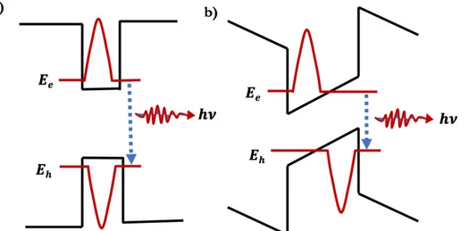
Figure 11. QCSE and wavefunction in AlxGa1-xN/GaN active region with a) no electric field and b) with electric
field.
A direct consequence is the recovering domain for wave functions for the conduction band and for valence band. This limits the efficient radiative recombination probability of electrons and holes, decreasing the optical emission. The phenomenon is known as Quantum Confined Stark Effect (QCSE). Figure 11 illustrates the wave functions of a quantum well under no electric field (a) and under the perturbative effect of an external electric field (b). Undesired effects such as incorporation rate of extra atoms for doping and alloying (Duff et al. 2014) or incorporation of defects (Schuck et al. 2001) can be equally observed.
1.3.2. Opto-electrical properties of III-Nitrides
Electronic transitions and light polarization
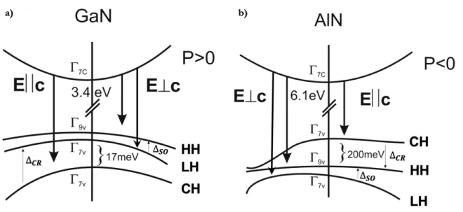
Being direct band gap semiconductors, the opto-electrical properties of III-N materials are determined by the band structure near the Brillouin zone center at the wavevector J8⃗ = 08⃗, represented as the Γ point. The minima of the conduction band and the maxima of the valence band are both in the Γ point.Figure 12. Band structure and transitions for a) WZ GaN and b) WZ AlN (adapted from (Kneissl and Rass 2016))
Both AlN and GaN have one unique conduction band (CB-ΓLM) with atomic s-orbital states.
However, the valence band (VB) presents a three-level degeneracy (Suzuki et al. 1995). First, due to the asymmetry of the crystal, a partial degeneracy occurs because of the interaction with the crystalline field (of energy ∆OP). Second, the spin-orbit interaction determines an additional
degeneracy of the valence band (of energy ∆QR). The valence band is thus formed by a heavy-hole
band (HH- ΓST), a light-hole band (LH- ΓLT) and a spin-off band (CH- ΓLT) represented in Figure
12 for GaN and AlN, respectively.
The valence band (VB) is divided in px, py and pz states, depending on the axis of the crystal.
The z direction of the orbital state is defined being the axis parallel to the c-axis of the crystal, whereas x and y are perpendicular to this direction and to each other.
There are three possible electronic transitions resulting from recombination of an electron excited into the conduction band and a hole in the valence band coming from s states and p states. The polarization of light resulting from these recombinations depends on the direction of the p orbital states. The light resulted from transitions between orbital states parallel to the c direction is called TM polarized (transverse magnetic), whereas light coming from recombination between the conduction band and the holes in the top-most valence band perpendicular to the c direction is called TE polarized (transverse electric).
The three valence sub-bands are different for AlN and GaN due to the crystal field splitting. For AlN, the top-most band is the CH, followed by the HH and LH band, whereas for GaN, the HH is the lowest energy sub-band, followed by LH and CH (Chen et al. 1996). The transitions in the two crystals between the valence sub-bands and the conduction band are thus not equivalent. Since lower band gap energies are more favorable than other transitions, photons give the maximum luminescence intensity for TM polarized light for AlN (Li et al. 2003), while for GaN it is strongly TE polarized (Chen et al. 1996).
A direct consequence of the different light polarizations is that when working with an alloy, the choice of structure of a LED device should be adapted for an optimized light extraction. The degree of polarization of light emitted from the ternary AlxGa1-xN alloy is directly related to the
composition (Coughlan et al. 2015). Depending on the AlN content, light emitted from a 2D UV LED structure grown along the c-axis can switch from TE polarized to TM polarized, which is an important factor for light extraction from the structure (Kneissl and Rass 2016).
Therefore, light loss is one of the major factors limiting the device efficiency. Depending on the design of the structures, light will be partially reabsorbed in the device, another difficulty arising from extraction efficiency. The AlN material case is even more challenging, since the TM polarized light is in the plane of the structure, favoring extraction through the sides. During this process, the light is partially reflected and re-absorbed in the structure, resulting in poor device performance.
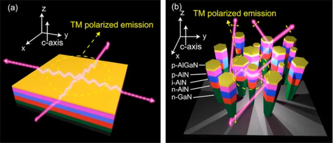
Figure 13. Light emission from a a)2D AlN LED and b) NW-based AlN LED (Zhao et al. 2015c).
Figure 13 illustrates the TM polarized light emission coming from a 2D AlN LED and that coming from a NW based AlN LED (Zhao et al. 2015c). While dealing with nanostructures, this inconvenience is no more a challenge, since light extraction is eased in all directions of the device.
acoustic and optical phonons, showing the occupation of these phonon levels.
The values of band structure parameters for GaN, InN and AlN are summarized in Table 3 (Vurgaftman and Meyer 2003):
Table 3. Band structure parameters for GaN, AlN and InN
The decrease in the gap energy with temperature of the order of ~100 meV is related to the electron-phonon coupling, according to the Varshini model ( Levinshtein, Rumyantsev, and Shur 2001) by the relationship below:
"#(U) = "#(0V) − W ∙ UY
Z + U (2)
With W and Z Varshni’s thermal coefficients given in Table 4 (Vurgaftman and Meyer 2003).
Table 4. Varshini thermal coefficients for GaN, AlN and InN
GaN AlN InN
"# ([\) 3.510 6.25 0.78
∆
SO(][\) 17 19 5
∆ ^_ (][\) 10 -169 40
GaN AlN InN
α (`ab. def) 0.909 1.799 0.245
Doping of Al
xGa
1-xN material
Besides the three electronic transitions defined above, the electron-hole pairs may interact with structural defects and non-ionized impurities in the III-N material, bounding to the latter. These impurities have a different electronic configuration than the intrinsic nitride material, introducing additional energy levels in the band gap. Substitutional impurities and point-defect associated levels can be either close to the conduction band, in which case the impurities behave like donors, or to the valence band, behaving as acceptors. Depending on the position in the band gap, these levels are defined as “shallow” if they are close to either the valence or the conduction band, or “deep” if they are located around the middle of the band gap.
Physical and electrical properties of semiconductor materials are highly influenced by the presence of defects, intentionally or unintentionally created. Defects such as stacking faults, dislocations or point defects are introduced during growth in the material, when growth conditions are not optimized. In LEDs, such defects are mainly responsible for poor performances of the devices, since they are non-radiative recombination centers trapping carriers before recombination (Sugahara et al. 1998).
The main point defects are native defects, impurities, and complexes with the size comparable to the nearest atomic distance. In III-N materials, the most important ones are group II impurities (Zn and Mg), as well as C, Si, H, O, Be, Mn, Cd (Reshchikov and Morkoç 2005). Native defects affect the electrical and optical properties of semiconductors by introducing numerous energy levels in the gap. Usually, this type of impurities is a result of non-stoichiometric growth or annealing, being formed as compensation sources when dopants are introduced. Vacancies, interstitials and anti-sites are isolated native defects, their interaction forming a complex. Their probability of appearing highly depends on their formation energies. Defects with high formation energies such as self-interstitials and anti-sites are unlikely to occur in GaN during growth, however electron irradiation or ion implantation can highly increase their creation probability. Also, Ga vacancies generally occur in n-type AlxGa1-xN whereas N vacancies are more
likely in p-type AlxGa1-xN (Neugebauer and Van de Walle 1999).
Depending on their electronic configuration and whether they have more or less electrons than the species forming the crystal, impurities in III-N semiconductors are considered as shallow donors or acceptors. Complexes between native defects and impurities introduced unintentionally are usually the dominant type of defects in III-N materials (Mattila and Nieminen 1997; Van de Walle 1997; Van de Walle and Neugebauer 2004).
Physical properties of semiconductor materials such as conductivity, band gap energy or charge carriers are mainly governed by doping. Tuning the electrical conductivity and elaboration
1.3.2.2.1. n-type doping
To obtain n-type doping of AlxGa1-xN material, elements from the fourth or sixth column
elements of the periodic table are used. C, Si, and Ge on the Ga sites (Figure 14) and sixth column elements such as O, S, and Se on the N sites are considered as shallow donors in GaN (Reshchikov and Morkoç 2005). However, in order to become an electrically active donor of the material under consideration and participate to conduction mechanisms, the charge carriers have to be ionized requiring an ionization energy Ea.
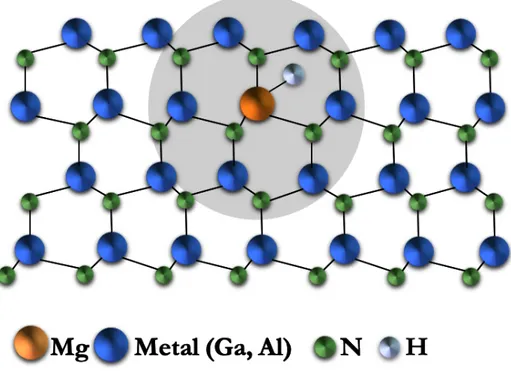
Figure 14. Si atom in substitutional metallic site in AlxGa1-xN crystal lattice and Fermi level position close to the
conduction band for a n-type doped material.
Various studies have determined the ionization energies of impurities for GaN wurzite (Reshchikov and Morkoç 2005). The donor ionization energies in wurtzite GaN are 34.0, 30.8, and 31.1 meV for C, Si, and Ge on the Ga site, and 32.4, 29.5, and 29.5 meV for O, S, and Se on the N sites (Wang and Chen 2000).
In AlN, the same donors present much higher ionization energy. Si is a native donor of AlN with an ionization energy as high as 282 meV (Taniyasu et al. 2006). C in Al site ionization energy is of 200 meV (Lyons et al. 2014). In III-N materials, the metal vacancy is the main defect, substitution of metal atoms from the III-N lattice by fourth column elements being easier than that of nitrogen atoms. The two main candidates for n-type conductivity are Si and Ge. The use of Ge as a n-type dopant of GaN material increased during the last years (Nakamura et al. 1992a; Dadgar et al. 2011; Fritze et al. 2012; Hille et al. 2014; Beeler et al. 2014; Ajay et al. 2017). However, in AlxGa1-xN materials, clustering of Ge dopants for Al content higher than 0.4 together with a low
donor activation has been observed (Ajay 2018). Even though Si and Ge present relatively close activation energies, the small radius of Si as well as the great availability makes it the dominant candidate for AlN and GaN materials. Since in AlN material the Si activation energy is higher than in GaN, the doping activation is expected to be more challenging, with formation of localized deep states (Bremser et al. 1998). In consequence, in AlxGa1-xN alloys, the Si donor ionization energy
increases from 30 meV to 282 meV, depending on the Al content. Increase in Al composition is also accompanied by the increase in the density of defects with energy levels deeper than Si. Combined action of the two above effects leads to the rather challenging n-type doping of AlN material.