HAL Id: hal-01895805
https://hal.archives-ouvertes.fr/hal-01895805
Submitted on 15 Oct 2018
HAL is a multi-disciplinary open access
archive for the deposit and dissemination of
sci-entific research documents, whether they are
pub-lished or not. The documents may come from
teaching and research institutions in France or
abroad, or from public or private research centers.
L’archive ouverte pluridisciplinaire HAL, est
destinée au dépôt et à la diffusion de documents
scientifiques de niveau recherche, publiés ou non,
émanant des établissements d’enseignement et de
recherche français ou étrangers, des laboratoires
publics ou privés.
Packaging with double-side cooling capability for SiC
devices, based on silver sintering
Cyril Buttay, Raphaël Riva, Bruno Allard, Marie-Laure Locatelli, Vincent
Bley
To cite this version:
Cyril Buttay, Raphaël Riva, Bruno Allard, Marie-Laure Locatelli, Vincent Bley. Packaging with
double-side cooling capability for SiC devices, based on silver sintering. 44th IEEE IECON, IEEE,
Oct 2018, Washington DC, United States. �10.1109/IECON.2018.8591117�. �hal-01895805�
Packaging with double-side cooling capability for
SiC devices, based on silver sintering
Cyril Buttay, Rapha¨el R
IVA, Bruno Allard
Universit´e de Lyon,
INSA-Lyon, Universit´e Claude Bernard Lyon 1, ´
Ecole Centrale de Lyon, CNRS Amp`ere, F-69621 Villeurbanne, France
Marie-Laure Locatelli, Vincent Bley
Universit´e de Toulouse UPS, INPT, CNRS LAPLACE F-31062
Toulouse, France
Abstract—Although they can operate at high temperature, SiC devices require efficient thermal management. One solution is to use a dual-side cooling packaging, where heat can be extracted through two surfaces. Here, such a package is presented, using only materials which can operate at high temperature (>200°C): ceramic substrates, silver sintering, fluorinated parylene. Due to the small feature size of the SiC dies used, a special care is given on the etching resolution of the substrates. The complete manufacturing process is presented, and some characterization results are given to demonstrate that the package is operational.
I. INTRODUCTION
Silicon-Carbide (SiC) power semiconductor devices are especially suited to high temperature operation (>200 °C). In particular, Junction Field Effect Transistors (JFETs) can oper-ate reliably at elevoper-ated temperature [1], [2], because they do not suffer from gate oxide issues. High-temperature capability is desirable for applications such as aerospace (especially near the jet engine or the brakes of an aircraft), oil and gas drilling, or automotive [3], where the devices may operate in harsh ambient conditions.
However, despite their inherent capability to operate at high temperature, which originates from the large energy band-gap of SiC [4], SiC JFETs are prone to thermal runaway [5] (this would also be true of other unipolar devices such as Schottky diodes [6] or MOSFETs): as their on-state resistance (RDSon)
increases strongly with the temperature (RDSon ∝ T2.4 or
more [7]), so do their losses. If insufficient cooling is provided to the JFET, this yields to a race condition in which increasing losses result in ever higher junction temperature. This is known as thermal runaway, and usually results in the destruction of the device.
As a consequence, these devices must be attached to an efficient thermal management system: thermal resistances of around 1 K/W are required [7], even though the temperature of the ambient air surrounding the converter can be as high as 200 °C or more.
One limitation of standard packaging solutions is that cooling is provided through one side of the dies only. Many research groups have proposed improved packaging struc-ture [8], [9], and some of them provide double-side cool-ing [10]. In most cases, these power modules have the
so-called “sandwich structure”, where the dies are placed between two ceramic substrates, which provide both thermal conduc-tion and electrical insulaconduc-tion. This is the case of the modules presented in [11], [12], [13], [14]. In some other cases, a single ceramic substrate is used, and electrical isolation is provided through one side only [15], although heat can be extracted through both sides of the package.
An important issue in these packages is to provide some spacing between the topside of the power dies and the upper substrate: a direct contact with the flat metal layer of the substrates would cause a short circuit of the edge protection features on the dies. As a consequence, different solutions were proposed, for example using small cylinders to connect the dies and the upper substrate [11], [12], or a single, massive spacer [14]. Another solution, which is also used in this paper, is to form protruding features on the metal layer of the substrate [13].
Most of the structures proposed so far are based on solder interconnects. This is a very mature technology, but is not so well suited to high temperature operation [16]. Among the die attach solutions that can be used at high temperature [17], [18], silver sintering [20] is especially attractive. This solid-state process can be performed at a temperature of 240 °C, but the resulting die attach (pure silver), can operate reliably at higher temperature (for example 300 °C in [19]).
Most of the research on silver sintering focuses on backside die attach, but some papers investigate topside contact: in [21], a ribbon is attached using silver sintering, as a replacement for aluminium wire-bonds; in [22], dies are attached on both sides using silver sintering, with the topside interconnect provided by a flex circuit. In [23], a sandwich structure is assembled using (gold) sintering, but no details are given regarding the high voltage capability of the package: apparently, flat ceramic substrates are used, without any spacer. As a consequence, the topside of the dies is very close to the metal layer of the substrate. Finally, a sandwich structure is assembled using silver sintering in [24], and shows good voltage blocking capability (switching tests performed at 750 V). Unfortunately, the topside interconnection of the dies is not detailed.
As described above, some spacing is required between the edge protection of the dies and the surrounding metal layer, so
Fig. 1. 3-D view of the power module, showing the 2 SiC JFETs, and the internal routing.
Fig. 2. Topside layout of the two JFET variants used in the module. Left: 4×4 mm2 die, right 2.4×2.4 mm2. Both have the gate pad in the centre of the die, surrounded by the source contact. Topside metal is aluminium.
that the blocking voltage capability of the dies is maintained once packaged. For the same purpose, a suitable encapsulation of the dies is also required [25], as the voltage breakdown of air is not sufficient. Classically, Silicone gels and epoxy resins are used for this purpose. Both have been successfully used in sandwich packages ([13], [14] respectively). Most of these materials are not suited to high temperature operation, though, as they degrade rapidly (a few days at 250 °C, [26]). Other materials can operate at a higher temperature, or for a longer time: polyimides [26], [27], and parylene HT [27], [28]. This is the later solution that was selected for the module presented here, and it is described in the article. Indeed, silver migration [29], one of the issues associated with high temperature operation of silver sintered joints, was found to be clearly reduced using parylene encapsulation [28], [30].
In the next section, we present the concept of the sandwich package. Section III describes the manufacturing process. Evaluation results are presented and discussed in section IV.
II. DESIGN OF THE POWER MODULE
A 3-D view of the power module is visible in figure 1. It comprises two SiC JFETs (SiCED, now Infineon) and two ceramic tiles. Two variants of the SiC JFET were used, and their layouts are presented in figure 2: the 4×4 mm2 version has a 60mΩ on-state resistance, while that of the smaller (and older) 2.4×2.4 mm2 version is 500 mΩ. Both dies are rated at 1200 V, and were successfully tested at temperatures
SiC JFET Alumina 0.2 mm 0,3 mm 0.16 mm 0,15 mm Copper
0.15 mm Source Gate Source
Drain
0.3 mm
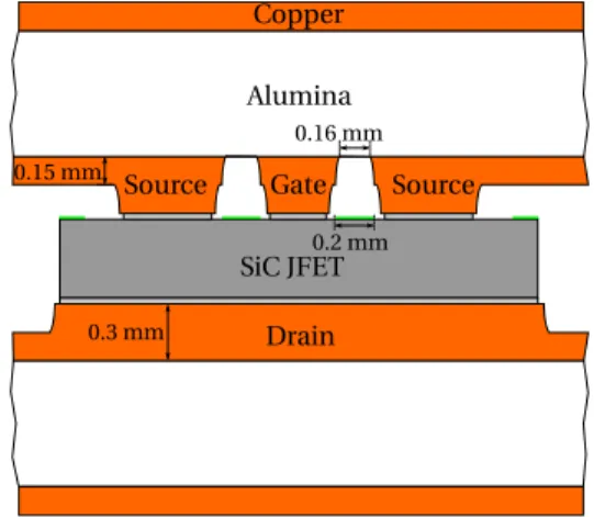
Fig. 3. Cross section of die interconnects (scale view, for a 2.4×2.4 mm2 die). The JFETs considered have a small gate contact in the centre of the die, surrounded by the source pad. Protruding features are necessary on upper DBC to prevent shortening the edge protections of the die.
exceeding 300 °C. From a packaging point-of-view, these devices have the source and gate pads on the topside of the die, and the drain on the bottom-side. The gate pad is fairly small (0.35 by 0.56 mm or 0.41 by 0.86 mm).
A close-up view of the interconnects to be realized is visible in Fig. 3. It shows that in order to provide both gate and source contacts without creating any short circuit between these pads, and to avoid touching the edge protections of the die, a two-level copper layer is necessary: protruding features form the actual contact with the die, while the thinner areas are used to route the electrical circuit. The small sizes of the die and of its gate pad require a “high resolution” etching of the copper (0.2 mm spacing for 0.3 mm-thick copper conductors). The etching technique, which is not compatible with the guidelines of the industry [31], is described in section III. For high-temperature operation, an attractive ceramic material is Silicon Nitride (Si3N4) [25], [18]: it offers good insulating properties,
even at elevated temperatures, and better mechanical strength than the other ceramic materials (alumina and aluminium nitride). This latter point is important to survive the large tem-perature swing associated with high temtem-perature applications. However, due to cost considerations, alumina Direct Bonded Copper (DBC) substrates were used during the work presented in this article.
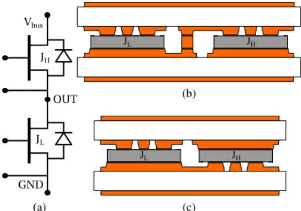
The module forms a half-bridge circuit, as depicted in Fig. 4a. An arbitrary design choice is to give both JFETs the same orientation (i.e. to have their gate and source pads contacting the same DBC tile of the sandwich structure, Fig. 4b). This makes it necessary to provide a direct contact between both tiles. The advantages of this organization is to have all the control connections on one tile, and the two power DC connections on the other. Another possibility would have been to place the JFETs in opposite orientation (Fig 4c).
As presented in section I, silver sintering is an attractive alternative to solders, especially in the case of high temper-ature applications. In this paper, silver sintering is used to assemble the package, and to provide both topside and
bottom-Vbus OUT GND JH JL (a) 0,3 mm 0,1 5m m 0,3 mm 0,1 5m m JL JH (b) JL JH (c)
Fig. 4. Electrical circuit diagram of the power module, showing its terminals (a), and two possible implementations: both JFETs with the same orientation (requires a spacer to route the signals) (b) or with opposite orientations (gate contacts are on different ceramic tiles) (c).
Copper Ceramic
Photosensitive resin
(a) Blank DBC board (b) Dip coating (c) Resin exposure and development
(d) Copper etching and resin stripping (e) Dip coating
(f) Resin exposure and development Dry-film photoresist (g) Lamination of dry film photoresist (h) Photoresist explosure and development
(i) Copper etching and film/photoresist stripping Fig. 5. Process workflow for DBC etching. First, the copper is etched halfway to form the protrusions. Then, a double masking (liquid resin and dry film) is used to protect copper surfaces and edges, and the remaining copper exposed is etched completely.
side interconnects between the die and the DBC substrates. The selected silver paste (Heraeus ASP295 or 117O2P2 [32]) is based on silver microparticles (as opposed to nanoparticles). Finally, the power module is encapsulated by a layer of fluorinated parylene.
III. MANUFACTURING PROCESS
A. Preparation of the DBC substrates
The workflow used to pattern the DBCs and to form the protruding features is presented in Fig. 5. It starts with blank DBC mastercards (Rogers-Curamik, 300 µm-thick copper layers and 635 µm alumina). The mastercards are cut into ≈ 50 × 40 mm2 boards so they can be processed using the
equipment available in our lab.
(a) The substrates are cleaned using the procedure described further below, to ensure they have no traces of oxidation or organic materials. A clean surface is required for uniform coating in step (b).
(b) A first coat of photosensitive resin (MC Dip coating, Microchemicals) is applied by dip coating (6 mm/s on a custom dip coater), and then dried in an oven for 5 min. at 100 °C. Other resins were tried, but found not to resist the ferric chloride etching process in step (d)
(c) The photosensitive resin is exposed (Quintel Q-2011-CT mask aligner) through a plastic mask for 90 s, and developed for 90 s in the recommended developer (MA-331, Microchemicals).
(d) The exposed copper layer is etched half-way using ferric Chloride in a spray etcher (Bernier Electronic PR2030S). This step takes approximately 10 min, depending on the ferric chloride condition.
(e) The remaining resin is stripped and the substrate is cleaned; then a second coat of photosensitive resin is applied, using the same parameters as in step (b). (f) The resin is patterned using a second mask, with the
parameters described in step (c).
(g) A dry-film photoresist (Dupont, Riston PM275) layer is laminated (Bernier Electronik, M300) on top of the sub-strate to provide additional protection of the protruding features (see below).
(h) The dry film photoresist is exposed for 8 s through a third mask (the negative of the second mask, as the resin is positive and the dry-film negative), and developed in 1 % Na2CO3 solution.
(i) Finally, the exposed copper is etched away (≈ 10 min. in ferric chloride), the photosensitive layers are stripped (acetone) and the substrate is cleaned and singulated (Disco DAD3220)
At steps (a), (e) and (i), the following cleaning procedure is used (2 min per bath): if a photoresist coat is present, strip it in a first acetone bath; then 2 min in clean acetone; ethanol; de-oxidation in hydrochloric acid (37 %); rinsing in deionized water; ethanol; drying using a nitrogen blow nozzle. This was found to remove most traces (including residues from the copper etching steps), and to leave a surface that wouldn’t re-oxidize easily. A clean surface is especially important for the dip-coating steps, as it helps achieving a uniform coat.
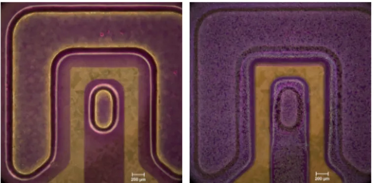
Two layers of photoresist materials are coated for the second copper etching step (steps (e) and (g)). This was found to be necessary because of the surface tension of the dip-coated resin (see Fig. 6): although it follows well the steep copper profile, the resin coat tends to be much thinner around the edges of the protruding features, so it doesn’t provide enough protection against the ferric chloride copper etchant. The dry-film photoresist is much thicker (75 µm), but it is too rigid to conform to the copper surface (Fig. 5(g)), so it cannot protect the lower copper surface properly (“tenting” effect). As a consequence, we decided to use both processes simultaneously: the liquid resin provides a high resolution, conformal coating, while the dry-film acts as an “umbrella” over the protruding features. This makes the overall process more complex, but was found to be necessary to achieve the high resolution described in section II.
Fig. 6. View of a protruding feature at steps (f) (left) and (h) (right). Due to surface tension, the resin coat is thinner on the edges of the feature and appears lighter (left picture), although the flat areas and the “cliffs” of the feature are well protected. A dry film photoresist is laminated on top (right picture) to provide additional protection.
(a) (b)
Fig. 7. Photograph of one of the “pockets” in the shadow mask used during the preparation of the dies, to perform selective Ti/Ag deposition. In this case, the pocket is 2.4 × 2.4 mm2.
B. Preparation of the SiC dies
As most power dies, the SiC JFET used here have an aluminium topside finish. Although this is well suited to wire-bond interconnects, it is not compatible with solder or silver sintering. As a workaround, some authors have used silver-loaded epoxy glue [33]. In this article, we apply an additional plating on top of the dies, using Physical Vapor Deposition (PVD). A custom shadow mask (Fig. 7) is manufactured (DBProducts) by bonding two stainless-steel stencils (250 µm and 50 µm thick): Large cutouts (same size as the die) are performed in the thick stencil, while the actual pattern to be plated (corresponding to the areas which will receive the metal plating) is cut in the thin stencil. Once bonded with the proper alignment, this creates a mask with locating pockets. The dies are simply placed manually in the pockets, and kept in place by a piece of polyimide tape. This technique is well suited to processing individual dies, with an alignment accuracy of ≈ 100 µm.
Once mounted in the shadow mask, the dies are placed in the PVD system (EVA300, electron beam heating), and receive 50 nm of Ti and 150 nm of Ag. No cleaning is performed on the dies either before or after plating. Once removed, the
polyimide adhesive was found to leave no residues on the backside of the dies.
C. Assembly
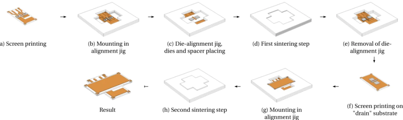
The assembly process is described in Fig. 8. It uses custom, laser-cut alumina parts as alignment jigs (the white parts in Fig. 8). The silver paste used here is made of micro-scale particles, and allow sintering under low pressure (Heræus LTS11702P2 or ASP295). A photograph of the parts to be assembled is given in Fig. 9.
(a) Silver paste is stencil-printed on one of the DBC sub-strates (using binoculars for proper stencil/substrate align-ment). A 50 µm-thick, laser cut, stainless steel stencil (DB Products) is used. The paste deposit is then dried for 5 min on a hotplate at 85 °C (Fig. 10).
(b) The substrate is placed in a ceramic jig.
(c) A second jig, with cutouts for the dies, is positioned. Two SiC dies are placed in the openings, gate and source facing downwards. A die Bonder (JFP PP One) is used at this stage to control the placement force (50 mN). (d) This stack is placed between the platens of a custom
heating press [34]. The sintering profile is as follows: a 30 min step at 85 °C, for drying, then a fast ramp (70 °C/min) to 240 °C. This temperature is maintained for 30 min for the actual sintering to take place, under a pressure of 2 MPa, and the assembly is left to cool down to room temperature.
(e) The small jig is removed before the second assembling step. At this stage, the gate and source of both dies are bonded to a DBC substrate. As this is the most critical stage of the process, a simple electrical test can be performed to ensure there are no short circuit or un-connected pads: a hand multimeter is used to check that gate and source have a capacitive behaviour (≈ 1-4 nF, depending of the die size)
(f) The second DBC substrate is stencil-printed and dried for 5 min at 85 °C. On both substrate, some more fresh paste is applied manually (with the tip of sharp tweezers) on the pad which contacts with the spacer, to ensure good contact (the spacer is only 350 µm-thick, while the dies are 380 µm-thick).
(g) The first DBC, the copper spacer and the second DBC are mounted in the alignment jig.
(h) The stack undergoes a second sintering step, with the same parameters as in step (d).
(i) The assembly is formed.
This process is made possible thanks to silver sintering: once sintered (at 240 °C), the paste forms a solid silver joint (which melts at 961 °C); therefore, it is possible to perform a second sintering step (Fig. 8(h)) without altering the result of the first (Fig. 8(d)). With soldering, this would have required two distinct soldering alloys to ensure different melting points (“staged assembly”, [24]).
Another special feature of the silver paste is the lack of liquid phase, as silver sintering is a solid-state phenomenon. This means that the displacement of bonding material only
(a) Screen printing (b) Mounting in alignment jig
(c) Die-alignment jig, dies and spacer placing
(d) First sintering step (e) Removal of die-alignment jig
(f) Screen printing on "drain" substrate (g) Mounting in
alignment jig (h) Second sintering step
Result
Fig. 8. Process flow for assembling the module: Alignment jigs are used to position the dies relatively to the first DBC tile (first sintering step), and to position both tiles relatively to each other (second sintering step).
Fig. 9. Parts set for the assembly: two substrates, two dies, and a small copper spacer. Left: version for 2.4×2.4 mm2dies, right: for 4×4 mm2 dies.
Fig. 10. Photograph of the DBC substrate (here for a 4×4 mm2die) with
stencil-printed silver paste.
occurs at the microscopic scale, during the densification of the silver powder into a solid. There is no macroscopic movement, as can be observed with solders due to the wetting phenomenon. The advantage is that this ensures the dies do not move during sintering (this could happen with soldering), so alignment is preserved. The downside is that there is no “tolerance” in the process: any misalignment, bridge, or bad contact between the die and the silver paste is preserved too. With solder, small issues tend to be self-corrected. A solution
Fig. 11. Effect of pre-drying of the paste: a small glass slide is placed over the paste deposit and the spreading is observed. Left: the paste was not dried before placing the glass slide. Right: the paste was dried for 5 mn at 85 °C.
is to take advantage of the viscous phase of the paste to provide some compliance during the positioning of the dies.
An example is visible in Fig. 11: here, a glass fragment is used in place of the die, to observe the spreading of the silver paste during the placement operation. If the die is placed directly on the fresh paste deposit, even a small force (50 mN) is enough to obtain a large spreading. If the paste is slightly dried (5 min at 85 °C for example), there is virtually no spreading but the paste retains some tackiness. The tackiness is required to prevent the die from moving when handling the assembly in the lab (to go from the die bonder to the sintering press).
Finally, after assembly, the module is encapsulated. Here, we use a layer of fluorinated parylene. This material was found to have an excellent long-term reliability at high temperature (more than 1000 h at 300 °C in [25], [28]). It has excellent dielectric properties (several MV/cm [25]). Furthermore, the chemical vapor phase deposition mechanism of this material ensures a conformal coating, with uniform deposition of a film of parylene, even on the most intricate geometries. This is well suited to the package described here, as small cavities (around the gate contact, for example) can be difficult to coat.
A photograph of the fully assembled package is given in Fig. 12.
Fig. 12. Photograph of the package once assembled. Each ceramic tile is 12.7×25.4 mm2.
0.00 0.05 0.10 0.15 0.20 0.25 0.30 0.35 0.40
Drain-Source Voltage [V]
0.0
0.2
0.4
0.6
0.8
1.0
1.2
Drain current [A]
-5.0 V -10.0 V -15.0 V -20.0 V -25.0 V -30.0 V
Fig. 13. Low level direct characteristic of a JFET which demonstrates proper modulation (the device is blocked for a VGS of -25 V).
IV. ANALYSIS OF THE PACKAGE
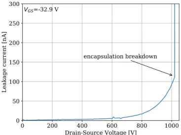
Results of a room-temperature static characterization of the power module are presented in Figs. 13 and 14. The direct characteristic is acquired using a Tektronix 371A curve tracer, using spring probes to contact with the power module (hence the limited measurement range for the current). The results show that the JFETs operate properly, with a -25 V threshold voltage (these devices are normally-on, i.e. are in the on-state in the absence of gate voltage).
In the blocked state, Fig. 14 shows that the leakage current remains low (< 10 nA) up to 600 V. Then, there is a gradual increase which is related to the JFET itself. At 1020 V, there is a dramatic increase in the leakage current which can be attributed to the breakdown of the encapsulation layer. Although breakdown occurred at a lower voltage than the rated voltage of the JFET (1200 V), it is must be noted that for this
0
200
400
600
800
1000
Drain-Source Voltage [V]
0
50
100
150
200
250
300
Leakage current [nA]
encapsulation breakdown
V
GS=-32.9 V
Fig. 14. Drain leakage current measured for a VGS of -32.8 V. At 1020 V,
a dielectric breakdown occurred, resulting in the non-reversible loss of the blocking capability.
sample, only 2 µm of parylene-D were used, for practical reasons. A thicker parylene layer (20 µm, as initially planned) should be sufficient to sustain 1200 V.
V. CONCLUSION
This article detailed a “sandwich” packaging structure suited to the operation of SiC devices. It only uses materials suited to high-temperature (> 300 °C). In particular, the assembly is performed using silver sintering for both sides of the dies.
A special care was given to the patterning of the DBC substrates, to form protruding features which mate with the SiC dies without interfering with their peripheral protection. The proposed copper etching technique has a sufficient reso-lution to allow the formation of small features (smaller than 0.4×0.6 mm2, with a spacing of 0.2 mm).
Future development will aim at reinforcing the mechani-cal strength of the package: at the moment, both substrates are assembled through the SiC dies (and the spacer). As a consequence, any external mechanical stress is transmitted to the dies, which makes the power module fragile. This could be prevented either by using a solid epoxy encapsulation (providing it is compatible with the operating temperature), such as in [14], or by forming separate protrusions on the DBC substrates to put them in direct contact (such as in [13]). The effect of the possible double-side cooling on the thermal resistance of the package should also be assessed.
ACKNOWLEDGMENT
This work was supported through the grants EPAHT (French National Fundation for Aeronautic and Space Research -FNRAE) and THOR (EURIPIDES-CATRENE). The authors would like to acknowledge the use of the NanoLyon platform.
REFERENCES
[1] D. Bergogne, D. Tournier, R. Mousa, M. Shafiee Koor, D. Planson, H. Morel, and B. Allard, “SiC JFET for high temperature power switches,” in Proceedings of the Conference on Integrated Power Sys-tems (CIPS). N¨uremberg, Germany: VDE Verlag, Mar. 2008, pp. 253– 256.
[2] T. Funaki, J. C. Balda, J. Junghans, A. S. Kashyap, H. A. Mantooth, F. Barlow, T. Kimoto, and H. Takashi, “Power Conversion With SiC Devices at Extremely High Ambient Temperatures,” IEEE Transactions on Power Electronics, vol. 22, no. 4, pp. 1321–1329, Jul. 2007. [3] C. Buttay, D. Planson, B. Allard, D. Bergogne, P. Bevilacqua, C. Joubert,
M. Lazar, C. Martin, H. Morel, D. Tournier, and C. Raynaud, “State of the art of high temperature power electronics,” Materials Science and Engineering: B, vol. 176, no. 4, pp. 283–288, 2011, microtechnology and Thermal Problems in Electronics.
[4] J. Mill´an, P. Godignon, X. Perpi˜n`a, A. P´erez-Tom´as, and J. Rebollo, “A Survey of Wide Bandgap Power Semiconductor Devices,” IEEE transactions on Power Electronics, vol. 29, no. 5, pp. 2155–2163, May 2014.
[5] K. Sheng, “Maximum Junction Temperatures of SiC Power Devices,” IEEE Transactions on Electron Devices, vol. 56, no. 2, pp. 337–342, Feb. 2009.
[6] C. Buttay, C. Raynaud, H. Morel, G. Civrac, M.-L. Locatelli, and F. Morel, “Thermal Stability of Silicon Carbide Power Diodes,” IEEE Transactions on Electron Devices, vol. 59, no. 3, pp. 761–769, 2012. [7] C. Buttay, R. Ouaida, H. Morel, D. Bergogne, C. Raynaud, and F. Morel,
“Thermal Stability of Silicon Carbide Power JFETs,” IEEE transactions on Electron Devices, vol. 60, no. 12, pp. 4191–4198, Dec. 2013. [8] L. M´enager, C. Martin, B. Allard, and V. Bley, “Industrial and lab-scale
power module technologies : A review,” in Proceedings of the 32nd Annual Conference of the IEEE Industrial Electronics Society (IECON), IEEE, Ed., Paris, France, Nov. 2006.
[9] A. Alderman, L. Burgyan, B. Narveson, and E. Parker, “3-D Embedded Packaging Technology,” IEEE Power Electronics Magazine, pp. 30–39, dec 2015.
[10] J. Schulz-Harder, “Review on Highly Integrated Solutions for Power Electronic Devices,” in Proceedings of the Conference on Integrated Power electronics Systems (CIPS), N¨uremberg, Mar. 2008, p. 7 p. [11] P. Solomalala, J. Saiz, A. Lafosse, M. Mermet-Guyennet, A. Castellazzi,
X. Chauffieur, and J.-P. Fredin, “Multi-domain simulation platform for virtual prototyping of integrated power systems.” in Power Electronics and Applications, 2007 European Conference on, Sep. 2007, pp. 1–10. [12] J. Li, A. Castellazzi, A. Solomon, and C. M. Johnson, “Reliable Integration of Double-Sided Cooled Stacked Power Switches based on 70 µm Thin IGBTs and Diodes,” in Proceedings of the 7thConference on Integrated Power Systems, VDE, Ed., Nuremberg, Mar. 2012, pp. 131–136.
[13] C. Buttay, J. Rashid, C. Johnson, F. Udrea, G. Amaratunga, P. Ireland, and R. Malhan, “Compact Inverter Designed for High-Temperature Operation,” in Proc. IEEE Power Electronics Specialists Conference PESC 2007, 2007, pp. 2241–2247.
[14] A. Grassmann, O. Geitner, W. Hable, C. Neugirg, A. Schwarz, F. Winter, and I. Yoo, “Double Sided Cooled Module concept for High Power Density in HEV Applications,” in Proceedings of the International Exhibition and Conference for Power Electronics, Intelligent Motion, Renewable Energy and Energy Management (PCIM). N¨uremberg, Germany: VDE Verlag, May 2015, pp. 442–448.
[15] D. Woo, H. H. Yuan, J. Li, H. S. Ling, L. J. Bum, Z. Songbai, Z. Hengyun, S. Selvaraj, S. Velez, and R. Singh, “High power SiC inverter module packaging solutions for junction temperature over 220 °C,” in Electronics Packaging Technology Conference (EPTC), 2014 IEEE 16th, Dec 2014, pp. 31–35.
[16] M. Knoerr, S. Kraft, and A. Schletz, “Reliability Assessment of Sintered Nano-Silver Die Attachment for Power Semiconductors,” in Proceedings of the 12th Electronics Packaging Technology Conference (EPTC). Singapore: IEEE, Dec. 2010, pp. 56–61.
[17] V. Manikam and K. Y. Cheong, “Die Attach Materials for High Temperature Applications: A Review,” Components, Packaging and Manufacturing Technology, IEEE Transactions on, vol. 1, no. 4, pp. 457–478, Apr. 2011.
[18] R. Khazaka, L. Mendizabal, D. Henry, and R. Hanna, “Survey of High-Temperature Reliability of Power Electronics Packaging Components,”
Power Electronics, IEEE Transactions on, vol. 30, no. 5, pp. 2456–2464, May 2015.
[19] G.-Q. Lu, J. Calata, G. Lei, and X. Chen, “Low-temperature and pres-sureless sintering technology for high-performance and high-temperature interconnection of semiconductor devices,” in Thermal, Mechanical and Multi-Physics Simulation Experiments in Microelectronics and Micro-Systems, 2007. EuroSime 2007. International Conference on. IEEE, 2007, pp. 1–5.
[20] T. G. Lei, J. N. Calata, G.-Q. Lu, X. Chen, and S. Luo, “Low-Temperature Sintering of Nanoscale Silver Paste for Attaching Large-Area (> 100mm2) Chips,” IEEE Transaction on Components and Packaging Technology, vol. 33, no. 1, pp. 98–104, Mar. 2010. [21] C. Mertens, J. Rudzki, and R. Sittig, “Top-Side Chip Contacts with Low
Temperature Joining Technique (LTJT),” in Proceedings of the 2004 IEEE 35thannual power electronics specialists conference (PESC 04). Aachen: IEEE, Jun. 2004, pp. 4178–4182.
[22] T. Stockmeier, P. Beckedahl, C. Gobl, and T. Malzer, “SKiN: Double side sintering technology for new packages,” in Power Semiconductor Devices and ICs (ISPSD), 2011 IEEE 23rdInternational Symposium on,
May 2011, pp. 324–327.
[23] F. Kato, F. Lang, S. Rejeki, H. Nakagawa, H. Yamaguchi, and H. Sato, “Precise Chip Joint Method with Sub-micron Au Particle for High-density SiC Power Module Operating at High Temperature,” in Proceed-ings of the High Temperature Electronics Network Conference (HiTEN 2013), 2013.
[24] D. Berry, L. Jiang, Y. Mei, S. Luo, K. Ngo, and G. Q. Lu, “Packaging of high-temperature planar power modules interconnected by low-temperature sintering of nanosilver paste,” in Electronics Packaging (ICEP), 2014 International Conference on, April 2014, pp. 549–554. [25] S. Diaham, M.L. Locatelli, and Z. ValdezNava, Silicon Carbide
-Materials, Processing and Applications in Electronic Devices. Intech, Oct. 2011, ch. 17 - Dielectrics for High Temperature SiC Device Insulation: Review of New Polymeric and Ceramic Materials, pp. 409– 430.
[26] Y. Yao, Z. Chen, G.-Q. Lu, D. Boroyevich, and K. D. T. Ngo, “Charac-terization of Encapsulants for High-Voltage, High-Temperature Power Electronic Packaging,” in Proceedings of the Electronic Components and Technology Conference 2010. Las Vegas, Nevada: IEEE, Jun. 2010, p. 7.
[27] M. L. Locatelli, S. Diaham, Z. Valdez-Nava, M. Bechara, and R. Khaz-aka, “Suitable Characterization Methods and Insulating Materials for Devices Operating above 200◦C,” Advanced Materials Research, vol. 324, pp. 229–232, Aug. 2011.
[28] R. Riva, C. Buttay, B. Allard, and P. Bevilacqua, “Migration issues in sintered-silver die attaches operating at high temperature,” Microelec-tronics Reliability, vol. 53, pp. 1592–1506, 2013.
[29] Y. Mei, D. Ibitayo, X. Chen, S. Luo, and G.-Q. Lu, “Migration of Sintered Nanosilver Die-attach Material on Alumina Substrate at High Temperatures,” in Proceedings of the IMAPS International Conference and Exhibition on on High Temperature Electronics (HiTEC 2010). albuquerque, NM: IMAPS, May 2010, pp. 26–31.
[30] R. Riva, C. Buttay, M.-L. Locatelli, V. Bley, and B. Allard, “Design and Manufacturing of a Double-Side Cooled, SiC based, High Temperature Inverter Leg,” in Proceedings of the High Temperature Electronics Conference and Exhibition, HiTEC 2014. Albuquerque, NM: IMAPS, May 2014.
[31] Curamik, “curamik Ceramic Substrates DBC technology – Design Rules,” Rogers Curamik, Tech. Rep., dec 2014.
[32] S. Hasco¨et, C. Buttay, D. Planson, R. Chiriac, and A. Masson, “Pres-sureless Silver Sintering Die-Attach for SiC Power Devices,” Materials Science Forum, vol. 740, pp. 851–854, 2012.
[33] M. Barri`ere, S. Azzopardi, R. Roder, I. Favre, E. Woirgard, S. Bontemps, and F. Le Henaff, “Silver Sintered Double-Sided Cooling Power Package Process for Controlled Si Power Semiconductor Devices With Alu-minum Top-Metallization,” in Proceedings of the International Work-shop on Integrated Power Packaging, 2015.
[34] C. Buttay, A. Masson, J. Li, M. Johnson, M. Lazar, C. Raynaud, and H. Morel, “Die Attach of Power Devices Using Silver Sintering -Bonding Process Optimisation and Characterization,” in Proceedings of the High Temperature Electronics Network Conference (HiTEN 2011). Oxford, UK: IMAPS, Jul. 2011, pp. 84–90.