HAL Id: lirmm-01548938
https://hal-lirmm.ccsd.cnrs.fr/lirmm-01548938
Submitted on 28 Jun 2017
HAL is a multi-disciplinary open access
archive for the deposit and dissemination of
sci-entific research documents, whether they are
pub-lished or not. The documents may come from
teaching and research institutions in France or
abroad, or from public or private research centers.
L’archive ouverte pluridisciplinaire HAL, est
destinée au dépôt et à la diffusion de documents
scientifiques de niveau recherche, publiés ou non,
émanant des établissements d’enseignement et de
recherche français ou étrangers, des laboratoires
publics ou privés.
A novel SRAM -STT-MRAM hybrid cache
implementation improving cache performance
Odilia Coi, Guillaume Patrigeon, Sophiane Senni, Lionel Torres, Pascal Benoit
To cite this version:
Odilia Coi, Guillaume Patrigeon, Sophiane Senni, Lionel Torres, Pascal Benoit. A novel SRAM
-STT-MRAM hybrid cache implementation improving cache performance. NANOARCH: Nanoscale
Architectures, Jul 2017, Newport, United States. pp.39-44, �10.1109/NANOARCH.2017.8053704�.
�lirmm-01548938�
A novel SRAM - STT-MRAM hybrid cache
implementation improving cache performance
Odilia Coi, Guillaume Patrigeon, Sophiane Senni, Lionel Torres, Pascal Benoit
LIRMM-UMR CNRS 5506 University of Montpellier
Montpellier, France [email protected]
Abstract—Memories are currently a real bottleneck to design high speed and energy-efficient systems-on-chip. A significant in-crease of the performance gap between processors and memories is observed. On the other hand, an important proportion of total power is spent on memory systems due to the increasing trend of embedding volatile memory into systems-on-chip. For these reasons, STT-MRAM (Spin-Transfer Torque Magnetic Random Access Memory) is seen as a promising alternative solution to traditional SRAM (Static Random Access Memory) thanks to its negligible leakage current, high density, and non-volatility. Nevertheless, the strategy of the same footprint replacement is constrained by the high write energy/latency of STT-MRAM. This paper performs a fine-grained evaluation of the cache organization to propose a hybrid cache memory architecture including both SRAM and STT-MRAM technologies.
I. INTRODUCTION ANDRELATEDWORKS
Several studies, for instance in [1], [2], [3], explored the combination of STT-MRAM and SRAM to propose fast and low-power cache memories. Novel management techniques have been proposed to mitigate the high write energy/latency of STT-MRAM based cache such as in [4], [5], [6]. Other works explored the performance improvement of STT-MRAM by reducing the retention time [7], [8].
This paper evaluates a novel hybrid cache architecture by building the tag arrays and the data arrays with two different memory technologies (SRAM and STT-MRAM). A fined-grained exploration at circuit level thanks to NVSim [9] and at architecture level thanks to gem5 [10] and McPAT [11] was carried out to achieve the best tradeoff regarding the three metrics: latency, power, area. Compared to other technologies such as Phase-Change Memory (PCM) and Resistive memory (RRAM), STT-MRAM is clearly the most competitive in terms of access latency according to the state of the art [12]. Moreover, STT-MRAM demonstrates a very high endurance (about 1015 cycles [13]) which is essential for frequently accessed memories such as caches. Regarding the circuit implementation, this work proposes a hybrid memory by exploiting the inherent architecture of cache with separated tag arrays and data arrays. Hence, the design of such a hybrid cache is more convenient for manufacturing than previous solutions which divide tag arrays and data arrays into different regions to consider different memory technologies [2], [3].
The rest of the paper is organized as follows: Section II is dedicated to the circuit-level analysis, Section III presents the
hybrid cache and its performances, a system-level analysis is presented in Section IV and Section V concludes this paper.
II. CIRCUIT-LEVEL ANALYSIS
This section focuses on the performance analysis of the tag array and the data array of a cache memory considering differ-ent associativities and differdiffer-ent cache sizes, for a technology node of 32 nm.
The cache line size is fixed at 64 Bytes and a room temperature is considered. This study was performed thanks to NVSim, a performance, energy, and area estimator for Non-Volatile Memories (NVM) which uses an empirical modeling methodology based on the well-known CACTI [14]. Based on circuit-level data of single bit cell and the desired memory architecture information such as capacity, data width, and type of memory (e.g. Cache, RAM, CAM), NVSim estimates the access time, the access energy, and the total area of a complete NVM chip. This tool also includes optimization settings (e.g. buffer design optimization) and various design constraints to facilitate the design space exploration before the fabrication of the actual NVM chip.
A. Tag array
Tag array is a small, every clock cycle accessed memory containing the upper part of the memory address. This sug-gest that low read latency and low power consumption are mandatory requirement in an efficient cache organization.
1) 32 kB cache: The memory organization for a small cache size (here 32 kB) was first explored.
TABLE I
ASSOCIATIVITY IMPACT ON CACHE ORGANIZATION
Associativity 2 4 8 16 Bank 1x1 1x1 1x1 1x1
Mat 1x1 1x1 2x1 1x1 Sub-array 256x72 128x148 64x152 32x164
The associativity impact on the cache sub-array organization is reported in Table I. When doubling the associativity degree, the tag array size increases by around 5%. The same result is predictable using the following relation:
(a)
(b)
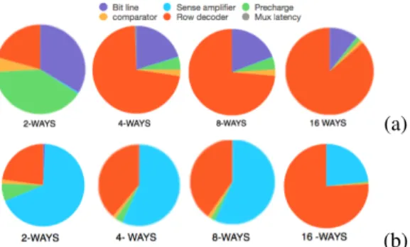
Fig. 1. Tag sub-array read latency in a 32 kB cache (a) SRAM tag array (b) STT-MRAM tag array
Fig. 2. Tag array read latency (1 MB cache)
Where:
• TagSize is the tag field of the memory address, which increases by 1 bit when the associativity is doubled.
• NoSets is the number of sets (i.e. the number of cache line per tag array).
• NoWays is the number of ways (i.e. the number of tag
arrays).
As the number of rows per columns changes, the weight of the peripheral circuits on the overall performance changes too. Since the tag array is read for each cache access, the latency of this operation is a critical parameter.
• Tag array in SRAM
• Tag array in STT-MRAM
Fig. 1 shows that for a small size memory, the latency is mainly due to the peripherals circuits.
Because of its small cell size, STT-MRAM based tag array shows a negligible bitline latency. However, it remains slower than a SRAM-based tag array because of the latency of the peripheral circuits, especially the row decoder and the sense amplifiers.
Because STT-MRAM requires large CMOS transistors for the peripheral circuits, this technology is not suitable to build tag array of cache memories according to this analysis.
2) 1 MB cache: A global performance comparison between SRAM and STT-MRAM tag is carried out for a 1MB cache in Figures 2, 3, 4, 5, 6 and 7.
Fig. 3. Tag array write latency (1 MB cache)
Fig. 4. Tag array read dynamic energy (1 MB cache)
Results concerning read and write dynamic power and latency show a clear superiority of SRAM over STT-RAM. Write dynamic energy and write latency are actually the two main drawbacks linked with the physical structure of STT-RAM. They penalize this technology in small cache size.
It is interesting to notice that latency results (Fig. 3 and Fig. 2) of 8-way set associativity for STT-MRAM cache are the highest. This is due to non linearity issues in 8-way set and the impossibility to set some constraints in the sub-array organization in NVSim (such as force the number of banks, mats and sub-arrays as well as number of bit-lines connected to the same multiplexer).
As expected, the main strength of STT-MRAM cells is in leakage consumption as shown in Table II (only the peripheral circuits and access transistors contribute to the static power consumption).
TABLE II
ASSOCIATIVITY IMPACT ON LEAKAGE CONSUMPTION
Associativity 2 4 8 16 SRAM tag [mW] 96.9 100.4 102.3 105.2 STT-MRAM tag [mW] 1.1 1.5 1.5 2.2
Regarding the area (Fig. 6), STT-MRAM tag array over-comes SRAM tag array for every associativity degree, because the bit cells area contribution become more important than the peripheral circuits area contribution for large arrays.
Fig. 5. Tag array write dynamic energy (1 MB cache)
Fig. 6. Tag array area (1 MB cache)
B. Data array
Data array is the part of the cache in which data are stored. As for the tag array analysis, this section explores the impact of the associativity on the data array performance.
• Data array in SRAM:
The overall performance of SRAM-based data array does not change significantly when varying the associativity. Up to 0.5% of variation is observed for the access latency. The energy consumption remains roughly constant.
• Data array in STT-MRAM:
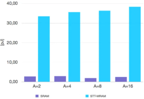
As for SRAM, STT-MRAM based data array keeps the same overall performance by changing the associativity. However, the write dynamic energy decreases linearly with the increase of the associativity, as shown in Ta-ble III.
TABLE III
SET/RESET DYNAMIC ENERGY AND ASSOCIATIVITY IMPACT IN A1 MB
DATA ARRAY
Associativity 2 4 8 16 MuxSenseAmpl 8 4 2 1 Set/reset dynamic energy [nJ] 69.5 34.8 17.4 8.7
In Table III, MuxSenseAmpl represents the number of bit-lines connected to each sense amplifier, and Set/reset dynamic energy represent the write dynamic energy per sub-array.
If multiples bit-lines are connected to one sense amplifier, all these bit-lines have to be biased when a single write occurs,
Fig. 7. STT-MRAM data array size and their advantages in NVSim metrics (worst case)
that is why the write dynamic energy is inverse correlated to the associativity.
A performance comparison between the two memory tech-nologies considering different cache sizes was explored. Re-sults are summarized in Fig. 7.
To summarize:
• STT-MRAM arrays are better than SRAM ones concern-ing leakage for every data array size.
• STT-MRAM arrays are denser, and so smaller than SRAM arrays.
• For small memory sizes, the area is dominated by periph-eral circuits, so STT-MRAM is larger than SRAM.
• Still for small memory sizes, the latency is dominated by
peripheral circuits, so STT-MRAM is slower than SRAM.
• When the size is large enough to make the peripheral
circuits latency and area negligible compared to the cell array, SRAM memory is slower for read operations and larger than STT-MRAM.
III. HYBRID CACHE
Using the following considerations:
• For small cache size, tag array area and timing perfor-mances are dominated by peripheral circuits, and STT-RAM is better than SSTT-RAM only for leakage consumption.
• For large data array, STT-MRAM is better than SRAM
for area, latency and leakage.
• Increasing associativity while keeping constant the
num-ber of columns and rows, lead to decrease the write dynamic energy.
We propose a novel hybrid cache organized as follows:
• Tag array in SRAM
• Data array in STT-RAM
A. Experimental setup
Based on the observations of Section II, size and associa-tivity are chosen for their promising results in leakage, area, read latency, read dynamic energy and write dynamic energy: 1 MB, 16-way set associative cache.
Three transistor types were considered:
• High Performance (HP)
• Low Operating Power (LOP)
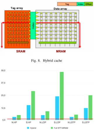
Fig. 8. Hybrid cache
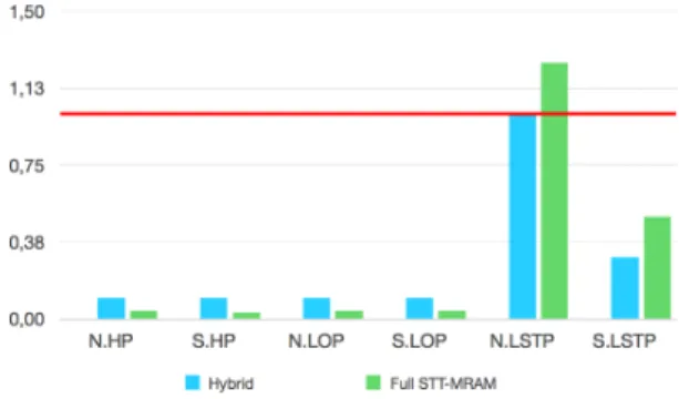
Fig. 9. 1 MB 16-way write dynamic energy (relative to classic SRAM)
Different access modes were also explored:
• Normal access: tag and data array are accessed in the same clock cycle.
• Sequential access: tag array is accessed in the first clock
cycle, then only if an hit occurs the corresponding data array is accessed during the following clock cycle. All results, labeled with HP, LOP or LSTP, preceded by N. (Normal) or S. (Sequential), have been normalized to the SRAM baseline performances.
B. Performances
For each scenario, the write dynamic energy of the hybrid cache is midway between full SRAM and full STT-MRAM write energies (Fig. 9). As expected, a 1 MB cache memory with hybrid banks has worst performances than a full SRAM in write dynamic energy, due to the impact of the STT-MRAM data array. But this is better than for full STT-MRAM, thank to the SRAM tag array.
This improvement will also limit the power dissipated in write operations, caused by the required current to flip the spin state.
During a cache block replacement, NVSim writes tag and data in parallel, and so the latency is defined by the worst latency between tag write and data write (here, the data write). This is why the write latency in hybrid banks is always the same as the latency in full STT-MRAM ones (Fig. 10).
Fig. 11 shows that in most of the scenario, the hybrid cache requires lower read energy than SRAM.
Fig. 10. 1 MB 16-way write latency (relative to classic SRAM)
Fig. 11. 1 MB 16-way cache read dynamic energy (relative to classic SRAM)
For the LOP mode with normal access, hybrid bank per-formances exceeded baseline about 35%. In the LOP mode, electrical SRAM CMOS parameters (Vdd, Vth, Cox...) are modified in order to have a strong cache dynamic energy reduction.
However, the hybrid cache still requires lower energy than full STT-MRAM for read operations.
As expected, the hybrid bank has the best read latency in sequential access mode: in tag array SRAM is faster than STT-MRAM, and in large data array STT-MRAM is the fastest. In the normal access mode, the hybrid bank has the same performances as STT-MRAM banks.
For now, the hybrid cache is at least equal or better than the full STT-MRAM cache.
Fig. 13 shows that the leakage current is greatly decreased when using a STT-MRAM data array; the remaining leakage is due to the peripheral circuits. Even if using a SRAM tag affects this leakage current, the global leakage is still very lower than the leakage of a classic SRAM cache.
Like for the leakage current, Fig. 14 shows that a STT-MRAM data array is better in term of area than a SRAM one. For large cache sizes, using a SRAM tag rather than a STT-MRAM tag does not have a great impact on the area.
To summarize:
• Read latency and dynamic energy: hybrid cache are better than SRAM and full STT-MRAM caches.
• Write latency: hybrid cache, like full STT-MRAM cache, are a little slower than SRAM cache.
Fig. 12. 1 MB 16-way cache read latency (relative to classic SRAM)
Fig. 13. 1 MB 16-way cache leakage (relative to classic SRAM)
• Area and leakage: hybrid cache is not as good as full STT-MRAM cache, but still far better than SRAM cache.
• Write dynamic energy: hybrid cache are halfway between SRAM and full STT-MRAM caches.
IV. SYSTEM-LEVEL ANALYSIS
In order to go further and analyze the potential gains of a hybrid cache over full SRAM and full STT-MRAM in a realistic scenario, some applications have been simulated using these architectures with the gem5 simulator [10], a processor architecture simulator, and McPAT [11], an integrated power, area, and timing modeling framework. Details of the simulated architectures are shown in Table IV. Different workloads of the Parsec 3.0 suite have been simulated, and results are summarized in Fig. 15.
TABLE IV SIMULATED ARCHITECTURE
Core ARMv7 ISA 1 GHz (out of order) L1 data Private SRAM 32 kB L1 Instruction Private SRAM 32 kB
L2 Shared SRAM / STT-MRAM / Hybrid 1MB Main memory DDR3 512 MB
The timing performance of STT-MRAM over SRAM is really dependent of the application. But, the hybrid cache is always better than a full STT-MRAM caches, as expected.
Fig. 14. 1 MB 16-way cache area (relative to classic SRAM)
Fig. 15. Normalized run time, 4 cores at 1 GHz
As expected too, the low-leakage of the STT-MRAM has a clear impact on the L2 cache energy consumption, as shown in Fig. 16.
Looking at the global energy consumption in Fig. 17, the cores represent a large part of the energy consumption, and the more cores there are the larger is that part. Still, the L2 cache is the second largest part. It represent early 33% of the global energy consumption in the mono-core architecture for this application. There is clearly a huge advantage to use STT-MRAM in caches in order to reduce the microprocessor consumption.
Finally, there is no relevant differences in global energy con-sumption using full STT-MRAM or hybrid cache. The gains are dependent of the running application and the architecture, so the main difference is in timing.
V. CONCLUSION AND PERSPECTIVES
A fine-grained tag array and data array study was exposed in this paper and a novel hybrid cache organization was proposed. Simulations results show that the hybrid cache is a balanced solution which uses both SRAM and STT-MRAM advantages: reducing the energy consumption while maintaining a low-latency response.
Architecture-level simulations demonstrate that the hybrid cache is indeed better in consumption than a classic SRAM cache, and so we can reduce the global consumption of an architecture using STT-MRAM technology. Also, the hybrid cache is faster than a full STT-MRAM cache, and their impact
Fig. 16. Normalized L2 cache energy, 4 cores at 1 GHz
on the global energy consumption are nearly the same for the considered applications.
To go further and enhanced this analysis, a more detailed approach should be done by using parameters of real im-plementations, in order to obtain a finer comparison and estimation of the gains of the hybrid cache over a full STT-MRAM cache.
ACKNOWLEDGMENT
This work has received funding from the European Union’s Horizon 2020 research and innovation program under grant agreement No 687973 (GREAT project) and the French Na-tional Research Agency under grant ANR-15-CE24-0033-01 (MASTA project).
REFERENCES
[1] W. Xu, H. Sun, X. Wang. Y. Chen, T. Zhang, “Design of Last-Level On-Chip Cache Using Spin-Torque Transfer RAM (STT RAM)”, Very Large Scale Integrated Systems, IEEE Transactions on vol. 19, no. 3, pp. 483-493, 2011.
[2] X. Wu et al., “Hybrid cache architecture with disparate memory tech-nologies”, ACM SIGARCH Comput. Architect. News, vol. 37, no. 3, pp. 3445, 2009.
[3] X. Wu, J. Li, L. Zhang, E. Speight, and Y. Xie, “Power and performance of read-write aware hybrid caches with non-volatile memories”, in IEEE Design, Automat. Test Eur. Conf. Exhibit., 2009, pp. 737742.
[4] P. Zhou, B. Zhao, J. Yang, and Y. Zhang, “Energy reduction for STT-RAM using early write termination”, Computer-Aided Design-Digest of Technical Papers, 2009. IC- CAD 2009. IEEE/ACM International Conference on. IEEE, pp. 264-268, 2009.
[5] K. -W. Kwon, S. H. Choday, Y. Kim, and K. Roy, “Aware (asym-metric write architecture with redundant blocks): A high write speed STT-MRAM cache architecture”, Very Large Scale Integration (VLSI) Systems, IEEE Transactions on, vol. 22, no. 4, pp. 712-720, 2014. [6] J. Wang, X. Dong, and Y. Xie, “OAP: An obstruction-aware cache
management policy for STT-RAM last-level caches”, in Proc. Conf. Design, Automat. Test Eur. Consort., 2013, pp. 847852.
[7] W. -K. Cheng et al., “Architecture and data migration methodology for L1 cache design with hybrid SRAM and volatile STT-RAM configuration”, Microprocessors and Microsystems 2015.
[8] A. Jog, A. K. Mishra, C. Xu, Y. Xie, V. Narayanan, R. Iyer, and C. R. Das, “Cache revive: Architecting volatile STT-RAM caches for enhanced performance in CMPs”, in Proceedings of the 49th Annual Design Automation Conference. ACM, pp. 243-252, 2012.
[9] X. Dong, C. Xu, Y. Xie, and N. P. Jouppi, “Nvsim: A circuit-level performance, energy, and area model for emerging nonvolatile memory”, Computer-Aided Design of Integrated Circuits and Systems, IEEE Trans-actions on, vol. 31, no. 7, pp. 994-1007, 2012.
(a)
(b)
(c)
Fig. 17. Energy consumption repartition for Canneal benchmark, (a) 1 core (b) 2 cores (c) 4 cores at 1 GHz
[10] N. Binkert, B. Beckmann, G. Black, S. K. Reinhardt, A. Saidi, A. Basu, J. Hestness, D. R. Hower, T. Krishna, S. Sardashti et al., “The gem5 simulator”, ACM SIGARCH Computer Architecture News, vol. 39, no. 2, pp. 17, 2011.
[11] S. Li, J. H. Ahn, R. D. Strong, J. B. Brockman, D. M. Tullsen, and N. P. Jouppi, “Mcpat: an integrated power, area, and timing modeling frame-work for multicore and manycore architectures”, in Proceedings of the 42nd Annual IEEE/ACM International Symposium on Microarchitecture. ACM, 2009, pp. 469480.
[12] Jagan Singh Meena, Simon Min Sze, Umesh Chand, and Tseung-Yuen Tseng, “Overview of emerging nonvolatile memory technologies”, in Nanoscale Res. Lett. 9, 1 (2014), 133.
[13] Y. Huai, J. Zhang, Y. Zhou, X. Wang, E. Abedifard, Z. Wang, X. Hao, D. Jung, K. Satoh, H. Gan et al., “PMTJ driven STTMRAMwith 300mm process”, in IEEE Magnetics Conference (INTERMAG) 2015, IEEE, 11. [14] N. Muralimanohar, R. Balasubramonian, and N. P. Jouppi, “Cacti 6.0:

![Montage expérimental et modèle de Hecht pour la caractérisation de la collection de charge [beta] de détecteurs au silicium](data:image/gif;base64,R0lGODlhAQABAIAAAP///wAAACH5BAEAAAAALAAAAAABAAEAAAICRAEAOw==)