Cathodoluminescence Mapping of Cherenkov-Radiation Generated Bloch-Modes
in Planar Photonic Crystals by Fast Electrons
D.T.L. Alexander,* N. Le Thomas,** S.D. Schneider,*** R. Houdré,** M. Cantoni,* and C. Hébert***
* Centre Interdisciplinaire de Microscopie Électronique (CIME), École Polytechnique Fédérale de Lausanne (EPFL), Lausanne, CH-1015, Switzerland
** Laboratoire d'Optoélectronique Quantique (LOEQ), École Polytechnique Fédérale de Lausanne (EPFL), Lausanne, CH-1015, Switzerland
*** Laboratoire de Spectrométrie et Microscopie Electronique (LSME), École Polytechnique Fédérale de Lausanne (EPFL), Lausanne, CH-1015, Switzerland
We report on the use of electron microscopy to study the optical properties of photonic devices, such as planar photonic crystal (PhC) waveguides and cavities. By using the Cherenkov effect, the optical mode profiles of photonic structures can be investigated with cathodoluminescence (CL) and electron energy-loss spectroscopy (EELS) techniques. Spatial resolutions of a few nm are achieved, whereas diffraction limits them to a few µm for conventional optical characterization tools.
The photonic structures consist of triangular photonic lattices of holes etched in 220 nm thick Si membranes. Tiles, line defects and three-missing-holes cavities have been designed to operate in the near infrared region (lattice constant a = 460 nm and a filling factor f = 35%). We will mainly focus on work using cathodoluminescence. A CL-detection equipped JEOL 2200FS scanning TEM (STEM) [1] is used for two main reasons. Firstly, because the small (≤ 2 nm) focused electron probe, combined with the thin 220 nm thickness of the Si membrane, produce an interaction volume with excellent spatial resolution. Secondly, by using a 200 keV beam, the sample is probed with electrons that are fast enough to stimulate emission of Cherenkov radiation; this Cherenkov radiation is coupled to the Bloch modes of the photonic crystal structures. Bloch modes, whose angular spectrum falls within the light cone, as for instance in the case of a cavity Bloch mode, can be backward-detected using CL. In the current detection scheme, i.e. the electron beam perpendicular to the Si membrane, only TM polarized modes are excited.
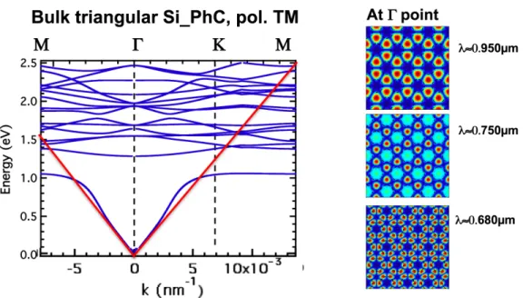
Fig. 1 shows calculations of 2D Bloch mode maps that might be expected for PhC tile structures; calculations are based on a guided mode expansion technique. While the simulations are still preliminary, and do not account for all possible guided modes in the planar waveguide, it is clear that modulations of CL signals are expected, and further that such modulations depend on wavelength. The STEM-based CL system has been used to acquire CL spectrum images. Fig. 2 shows maps determined for different wavelength ranges from a data cube acquired over a 75 x 75 pixel array with a CCD camera recording the spectrum from 500–775 nm wavelength. The CL intensities clearly show strong modulations depending on position and wavelength, as expected from the preliminary modeling. Also, unexpected symmetries are observed, pointing to this technique’s ability to analyse the physical properties of photonic crystals with a spatial resolution of nm.
Current research is exploring these possibilities for measurement of photonic properties further. For instance, in addition to continuing CL measurements and improving their simulations, efforts are underway to correlate results with those from extremely (sub 1 eV) low-loss EELS to measure
828
doi:10.1017/S1431927610060630 © Microscopy Society of America 2010Microsc. Microanal. 16 (Suppl 2), 2010
https://doi.org/10.1017/S1431927610060630
radiation from TE confined modes, similar to work by [2]. Concepts for creating waveguides with a well-defined TM guided mode for STEM investigations are also being considered.
References
[1] Mouti et al., “Cathodoluminescence in a (S)TEM – exploring possibilities and limits” submitted to MSA 2010, Portland.
[2] Yurtsever et al., PRL, 100, (2008) 217402.
[3] CCMX is acknowledged for the CL funding, and SNF project 200021-120308, the MP0702 COST action and the Swiss NCCR-Quantum Photonics for photonic research funding. Jean-Daniel Ganière of the LOEQ, EPFL is thanked for assisting the collaboration.
FIG. 1. Simulated dispersion curves and 2D maps of TM Bloch modes in Si membrane triangular photonic crystal. Red lines: Light lines.
FIG. 2. STEM image (left) of PhC tile structure with region chosen for CL spectrum image (SI) marked by the square. SI data was acquired for 75 x 75 pixels with a 500–775 nm wavelength range with an acquire time of 15 s per pixel for a total map time of 23 h. On the right are three slices of the SI CL data cube, after filtering to remove cosmic X-ray spikes and binning the wavelength axis by 40 times. Strong CL wavelength-dependent spatial modulations are seen. Horizontal lines probably result from detector gain variations resulting from temporary CCD temperature fluctuations.
λ = 499–507 nm λ = 614–622 nm λ = 655–663 nm
Microsc. Microanal. 16 (Suppl 2), 2010 829
https://doi.org/10.1017/S1431927610060630