HAL Id: tel-01097095
https://tel.archives-ouvertes.fr/tel-01097095
Submitted on 18 Dec 2014HAL is a multi-disciplinary open access
archive for the deposit and dissemination of sci-entific research documents, whether they are pub-lished or not. The documents may come from teaching and research institutions in France or abroad, or from public or private research centers.
L’archive ouverte pluridisciplinaire HAL, est destinée au dépôt et à la diffusion de documents scientifiques de niveau recherche, publiés ou non, émanant des établissements d’enseignement et de recherche français ou étrangers, des laboratoires publics ou privés.
light emitting devices with high indium concentrated
(In,Ga)N quantum wells
Sakhawat Hussain
To cite this version:
Sakhawat Hussain. Structural and optical characterization of green-yellow light emitting devices with high indium concentrated (In,Ga)N quantum wells. Physics [physics]. Univeristé Nice Sophia Antipolis, 2014. English. �tel-01097095�
UNIVERSITE DE NICE-SOPHIA ANTIPOLIS –UFR Sciences
Ecole Doctorale de Sciences Fondamentales et Appliquées
T H E S E
pour obtenir le titre de
Docteur en Sciences
de l’UNIVERSITE de Nice-Sophia Antipolis Discipline: Physique
présentée et soutenue par
Sakhawat Hussain
Propriétés optiques et structurales de dispositifs luminescents contenant des puits quantiques (In,Ga)N à forte concentration en indium et émettant dans le vert et le jaune
Structural and optical characterization of green-yellow light emitting devices with high indium concentrated (In,Ga)N quantum wells
Thèse dirigée par Philippe Vennéguès et co-dirigée par Benjamin Damilano
soutenue le 12. 12. 2014
Jury
G. Feuillet Directeur de recherche, CEA, Grenoble Président
C. Bougerol Directeur de recherche, Grenoble Rapporteur
R. Martin Professeur, Université de Strathclyde Rapporteur
N. Cherkashin Chargé de recherche, CNRS, Toulouse Examinateur
A. Dussaigne Ingénieur-chercheur, Grenoble Examinateur
B. Damilano Chargé de recherche, CNRS, Valbonne Co-directeur de thèse P. Vennéguès Ingénieur de recherche, CNRS, Valbonne Directeur de thèse
i
Acknowledgements
This work has been carried out at the Center de Recherche sur l’Hetero Epitaxie et ses Applications (CRHEA), Valbonne, Sophia Antipolis, France. I have received enormous assistances and guidance from many people of this lab. I would like to convey my sincere gratitude to all of them for their kind support and concern.
I would like to extend my gratitude to Catherine Bougerol, Robert Martin, Guy Feuillet, Amélie Dussaigne and Nikolay Cherkashin for accepting to be the members of the jury board of my Ph.D. thesis. My special thanks are to Catherine Bougerol and Robert Martin, members of jury board, for agreeing to be the reporters of this work.
My sincere thanks and gratitude are to my supervisor Philippe Vennéguès for accepting me as a PhD student and for his constant guidance, motivation to do this research work. I am grateful to him to teach me how to prepare and analyze the TEM samples using various TEM techniques. I am also grateful to my co-supervisor Benjamin Damilano for his help, support and cooperation to complete my thesis work. I am indebted to my supervisors for their endless guidance and encouragement to overcome all my difficulties during this work. I really appreciate the way they have shown their generosity and patience towards me to answer all my queries as well as to correct the manuscript.
I am thankful to Jean Yves Duboz, Director of the Laboratory, Philippe Vennéguès and Benjamin Damilano for their help to get the extension of Erasmus Mundus Mobility with Asia (EMMA) scholarship, without which it would not have been possible to complete my Ph.D. research work.
My special thanks are to Benjamin Damilano, Hyonju Kim-Chauveau, Kaddour Lekhal and Philippe de Mierry for the samples and helping me in collecting and interpreting data. I am thankful to Olivier Tottereau and Maud Nemoz for their support and cooperation especially for helping me to get familiarized with the AFM and XRD and to make me understand different aspects of the analysis. I am grateful to Thomas Neisius, who helped me to use the STEM and get valuable data of the samples. I also like to convey my special thanks to Boris Poulet for his suggestions and effort which helped me to prepare the TEM samples fast.
I also thank Borge Vinter, Mathieu Leroux and Jean Michel Chauveau for explaining the various aspects of semiconductor physics to me. I am grateful to the organizers of E-MRS spring conference-2013, the Ganex summer school-2013 and to my labratory for organizing many seminars in nitride semiconductor.
My special thanks to all my Ph.D. laboratory mates and also to Virginie Brändli, Eric Drezet, Denis Lefebvre and Meletios Mexis for their support. I thank Isabelle Cerutti, Michèle Pefferkorn and Anne-Marie Galliana of my laboratory for their administrative support.
ii
The coordinators of EMMA program, Francine Diener and Marc Diener and the entire EMMA team have been a constant support during my stay in France. I am thankful to them all.
I would like to thank Ezio Maggiora, Residence Manager, for his assistance and also to the Conseil Général Alpes-Maritimes for their transport support, which allows me to live in and enjoy the natural beauty and gorgeous lifestyle of the city Nice, France. Finally I thank my family and friends, especially my parents for their endless encouragement and support during my study in France.
iii
Abbreviations
3DAP three dimensional atomic probe microscopy
ADF annular dark field
AFM atomic force microscopy
BF bright field
BFP (bfp) back focal plane
CB conduction band
CL cathodoluminescence
cs-TEM cross sectional transmission electron microscopy
DF dark field
DP diffraction pattern
EDX energy dispersive X-ray
EELS electron energy loss spectroscopy eV (unit) electron volt
FWHM full width half maximum
GPA geometric phase analysis
HAADF high angle annular dark field
HRSTEM high resolution scanning transmission electron microscopy HRTEM high resolution transmission electron microscopy
LED light emitting diode
LR laser reflectometry
M/QW multi /quantum well
MB multi beam
MBE molecular beam epitaxy
MD misfit dislocation
ML monolayer
MOCVD metal organic chemical vapor deposition mrad (unit) mili radian
nm nano meter
PM projection method
Ppz Polarization piezo-electric
Psp Polarization spontaneous
QCSE quantum confined Stark effect
RF radio frequency
RMS root mean square
RSM reciprocal space map
RT-PL room temperature photoluminescence
SBDF strong beam dark field
SCCM (sccm) standard cubic centimeter per minute
SF stacking fault
iv STEM scanning transmission electron microscopy
TD threading dislocation
TDD threading dislocation density
TEG triethylgallium
TEM transmission electron microscopy
TMA trimethylalluminium
TMG trimethylgallium
TMI trimethylindium
VB valence band
WBDF weak beam dark field
XRD x-ray diffraction
v
Résumé
Les hétérostructures InGaN/GaN sont étudiées pour la réalisation de diodes électroluminescentes émettant dans le vert et le jaune avec une forte luminosité et une bonne efficacité. Ceci requière la fabrication de puits quantiques InGaN de haute qualité, ayant une composition élevée en Indium (> 15 %) et une largeur raisonnable, de l’ordre de 2 à 4 nm. Cependant, la réalisation de ce type de structure est extrêmement problématique en raison des écarts importants entre les températures de croissance de l’InGaN (700 à 800 °C) et du GaN (900 à 1100 °C). Cette différence de température induit notamment les défauts structuraux suivants : variation d’épaisseur, défauts ponctuels et agrégats d’Indium dans les puits quantiques. De plus, l’incorporation d’Indium en grande quantité dans la couche d’InGaN a pour effet d’augmenter la différence de paramètre de maille entre la couche d’InGaN et la couche de GaN sous-jacente. De ce fait, une contrainte compressive importante apparaît dans la couche d’InGaN. La relaxation de cette contrainte entraîne alors la génération de défauts supplémentaires.
Pour la présente thèse, les hétérostructures InGaN/GaN sont épitaxiées sur des substrats de saphir (plan c) par épitaxie en phase vapeur aux organométalliques. Chaque échantillon comporte un minimum de 10 puits quantiques InxGa1-xN/(Al)GaN en vue d’obtenir une forte
luminosité dans la gamme de longueurs d’onde couverte par le vert et le jaune. Plusieurs approches ont été explorées dans le but d’étudier les propriétés structurales des échantillons, tels que des puits quantiques fins (< 3.0 nm) à forte concentration en indium (≥ 20 %) ou encore des puits quantiques épais (> 3.0 nm) à faible concentration en Indium (≤ 20 %). De plus, l’influence de la présence d’une couche d’encapsulation déposée au-dessus des puits quantiques a également été étudiée. Pour cela, la microscopie électronique en transmission (MET) a principalement été utilisée, combinée à d’autres techniques de caractérisation telles que la microscopie à force atomique, la diffraction des rayons X, et la photoluminescence à température ambiante.
Les échantillons étudiés peuvent être regroupées en 3 séries. La première série d’échantillons a pour objet d’identifier l’influence de l’épaisseur et de la composition des puits quantiques dans des structures conçues pour émettre à la longueur d’onde correspondant à la couleur jaune (570 nm). Pour ce faire, la température de croissance et le temps de déposition utilisés pour la croissance des puits d’InGaN ont été modulés. En revanche, la seconde série d’échantillons vise à étudier l’influence de la couche de protection déposée au-dessus des puits quantiques pour des structures conçues pour émettre à la longueur d’onde du vert (540 nm). Contrairement à la série précédente, tous les puits quantiques de cette série sont déposés à la même température (740 °C) pendant un temps de déposition identique (4 minutes). Cependant, une fine couche d’encapsulation (maximum 1.5 nm) en AlGaN a également été déposée au-dessus des puits
vi
avec des paramètres de croissance variant d’un échantillon à l’autre. En comparant les différents échantillons à l’intérieur de cette série, nous avons tenté de séparer l’influence de chaque paramètre utilisé pour la croissance de l’AlGaN. Enfin, dans la dernière série d’échantillon, nous avons exploré un procédé d’encapsulation des structures par le GaN à basse température. Nous avons ensuite étudié l’effet de ce procédé sur la structure étudiée en comparaison avec l’encapsulation par une couche d’AlGaN.
Les épaisseurs moyennes des couches contenues dans les échantillons ainsi que la composition des puits quantiques ont été déterminées après traitement numérique des franges du réseau cristallin obtenues sur des images MET en section transverse. De manière systématique, des images en section transverse de taille relativement grande ont été utilisées. Ceci permet d’améliorer la statistique des données recueillies par MET et d’obtenir une meilleure corrélation de ces données avec celles recueillies par photoluminescence.
Les épaisseurs moyennes des couches sont déterminées en axe de zone <14-50> en le mode multi-faisceaux Celui-ci permet d’obtenir des images MET haute résolution où peuvent se distinguer les différents plans (0002) qui composent la couche. De plus, ces images font apparaître un contraste entre les couches des différentes matériaux contenues dans la structure, ce qui permet de les différencier. Ainsi, il est possible de déterminer l’épaisseur de chaque couche à la monocouche près (1 monocouche de GaN a une épaisseur de 0.259 nm). La distribution des épaisseurs déterminées pour une couche donnée est approchée par une fonction gaussienne. De cette façon, l’épaisseur moyenne est déterminée, ainsi que la largeur à mi-hauteur des pics pour chaque échantillon.
L’analyse des distributions des épaisseurs a mis en évidence qu’en l’absence d’encapsulation des puits quantiques, une ondulation apparaît à l’interface entre le puits quantique d’InGaN et la barrière GaN supérieure, ce qui n’est pas désirable. Cette observation est confirmée par la largeur à mi-hauteur de la distribution des épaisseurs qui est plus importante sur les échantillons sans couche d’encapsulation (≥ 1 nm). De plus, les analyses menées sur la deuxième série d’échantillons montrent que, quelle que soit la température de croissance de la couche d’encapsulation, cette dernière permet d’éviter l’ondulation des puits quantiques InGaN. D’autre part, lorsque l’AlGaN est déposée à la température de l’InGaN, l’encapsulation limite de manière efficace l’évaporation et/ou la diffusion d’Indium à partir des puits quantiques InGaN. Par conséquent, la croissance de puits quantiques plus épais peut être réalisée de façon à obtenir une émission à des longueurs d’ondes plus élevées. L’analyse de la troisième série d’échantillons a mis en évidence que l’AlGaN comme le GaN déposé à basse température peuvent être utilisés comme couche d’encapsulation afin d’éviter l’ondulation des puits quantiques. Cependant, la couche d’AlGaN permet d’obtenir les longueurs d’onde les plus élevées en émission du fait de l’effet Stark confiné quantique.
vii
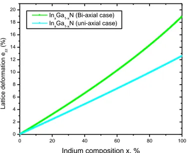
La composition des couches est déterminée par une observation MET haute résolution en coupe dans les conditions 2 ondes hors axe. La méthode d’analyse de la phase géométrique est utilisée pour l’interprétation des images MET. Cependant, cette méthode est relativement limitée pour la détermination des déformations à l’interface entre différentes couches. Afin d’éviter toute ambiguïté due à l’utilisation de cette méthode, la déformation moyenne de la couche d’InGaN par rapport à la couche de GaN a été systématiquement déterminée au centre des couches. Néanmoins, afin de relier la déformation des couches à leur composition, il est nécessaire de connaître de façon précise l’état de déformation de l’échantillon MET. En effet, l’état de contrainte dépend de l’épaisseur de l’échantillon dans la direction du faisceau électronique. Ainsi, selon que l’état de contrainte soit bi-axial, uni-axial ou intermédiaire, la détermination de la composition conduira, pour une même valeur de la déformation, à des valeurs de composition différentes. Afin d’éliminer toute incertitude liée à l’état de contrainte, plusieurs régions d’un même puits quantique ont été sondées de façon à vérifier que la déformation ne varie pas significativement. D’après ces observations, l’état de contrainte des échantillons est exclusivement bi-axial. Les compositions des puits ont donc été déterminées par la méthode correspondant à cet état de contrainte. De plus, nous avons simulé et comparé les valeurs moyennes d’épaisseur et de composition obtenues par analyse MET et par diffraction des rayons X sur la raie (0002) de façon à confirmer la pertinence de notre approche. D’après les analyses MET, nous avons obtenu la confirmation que les paramètres de croissance utilisés pour la couche d’encapsulation n’ont d’impact que sur l’épaisseur du puits, et non sur la composition déterminée au centre de celui-ci. Cette approche nous a également permis d’observer une éventuelle variation de la composition entre différents puits quantiques d’une même structure.
L’analyse des propriétés structurales des échantillons a permis d’observer des défauts tels que des dislocations coin supplémentaires et des défauts en forme de V générés dans les puits quantiques de certains échantillons. L’origine et l’impact de ces défauts ont été étudiés. Les observations ont montré que seuls les échantillons contenant des puits InGaN/GaN avec une fraction élevée d’Indium (≥ 18 %) et une épaisseur importante (≥ 3.5 nm) contiennent des dislocations traversantes de type <a> additionnelles générés au niveau des puits quantiques. Ces dislocations participent à la formation de défauts de type V au sein de la structure. D’après nos observations, ces dislocations ne sont pas créées à partir de fautes d’empilement ou à partir d’interfaces, mais pourraient être générées lorsque des défauts de type V atteignent l’interface entre deux couches.
Nous avons observé que de telles dislocations apparaissent sous la forme d’agrégats et qu’elles ne sont pas systématiquement générées à partir de dislocations traversantes déjà existantes. Au contraire, elles ne se forment qu’à partir de certaines régions des puits quantiques. Ainsi,
viii
nous proposons l’hypothèse selon laquelle l’origine de ces dislocations réside dans la formation d’agrégats d’Indium et/ou de défauts ponctuels au sein du puits quantique d’InGaN. Nous avons cherché une validation qualitative de cette hypothèse à partir d’images en champ sombre annulaire aux grands angles prises au niveau ou à proximité de ces défauts. Cependant, nous n’avons pu obtenir de preuve suffisamment convaincante de la présence d’agrégats d’indium dans nos structures. Il est possible que ces agrégats soient de tailles trop petites (nanométriques ou inférieur au nanomètre) pour être détectés par cette méthode.
La cartographie de l’espace réciproque par diffraction des rayons X sur les échantillons a permis de conclure que la présence de tels défauts ne permet pas de relaxer significativement la contrainte des couches épitaxiées. En effet, le taux de relaxation déterminé pour ces structures est faible, de l’ordre de 0.02 à 0.03 %. Par conséquent, la force motrice de la formation de ces dislocations ne peut pas être la relaxation de la contrainte due aux différences de paramètres de maille. Cependant, ces défauts se sont avérés néfastes pour l’efficacité de la photoluminescence des puits quantiques InGaN/GaN mesurée à température ambiante.
Une diminution de la densité de dislocations a été observée lorsque la température de croissance de l’InGaN est augmentée. Cela a pour conséquence la réduction de la composition en Indium dans le puits qui émet ainsi à une longueur d’onde plus courte. Une solution afin de compenser cet effet indésirable consisterait à épaissir le puits. Cependant, ceci n’est pas une solution idéale car la force de l’oscillateur est réduite lorsque l’épaisseur du puits augmente, du fait de l’effet Stark confiné quantique. Il a également été observé que l’encapsulation de l’InGaN par une couche d’AlGaN avec un taux d’Aluminium relativement élevé (environ 10 %) et épais (environ 3 nm) augmente le champ électrique interne dans la région du puits. Par conséquent, l’émission à des longueurs d’onde plus longues est favorisée mais l’efficacité quantique interne s’en trouve diminuée, à cause de l’effet Stark confiné quantique. En revanche, l’évolution de l’efficacité de la photoluminescence de puits InGaN encapsulés par une couche d’AlGaN en fonction de sa composition et de son épaisseur est moins évidente. Ainsi, l’optimisation de l’efficacité de la photoluminescence mesurée à température ambiante passe par un compromis entre ces différents paramètres : la qualité cristalline de l’InGaN (la température de croissance), l’épaisseur des puits, la composition de l’AlGaN, son épaisseur et ses conditions de croissance.
En conclusion, ce travail de thèse démontre qu’il n’existe pas de solution idéale permettant de concevoir des puits quantiques efficaces émettant dans les longueurs d’onde couvertes par le jaune et le vert. Ceci provient du fait que les différents paramètres régissant l’efficacité quantique interne interagissent négativement entre eux. Cependant, grâce au travail réalisé, des pistes d’améliorations ont été identifiées afin de parvenir à un compromis entre ces différents paramètres.
ix
Table of contents
Acknowledgements ... i
Abbreviations ... iii
Résumé ... v
Introduction ... 1
Introduction (French) ... 7
Chapter 1 ... 15
Fundamentals of nitride semiconductors ... 15
Introduction ... 15
1.1 Structural properties ... 15
1.1.1 Wurtzite structure ... 15
1.1.2 Relation between lattice constant and band gap energy ... 19
1.2 Dislocation basics ... 20
1.2.1 Slip plane system in wurtzite crystal structure ... 21
1.2.2 Dislocation types ... 22
1.3 Misfit in group III-nitride hetero-structures ... 23
1.3.1 Crystal deformation: bi-axial and uni-axial case ... 24
1.4 Spontaneous and piezoelectric polarization ... 29
1.4.1 Effects of polarization on (In,Ga)N/GaN heterostructure ... 31
1.4.1.1 Electric field in InGaN/GaN quantum wells ... 31
1.4.1.2 Effect of electric field on the InGaN quantum well transition energies ... 34
1.4.1.3 Impact of electric field on the radiative efficiency of InGaN/GaN QWs ... 35
1.5 Growth processes of LED structure ... 36
1.5.1 Metal-organic chemical vapor deposition (MOCVD) technique ... 37
1.5.2 The light emitting diode (LED) structure for light converter ... 38
Summary ... 39
Chapter 2 ... 43
x
Introduction ... 43
2.1 Phase diagram: phase separation of indium ... 44
2.2 Relaxation processes in InGaN/GaN system ... 47
2.2.1 Relaxation process through glide of dislocation ... 47
2.2.1.1 Matthews and Blakeslee model ... 48
2.2.1.2 Energy balance model ... 50
2.2.1.3 Critical thickness ... 51
2.2.1.4 Limitations of Matthews-Blakeslee and energy balance model ... 53
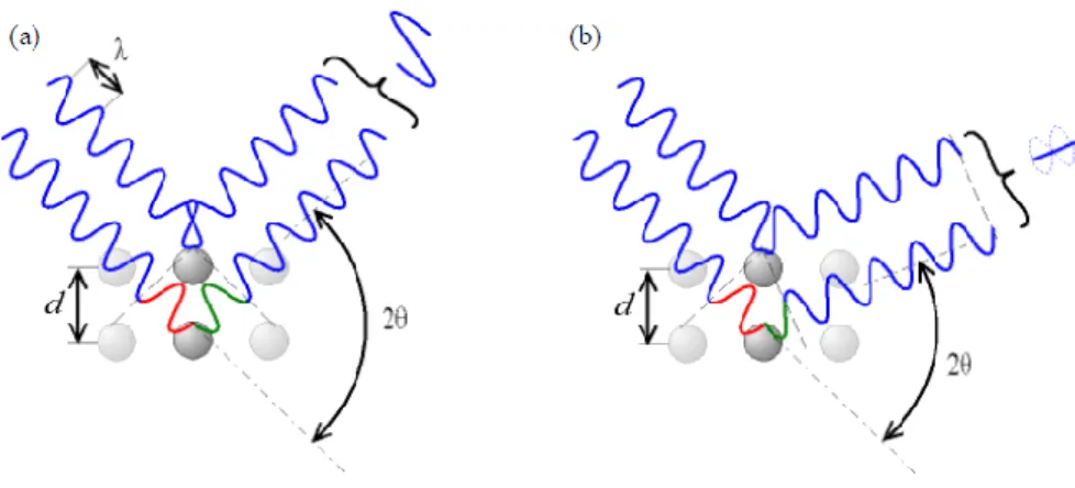
2.2.2 Relaxation process through generation of V defects ... 54
2.2.2.1 Shape and size of the V-defects ... 56
2.2.3 Other relaxation processes observed in wurtzite crystal structure ... 58
2.3 Quantum well thickness variation ... 58
2.4 LED performance due to these basic characteristics ... 60
Summary ... 63
Chapter 3 ... 67
Different characterization techniques ... 67
Introduction ... 67
3.1 High resolution scanning /transmission electron microscopy (HR-S/TEM) ... 68
3.1.1 Principle of HRTEM: scattering and diffraction ... 69
3.1.2 Basic operational modes in TEM: Diffraction and image modes ... 73
3.1.2.1 Different imaging techniques: bright field (BF) and dark field (DF) imaging .. 75
3.1.2.2 Dark field image techniques: strong beam dark field (SBDF) and weak beam dark field (WBDF) ... 77
3.1.3 Scanning transmission electron microscopy (STEM) ... 78
3.1.4 High angle annular dark field (HAADF) imaging ... 81
3.2 Determination of structural properties through HRTEM imaging techniques ... 82
3.2.1 Layer thickness measurement procedure ... 83
3.2.2 Indium composition determination within the InGaN layers ... 86
3.2.2.1 Off-axis two beam conditions in TEM ... 89
xi
3.2.3 Dislocation analysis through TEM ... 93
3.2.3.1 Extinction principle of dislocation contrast ... 94
3.3 X-ray diffraction ... 97
3.3.1 Working principle of XRD ... 97
3.3.2 X-ray diffraction analysis of multilayer epitaxy ... 99
3.3.2.1 The ω-2 scan ... 99
3.3.2.2 Reciprocal space map (RSM) ... 103
3.4 Room temperature photoluminescence ... 104
3.4.1 Experimental setup and measurement ... 105
3.5 Atomic force microscope ... 107
Summary ... 110
Chapter 4 ... 113
Study of the impact of capping processes for InGaN quantum wells ... 113
Introduction ... 113
4.1 The growth process of the samples in MOCVD reactor ... 114
4.2 Study of InGaN/GaN structure without any capping layers (sample 1 and 2) ... 116
4.2.1 The growth processes of sample 1 and 2 ... 116
4.2.2 Structural and optical properties of the first sample series (sample 1 and 2) ... 117
4.2.2.1 AFM analysis ... 117
4.2.2.2 TEM and XRD analysis ... 118
4.2.2.2.1 Dislocation analysis of samples 1 and 2 ... 120
4.2.2.2.2 Room temperature photoluminescence (RT-PL) analysis ... 122
4.3 Study of InGaN/GaN structure with AlGaN capping layer (sample A to D) ... 123
4.3.1 Growth process of samples A to D ... 124
4.3.2 Structural and optical properties of the second sample series (samples A to D) 125 4.3.2.1 AFM analysis ... 125
4.3.2.2 TEM and XRD analysis of the sample series ... 126
4.3.2.2.1 Dislocation analysis of samples A to D ... 132
4.3.2.3 Room temperature photoluminescence (RT-PL) analysis ... 134
xii
4.4.1 The growth processes of samples X to Z... 135
4.4.2 Structural and optical properties of the last sample series (samples X to Z) ... 136
4.4.2.1 AFM analysis ... 136
4.4.2.2 TEM and XRD analysis ... 137
4.4.2.2.1 Dislocation analysis of samples X to Z ... 139
4.4.2.3 Room temperature photoluminescence (RT-PL) analysis ... 141
4.5 Strain state of some samples of the studied series ... 142
4.6 Discussion ... 143
4.6.1 Strain relaxation ... 143
4.6.1.1 V-defects and additional threading dislocations ... 143
4.6.1.2 Inclined threading dislocation ... 145
4.6.2 Indium clustering ... 149
4.6.3 QW thickness increment ... 150
4.6.4 QW thickness variation ... 152
4.6.5 Impact of AlGaN capping layer deposition ... 153
Summary ... 153
Conclusion and perspective ... 157
Conclusion et perspective ... 161
1
Introduction
In mid-90’s, the first commercialization of white light emitting diode (LED) fabricated from the blue LED chips combined with yellow phosphors-cerium doped yttrium aluminium garnet (YAG) draws the attention of many researchers and scientists for the improvement of such novel devices1,2. Since then huge progress has been made in terms of efficiencies and recently record efficiencies of exceeding 200 lm/W are reported from such devices3,4. Figure 1 schematically shows the structure of such a white light emitting diode and its light generation process in forward bias. However, phosphor-converted white LED suffers from some intrinsic problems such as color instability with time and temperature, the additional process of phosphors on top of blue LED chips complicate the LED manufacturing process, which in turn increases the production complexities and cost of such devices.5
Figure 1: (a) The schematic diagram of a white light emitting diode and (b) the generation process of white light where the chip acts as a blue light source and the yellow phosphor as a light converter.3
To avoid the YAG phosphors covering process, wafer bonding of a blue (Al,Ga,In)N LED to a red (Al,Ga,In)P LED has been proposed to have the white light6. It has been also proposed to have CdSe/ZnS quantum dots (QDs) or (Al,Ga,In)P layers as semiconductor light converters to replace the YAG phosphor covering process for white LEDs7,8,9,10. But these approaches consist of adding foreign materials to the (Al, Ga, In)N material blue LED system, which complicates the overall white LED growth processes anyway.
Thus some research groups are working to realize “monolithic” or “phosphor free” white LEDs to overcome these difficulties11,12,13,14,15,16,17,18,19,20,21,22,23,24,25. Group III- nitride semiconductors play an important role in realizing such devices as their emission capability is also in the visible spectrum range26. The basic idea of such an approach is either to mix two or more color light emitting quantum wells (QWs) inside a p-n junction of an LED structure11-19 or to construct a blue-violet LED as pump source on top of a light converter emitting at higher wavelength
2
(green-yellow) to get the white light20-25. Both these approaches have been demonstrated in our lab. For example, in 2001, the first monolithic white light emitting diode (WLED) was demonstrated by mixing the blue and the yellow quantum wells inside a p-n junction11 and in 2006, the concept of pump-converter structure was proposed and a patent (French patent no. 06/50842) was made for combining a blue InGaN/GaN QW LED and a light converter (typically blue to yellow) based on stacking of nitride quantum dots or quantum wells (Al,Ga,In)N for white LED. Later in 2008, a blue LED grown on top of a yellow-green light converter was demonstrated to have a monolithic white LED.20 Figure 2 schematically illustrates both approaches and presents the advantage of avoiding the process complexities associated with phosphor-based white LEDs.
Figure 2: Schematic diagram of a (a) two different color light emitting quantum wells inside a p-n junction of a light emitting diode (LED) structure and (b) light pump-converter approach to obtain a
monolithic white light emitting diode (WLED).11,20,21
However, in the first approach of monolithic white LEDs (Figure 2 (a)), crucial problems of non-uniform carrier injection among the different active QWs and ensuing strong dependence of chromaticity coordinates on the injection current level exist for the device13 , whereas, in the second approach (Figure 2 (b)), such a carrier injection problem does not occur as the pump source excites the light converter optically to have a higher wavelength emission20-25. Moreover, the light converter with multiple quantum well (MQWs) structure helps to have less carrier density inside each QW of the light converter than that of current injected monolithic white LEDs, which limits the impact of efficiency droop at large operating current densities21,25. Yet, some additional drawbacks exist with these approaches as the reported efficiencies of monolithic white LEDs are still lower than that of standard phosphor based white LEDs12,27 and
3
it is believed that it is due to low internal quantum efficiency (IQE) of the green-yellow InGaN QWs. Thus in this work, we are going to focus on the structural and optical properties of these green-yellow InGaN QWs where they act as light converter in a monolithic white light emitting diode.
We know that the fabrication of an efficient, high brightness InGaN/GaN green-yellow light converter requires incorporating a high indium composition (>15%) within InGaN active quantum well (QW) region with reasonable well width thickness, LQW (2-4 nm). But the
fabrication of such high indium concentration InGaN layers by hetero-epitaxial growth processes is a very challenging task as the growth temperature of the InGaN well layer is much lower (700-800°C) than that of GaN barrier layer (900-1100°C), which induces different structural defects like QW thickness variation, point defects (vacancies, anti-sites) and Indium clustering28 due to low thermal stability of InGaN alloys29,30,31. In addition, the growth of the pump LED (blue-violet) structure along with P-GaN layer for electrical contact on top of light converter may degrade the InGaN QWs inside the light converter due to high temperature32,33,34. Again, depositing high indium composition InGaN layer on GaN layer induces large compressive stress within the epilayer due to a large lattice mismatch, which can lead to additional defect formation like V-pits, misfit and threading dislocations to release the accumulated stress energy35,36,37.
These structural defects are thought to be the prime reasons for inefficient InGaN quantum wells for green-yellow light converter. Moreover, if these additional structural defects are generated while growing a green-yellow MQW structure, then they will have a detrimental impact on the performance of the pump LED, as it is grown on top of the structure, and the overall performance of the targeted monolithic white LEDs will deteriorate.
Thus the structural and optical properties of a green-yellow MQW structure are very important issues to look at for better understanding of the behavior and the performance of monolithic white LEDs.
In this work, initially we have grown 10 periods of InGaN/GaN wurtzite MQW structures by changing the growth temperature and time of the QW layers. Later several structures with at least 10 periods of InGaN/AlGaN/GaN wurtzite MQWs are grown by metal-organic chemical vapor deposition (MOCVD) hetero-epitaxial growth process in order to achieve high brightness green, yellow-green MQW structures. In case of InGaN/AlGaN/GaN structures, after each InGaN QW layer growth, a few monolayers of AlGaN (less than 2 nm) are deposited as a capping layer before growing the GaN barrier layers within the structure. The deposition processes of AlGaN as capping layers have been modified among different studied samples. The purpose of this work is to study the impact of AlGaN capping layers and its growth processes on the structural and optical properties of such light converters. Finally, a comparative study has been made
4
between samples with several nm thick AlGaN capping layers (more than 2 nm) to that of low temperature GaN capping layers on top of InGaN QWs of a light converter structure.
In studying the structural properties, we are concerned about measuring precisely the different layer thicknesses, indium compositions within the active regions, along with identifying the different types of defects present in the grown structures. This structural information is obtained mainly from image analysis processes used in transmission electron microscopy (TEM) technique. Moreover, to confirm and verify the obtained data from TEM analysis, we conducted the X-ray diffraction (XRD) of each sample. The overall surface morphology of different samples is also observed with the help of atomic force microscopy (AFM). By analyzing this structural information of the corresponding samples, we tried to correlate them to that of their optical properties measured by room temperature photoluminescence (RTPL).
The studied results are presented in this manuscript which is organized in the following manner:
In chapter 1, we introduce the fundamental structural properties of group III-nitrides of wurtzite crystal structure. Then the slip plane systems along with different types of dislocations associated with such crystal structure are discussed. Later, the stress-strain relationship induced in the epitaxial layer and its impact on optical properties of the material is highlighted. A brief description of the metal organic chemical vapor deposition (MOCVD) technique and the studied samples structure are included.
Chapter 2 deals with the fundamental characteristics involved with InGaN/GaN hetero-structures. An overview of different characteristics such as phase separation, different relaxation processes and layer thickness variation observed with high indium composition InGaN layers of InGaN/ GaN system is presented. The performances of light emitting diodes (LEDs) due to these characteristics are also discussed in brief.
In chapter 3, we focus on the basics behind the experimental techniques that are used in this work. We are going to present the particular experimental methods with the goal of highlighting how and why we utilize these tools to determine the targeted properties of our studied samples. The advantage and disadvantage of these experimental procedures are also discussed in different subsections of the chapter.
In final chapter 4, we present the obtained results of our work: the importance of the deposition of AlGaN as capping layers, the best growth process to compensate the InGaN QW thickness variation, the indium clustering, segregation and/or evaporation due to high temperature processing involved with InGaN/GaN LED system, and the associated optical
5
properties of the samples are presented in the chapter. Moreover, additional dislocations are found with very high Indium composition (≥ 20%) InGaN layers, so we are going to discuss the type of such additional dislocations and try to identify their origin within the InGaN layer in the chapter.
7
Introduction (French)
Dans le milieu des années 90 ont été commercialisées les premières diodes électroluminescentes (DELs) blanches. Ces dernières sont fabriquées à partir DELs bleues combinées avec du phosphore cérium jaune dopé avec du grenat d’yttrium et d’aluminium (YAG). Dès lors, l’amélioration de tels dispositifs optiques a suscité l’engouement de la communauté scientifique1,2. Des progrès importants ont été reportés ces dernières années avec l’obtention de records d’efficacités pour ces dispositifs DELs dépassant les 200Im/W 3,4. La Figure 1 montre schématiquement le fonctionnement d’une structure DEL blanche et son processus de génération de lumière en polarisation directe. Cependant les DELs dont la couleur blanche est obtenue à l’aide de phosphore souffrent de problèmes intrinsèques comme l’instabilité de la couleur au cours du temps et lorsque la température varie. Les processus permettant l’addition de phosphores sur les puces des DELs bleu ajoutent aussi des complications lors de la fabrication qui vont augmenter la complexité de production et le prix de ces dispositifs.5
Figure 1: (a) Le schéma de principe d'une diode électroluminescente blanche et (b) le processus de génération de lumière blanche où les puces joue le rôle de source de lumière bleue et le
phosphore jaune celui de convertisseur de lumière.3
Pour éviter le procédé de recouvrement par les phosphores YAG, le collage des supports des DELs bleu (Al,Ga,In)N avec des support de DELs rouge (Al,Ga,In)P a été proposé pour obtenir de la lumière blanche6. Il a aussi été proposé d’utiliser, pour l’obtention de DELs blanches, des boites quantiques (BQs) de CdSe/ZnS ou des couches de (Al,Ga,In)P comme convertisseurs de lumière à base de semi-conducteur afin de remplacer les procédés de recouvrement par phosphores YAG 7,8,9,10. Mais ces approches impliquent l’addition de matériaux étrangers à la filière nitrure (Al,Ga,In)N dont sont constitués les DELs bleu. Cela complique le processus global de la croissance des DELs blanches.
En conséquence, pour dépasser ces problèmes, certains groupes de recherches concentrent leurs efforts sur la réalisation de DELs blanches dites «monolithiques» ou « sans phosphore »
11,12,13,14,15,16,17,18,19,20,21,22,23,24,25
8
d’éléments III de la classification périodique joue un rôle important dans la réalisation de ces dispositifs du fait que leur émission lumineuse se trouve aussi en partie dans la zone spectrale du visible26. L’idée sur laquelle repose cette approche est de mélanger deux ou plusieurs couleurs d’émissions lumineuses issues des puits quantiques dans la jonction p-n d’une structure DEL11-19 .On peut aussi de manière complémentaire construire une DEL bleu-violet comme source de pompage optique au-dessus d’un convertisseur de lumière émettant à des longueurs d’ondes plus élevées (vert-jaune) afin d’obtenir de la lumière blanche20-25.
Ces deux méthodes ont été démontrées dans notre laboratoire. Par exemple en 2001, la première diode électroluminescente monolithique blanche a été réalisée en mélangeant à l’intérieur d’une jonction p-n des puits quantiques possédant des longueurs d’ondes d’émissions dans le bleu et dans le jaune11. Un autre exemple est en 2006, le dépôt d’un brevet (brevet Français numéro 06/50842) sur la réalisation de DELs blanches. Le concept repose sur la conversion de lumière par pompage optique afin de combiner une DEL émettant dans le bleu (puits quantiques InGaN/GaN) avec un convertisseur de lumière (typiquement du bleu au jaune) constitué de l’empilement de boites quantiques ou de puits quantiques de nitrures (Al,Ga,In)N. Ensuite, en 2008, une DEL bleue déposée au-dessus d’un convertisseur de lumière jaune-vert a été démontrée afin d’obtenir une DEL blanche monolithique20. La figure 2 illustre schématiquement ces approches qui présentent l’avantage d’éviter la complexité des procédés associés à la réalisation des DELs blanches issues de la conversion des DELs bleues avec des phosphores.
Figure 2: Schéma d'une DEL présentant (a) deux couleurs de lumière différentes émises par des puits quantiques à l'intérieur d'une jonction p-n formant la zone active d’une diode électroluminescente (DEL) et (b)l’ approche de conversion par pompage optique pour obtenir
9
Cependant, dans la première approche de DEL blanche monolithique (Figure (2a)), des problèmes cruciaux ont été mis en lumière concernant la non-uniformité de l’injection des porteurs de charges à travers les différents puits quantiques constituant la zone active. Une des principales conséquences étant une forte dépendance des coordonnées chromatiques en fonction du courant d’injection dans le dispositif13.
Dans le cas de la seconde approche (Figure (2b)), ce problème lié à l’injection des porteurs de charges n’a pas lieu d’être car la source de pompage optique excite optiquement le convertisseur de lumière pour avoir une émission dans des longueurs d’ondes plus élevées20-25. De plus, le convertisseur de lumière avec une structure de multi-puits quantiques (MPQs) contribue à la présence d’une densité de porteurs de charges plus faible dans chacun des PQ du convertisseur de lumière qu’avec des DELs blanches monolithiques injectées électriquement. Cela limite la chute de l’efficacité lors d’un fonctionnement à des larges densités de courants21,25.
Cependant, quelques désavantages liés à ces approches persistent. En effet les efficacités démontrées pour des DELs blanches monolithiques restent plus faibles que celles des DELs blanches standards à base de phosphore12,27 . Cela est dû à une plus faible efficacité quantique interne (EQI) des boites quantiques à base d’InGaN émettant de la lumière dans le domaine spectral vert-jaune. En conséquence, dans cette étude nous allons nous concentrer sur les propriétés structurales et optiques de ces puits quantiques InGaN émettant dans le vert-jaune où elles vont jouer le rôle de convertisseur de lumière pour la réalisation de DELs blanches monolithiques.
Nous savons que la fabrication d’un convertisseur de lumière InGaN/GaN vert-jaune efficace nécessite l’incorporation d’une composition élevée d’indium (>15%) dans les zones actives composées de puits quantiques d’InGaN. De plus, ces derniers doivent aussi avoir une largeur raisonnable, LPQ (2-4nm). Mais la fabrication de couches d’InGaN possédant une importante
concentration d’indium n’est pas facile à réaliser en raison du fait que la température de croissance des puits d’InGaN doit être beaucoup plus faible (700-800°C) que celle de la couche barrière en GaN (900-1100°C). Cette différence de température de croissance induit des défauts structuraux tels que l’ondulation de l’épaisseur des PQs InGaN, des défauts ponctuels (lacunes, anti-site) et de la ségrégation d’indium28 due à la faible stabilité thermique des alliages InGaN29,30,31.
En outre, la croissance de la structure de pompage optique (bleu-violet) de la DEL, ainsi que la croissance de la couche p-GaN servant pour le contact électrique au-dessus du convertisseur de lumière risquent éventuellement, en raison des températures de croissances importantes utilisées,32 de détériorer les puits quantiques en InGaN qui sont situés à l’intérieur du convertisseur de lumière,33,34.
Par ailleurs, la déposition d’une couche en InGaN avec une forte concentration d’indium sur une couche de GaN entraine une large contrainte compressive dans la couche épitaxiée en raison de la grande différence de paramètre de maille. Cela peut conduire à la formation de
10
défauts additionnels. La formations de ces defauts permet de diminuer l’energie issue de la contrainte accumulée35,36,37.
Ces défauts structuraux sont probablement identifiés comme la cause principale de l'inefficacité des puits quantiques InGaN vert-jaune qui composent le convertisseur de lumière. Par ailleurs, si ces défauts structuraux supplémentaires sont générés lors de la croissance d'une structure MPQs vert-jaune, alors ils auront aussi un impact négatif sur la performance de la DEL de pompage. En effet, cette dernière est déposée sur le dessus de la structure précédente, par conséquent la performance globale de la DEL blanche monolithiques finale va se détériorer. Ainsi, en définitive les propriétés structurales et optiques des MPQs vert-jaune sont un sujet d’étude dont l’approfondissement est crucial pour améliorer notre compréhension du comportement et des performances des DELs blanches monolithiques.
Dans cette étude, nous avons initialement déposé 10 périodes d’empilement wurtzite InGaN/GaN en changeant la température et la durée de croissance des puits quantiques. Ensuite plusieurs structures avec au moins 10 périodes de MPQs wurtzite InGaN/AlGaN/GaN ont été déposées heteroepitaxialement. La technique d’épitaxie utilisée est l’épitaxie en phase vapeur aux organométalliques (EPVOM) dans le but d’obtenir des MPQs vert, jaune-vert présentant une forte émission lumineuse. Dans le cas de l’empilement InGaN/AlGaN/GaN, après chaque croissance de couche de PQ InGaN, quelques monocouches atomiques de AlGaN (<2nm) ont été déposées comme couche de protection avant la croissance de la couche barrière en GaN. Les processus de croissance de ces couches de protection en GaN ont été explorés à travers les différents échantillons étudiés.
L’objectif de ce travail de thèse est d’étudier l’impact de la couche de protection en AlGaN ainsi que de son processus de croissance sur les propriétés structurales et optiques du convertisseur de lumière situé au-dessus des PQs InGaN. Enfin, différents échantillons avec différentes épaisseurs de couche de protection AlGaN (>2nm) ont été étudiés de manière comparative avec d’autres types d’échantillons utilisant une couche de GaN déposé à basse température comme couche de protection au-dessus du convertisseur de lumière.
Concernant l’étude des propriétés structurales, nous nous sommes particulièrement intéressés aux mesures précises des épaisseurs des couches, des compositions en indium dans les zones actives ainsi qu’à l’identification des différents types de défauts présents dans les structures déposées. Ces informations structurales ont été étudiées principalement à partir de processus d’analyses d’images obtenues à l’aide d’un microscope électronique à transmission (MET). Par ailleurs, pour confirmer et vérifier les résultats issus de l’analyse MET, nous avons mené des analyses de diffraction par Rayons X (DRX) sur chaque échantillon. La morphologie de surface a aussi été observée à l’aide d’un microscope à force atomique (AFM). Et finalement nous avons essayé de relier ces informations structurales aux propriétés optiques mesurées par photoluminescence à température ambiante.
Les résultats obtenus lors de cette étude sont présentés dans ce manuscrit de la manière suivante :
11
Dans le chapitre 1, nous introduirons les propriétés structurales fondamentales des cristaux wurtzite semi-conducteurs composés III-nitrure. Ensuite nous discuterons les systèmes de plans de glissements de cette structure wurtzite ainsi que des différents types de dislocations associées. La relation contrainte déformation dans la couche épitaxiée et son influence sur les propriétés optiques du matériau seront mises en évidence. Enfin nous décrierons brièvement la technique de dépôt par EPVOM et la structure de l’empilement des échantillons étudiés. Le chapitre 2 traite des caractéristiques fondamentales impliquées dans l’heterostructure InGaN/GaN. Une vue d’ensemble des différentes caractéristiques associées aux couches InGaN possédant une forte concentration d’indium dans le système d’empilement InGaN/GaN seront présentées. Nous nous attarderons principalement sur la séparation de phase, les processus de relaxation et le phénomène d’ondulation des épaisseurs des couches. Enfin nous discuterons brièvement au sujet de l’impact de ces différentes caractéristiques structurales sur les performances des diodes électroluminescentes (DELs).
Dans le chapitre 3, nous nous concentrerons sur les principes de bases sur lesquels reposent les techniques expérimentales que nous avons utilisées lors de ce travail de thèse. Nous présenterons certaines méthodes expérimentales en particulier afin de mettre de mettre en évidence comment et pourquoi ces outils de caractérisations peuvent être utilisés pour déterminer précisément les propriétés de nos échantillons. Les avantages et désavantages de ces procédures expérimentales serons aussi discutés dans les différentes sous-sections de ce chapitre.
Dans le chapitre 4, dernier chapitre de ce manuscrit, nous présenterons les résultats obtenus au cours de ce travail de thèse, à savoir:
L’importance de la déposition de la couche de protection en AlGaN. Les meilleures conditions de croissances pour compenser l’ondulation de l’épaisseur des PQs en InGaN. La formation d’îlots d’indium, la ségrégation et/ou l’évaporation due à la température élevée utilisée lors de la réalisation de DELs composées d’empilement de type InGaN/GaN. Les propriétés optiques associées à ces échantillons seront présentées dans ce chapitre. De plus, des dislocations supplémentaires ont été mises en évidence dans les couches en InGaN possédant des compositions en indium très élevés (>20%). Nous discuterons donc dans ce chapitre du type de ces dislocations additionnelles et nous tenterons de définir leur origine.
Finalement, une conclusion générale ainsi que les perspectives de cette étude seront présentées.
References:
1Kanji BANDO, Kensho SAKANO, Yasunobu NOGUCHI, and Yoshinori SHIMIZU, Journal of Light and Visual Environment 22 (1), 2 (1998).
2
12
3
Narukawa Yukio, Ichikawa Masatsugu, Sanga Daisuke, Sano Masahiko, and Mukai Takashi, Journal of Physics D: Applied Physics 43 (35), 354002 (2010).
4
Narukawa Yukio, Sano Masahiko, Ichikawa Masatsugu, Minato Shunsuke, Sakamoto Takahiko, Yamada Takao, and Mukai Takashi, Japanese Journal of Applied Physics 46 (10L), L963 (2007).
5
M. Meneghini, A. Tazzoli, G. Mura, G. Meneghesso, and E. Zanoni, Electron Devices, IEEE Transactions on 57 (1), 108 (2010).
6
X. Guo, G. D. Shen, B. L. Guan, X. L. Gu, D. Wu, and Y. B. Li, Applied Physics Letters 92 (1), 013507 (2008).
7
Chen Horng-Shyang, Yeh Dong-Ming, Lu Chih-Feng, Huang Chi-Feng, Wen-Yu Shiao, C. C. Yang, I. S. Liu, and Su Wei-Fang, Photonics Technology Letters, IEEE 18 (13), 1430 (2006).
8
S. Nizamoglu, T. Ozel, E. Sari, and H. V. Demir, Nanotechnology 18 (6), 065709 (2007).
9
Ho Seong Jang, Byoung-Hwa Kwon, Heesun Yang, and Duk Young Jeon, Applied Physics Letters
95 (16), 161901 (2009).
10
Xiaoyun Guo, John W. Graff, E. F. Schubert, and Jr Robert F. Karlicek, 2000 (unpublished).
11
Damilano Benjamin, Grandjean Nicolas, Pernot Cyril, and Massies Jean, Japanese Journal of Applied Physics 40 (9A), L918 (2001).
12
Yamada Motokazu, Narukawa Yukio, and Mukai Takashi, Japanese Journal of Applied Physics 41 (3A), L246 (2002).
13
S. Dalmasso, B. Damilano, C. Pernot, A. Dussaigne, D. Byrne, N. Grandjean, M. Leroux, and J. Massies, physica status solidi (a) 192 (1), 139 (2002).
14
S. J. Chang, L. W. Wu, Y. K. Su, C. H. Kuo, W. C. Lai, Y. P. Hsu, J. K. Sheu, J. F. Chen, and J. M. Tsai, Electron Devices, IEEE Transactions on 50 (2), 519 (2003).
15
A. Dussaigne, J. Brault, B. Damilano, and J. Massies, physica status solidi (c) 4 (1), 57 (2007).
16 Chi-Feng Huang, Chih-Feng Lu, Tsung-Yi Tang, Jeng-Jie Huang, and C. C. Yang, Applied Physics
Letters 90 (15), 151122 (2007).
17
Sung-Nam Lee, H. S. Paek, H. Kim, T. Jang, and Y. Park, Applied Physics Letters 92 (8), 081107 (2008).
18
Funato Mitsuru, Kondou Takeshi, Hayashi Keita, Nishiura Shotaro, Ueda Masaya, Kawakami Yoichi, Narukawa Yukio, and Mukai Takashi, Applied Physics Express 1 (1), 011106 (2008).
19
Lu Chih-Feng, Huang Chi-Feng, Yung-Sheng Chen, Wen-Yu Shiao, Cheng-Yen Chen, Yen-Cheng Lu, and Yang Chih-Chung, Selected Topics in Quantum Electronics, IEEE Journal of 15 (4), 1210 (2009).
20
B. Damilano, A. Dussaigne, J. Brault, T. Huault, F. Natali, P. Demolon, P. De Mierry, S. Chenot, and J. Massies, Applied Physics Letters 93 (10), 101117 (2008).
21
B. Damilano, P. Demolon, J. Brault, T. Huault, F. Natali, and J. Massies, Journal of Applied Physics
108 (7), 073115 (2010).
22
V. V. Nikolaev, M. E. Portnoi, and I. Eliashevich, physica status solidi (a) 183 (1), 177 (2001).
23
B. Damilano, N. Trad, J. Brault, P. Demolon, F. Natali, and J. Massies, physica status solidi (a) 209 (3), 465 (2012).
24
Damilano Benjamin, Kim-Chauveau Hyonju, Frayssinet Eric, Brault Julien, Hussain Sakhawat, Lekhal Kaddour, Vennéguès Philippe, Mierry Philippe De, and Massies Jean, Applied Physics Express 6 (9), 092105 (2013).
25
Dario Schiavon, Michael Binder, Andreas Loeffler, and Matthias Peter, Applied Physics Letters
102 (11), 113509 (2013).
26
Shuji Nakamura, Solid State Communications 102 (2–3), 237 (1997).
27
M. R. Krames, O. B. Shchekin, Regina Mueller-Mach, Gerd O. Mueller, Zhou Ling, G. Harbers, and M. G. Craford, Display Technology, Journal of 3 (2), 160 (2007).
13
28
S. Kret, F. Ivaldi, K. Sobczak, R. Czernecki, and M. Leszczyński, physica status solidi (a) 207 (5), 1101 (2010).
29
G. T. Thaler, D. D. Koleske, S. R. Lee, K. H. A. Bogart, and M. H. Crawford, Journal of Crystal Growth 312 (11), 1817 (2010).
30
M. S. Oh, M. K. Kwon, I. K. Park, S. H. Baek, S. J. Park, S. H. Lee, and J. J. Jung, Journal of Crystal Growth 289 (1), 107 (2006).
31
W. Lee, J. Limb, J. H. Ryou, D. Yoo, T. Chung, and R. D. Dupuis, Journal of Electronic Materials 35 (4), 587 (2006).
32
S. M. Ting, J. C. Ramer, D. I. Florescu, V. N. Merai, B. E. Albert, A. Parekh, D. S. Lee, D. Lu, D. V. Christini, L. Liu, and E. A. Armour, Journal of Applied Physics 94 (3), 1461 (2003).
33
Y.S. Lin, K. J. Ma, C. Hsu, Y.Y. Chung, C. W. Liu, S. W. Feng, Y. C. Cheng, C. C. Yang, M. H. Mao, H. W. Chuang, C. T. Kuo, J. S. Tsang, and T. E. Weirich, Applied Physics Letters 80 (14), 2571 (2002).
34
Y. Y. Chung, Y. S. Lin, S. W. Feng, Y. C. Cheng, E. C. Lin, C. C. Yang, K. J. Ma, C. Hsu, H. W. Chuang, C. T. Kuo, and J. S. Tsang, Journal of Applied Physics 93 (12), 9693 (2003).
35
H. K. Cho, J. Y. Lee, G. M. Yang, and C. S. Kim, Applied Physics Letters 79 (2), 215 (2001).
36
H. K. Cho, J. Y. Lee, C. S. Kim, and G. M. Yang, Journal of Applied Physics 91 (3), 1166 (2002).
37
Chapter 1
15
Chapter 1
Fundamentals of nitride semiconductors
Introduction
To study and understand the structural and optical properties of group III-nitrides LEDs, it is important to know some of their fundamental properties. Thus in this chapter, we present some basic structural information like lattice parameters, different crystallographic planes and directions of group III-nitride wurtzite crystals. Then the structural information is used to elaborate the idea of strain-stress relationship involved in group III-nitride hetero-epitaxial growth process.
The fundamentals of defects like dislocations involved in group III-nitride hetero-epitaxial growth are highlighted. The classification of the different types of dislocations and the different slip plane systems for the wurtzite crystal structure are introduced in this chapter.
Depending on the growth orientation of group III-nitride crystal structure, the induced strain in the epilayers has impact on their observed optical properties due to polarization fields involved within the structure. Thus the origin of these polarization fields and their effects are discussed. Finally, we discuss the basic mechanisms involved in metal organic chemical vapor deposition (MOCVD) growth technique and conclude our chapter by describing the structure of our studied samples in brief.
1.1 Structural properties
Group-III nitride materials can crystallize either in the cubic zinc-blende or the hexagonal wurtzite structure. The zinc-blende structure being meta-stable, the growth of high structural and optical quality group III-nitride crystals has been only achieved in the wurtzite phase. We are going to address the structural properties of wurtzite crystal structure in the next subsection.
1.1.1 Wurtzite structure
In order to emphasize the hexagonal symmetry of the wurtzite crystal structure, the directions in a hexagonal structure are described by four translational vectors rather than three vectors1. Figure 1-1 (a) shows a hexagonal unit cell with primary axes, where the x and y axes are at 120° to each other. Figure 1-1 (b), shows the problem that arises when expressing the same group of planes of the hexagonal system in 3 indexed {hkl}c representations. For example, all the prismatic planes parallel to the z-axis should have the same form of representation as they are crystallographically equivalent, but in case of 3 indexed notation system, their indices differ in
16
representation as shown in Figure 1-1 (b). To overcome this problem a fourth axis - the u axis - is introduced at 120° to both the x and y axes as shown in Figure 1-1 (c). Thus the indices of the lattice for wurtzite hexagonal structure are now consisting of four numbers (hkil). From vector summation, it is obvious that the sum of the unit distance along x, y and u axes should result to zero (i.e. a+b+t=0, from Figure 1-1 (c)), so the first three numbers in the Miller –Bravais indices should also become zero, i.e. h+k+i=0 or i=-(h+k). This condition allows us to represent the same group of planes of the hexagonal system with the combination of first three numbers of the four indexed notation (hkil), as shown for the six prismatic planes of the system {1-100} in Figure 1-1(c) without ambiguity. We are going to use the four-index notation to represent the directions and planes of our sample structure in the upcoming discussion, so for the convenience of the reader, we are summarizing the bracketing convention in Table 1-1 below.
Figure 1-1: a) Unit cell of the hexagonal lattice showing the arrangement of the atoms along with the primary axes. Projected view of the unit cell structure along z-axis, b) showing the traces of the six prism
faces indexed by 3 indexed system {hkl} and c) same planes indexed by Miller-Bravais (four-index) system2.
Table 1-1 Summary of bracketing convention for four index notation
The wurtzite structure has a hexagonal unit cell and each atom is in a sp3-hybridization state and bounded to four other atoms of different types. These four atoms are located at the corners of a tetrahedron. The atoms arrangement can be represented as two hexagonal close-packed sublattices shifted with respect to each other, forming a close-packing sequence of ABAB..type. The wurtzite structure symmetry is described by the P63mc space group. The
17
denoted as lattice parameter ‘a’ and the distance between the same types of atom along the perpendicular direction to that hexagonal plane is denoted as ‘c’ parameter of the structure. The axis along the hexagonal plane is considered to be a-axis and the perpendicular direction to that a-axis is known as c-axis of the wurtzite structure. The nearest distance between the two different atoms along the c-axis is denoted as ‘u’ and known as bond length. Figure 1-2 represents the atomic structure of GaN in the wurtzite structure. Here the bigger yellow balls and smaller gray ones are representing Ga atoms and N atoms, respectively, as Ga atoms have higher atomic mass than that of N atoms. The two tetrahedrons are also represented by shaded areas within the figure.
Figure 1-2: Atomic structure of GaN as wurtzite crystal. Ga atoms are represented in yellow color and are relatively larger than N atoms represented in gray. The bonds are presented in two colors. Lattice
parameters along with bond length are presented in blue arrows3.
The values of the lattice parameters for binary group III-nitride compounds are listed in Table 1-2, along with the ratio of the length of the c and a axes (axial ratio) and the bond length u and c axis4,5,6,7. Considering a hard sphere model as an ideal structure, where the bond length distance of the individual atoms is considered to be equal, the c/a ratio should have the value of 1.633. But the practical values of c/a ratio vary slightly as indicated in Table 1-2 due to the fact that the atomic distance between the two different atoms along the c axis is different from the ones outside the c axis.
18 Table 1-2: Lattice parameters and ratios for AlN, GaN and InN crystals in wurtzite phase
The wurtzite structure is non-centrosymmetric, i.e. the [0001] and directions are not equivalent. In wurtzite structure, the [0001] direction is defined as the pointing direction from III-metal atoms (Ga atoms) towards N atoms. Crystal grown along [0001] direction is known as Ga-face or metal polarity crystal and when the crystal is grown along the other direction, i.e., direction, it is called N polarity or N-face crystal. Figure 1-3 illustrates the two faces depending on the growth directions for GaN material.
Figure 1-3: Schematic illustration of a) Ga-polarity b) N-polarity along two opposite c-axis directions for GaN wurtzite structure8.
In this work, all the samples are grown along the [0001] polar direction and the samples are observed and images are analyzed using cross section transmission electron microscopy (cs-TEM) imaging technique. Indium composition within the active region, the types of dislocations and also the thickness of different regions of the sample structures are observed and analyzed by tilting the TEM samples along three principal zone axes as and , respectively. The details of the imaging processes and analysis techniques of TEM will be discussed later in chapter 3. The projection of the crystal structure along different zone axes has been schematically shown in Figure 1-4.
19 Figure 1-4: Projection of the GaN wurtzite crystal structure along a) , b) and c) zone axes for a Ga polarity structure where yellow balls are for Ga atoms and the blue ones
are for N atoms3.
1.1.2 Relation between lattice constant and band gap energy
The band gap energy Eg (eV) of group III-nitride materials can be related to their lattice constant
value (a0) as both the band gap energy and the lattice constant values varies according to
Vegard’s law, depending on the composition value (x). The lattice parameter (a0) of any ternary
nitride, for example, InxGa1-xN can be determined from Vegard’s law as follows:
(1.1)
where X and Y represent any of the two atoms from Al, Ga and In atoms and x corresponds to the ratio of composition within the alloy. From Table 1-2, the initial lattice constant value of binary compounds of group III-nitrides (i.e., AlN, GaN and InN) is used to interpolate the lattice constant values of other ternary alloy using equation 1.1. Similarly, the band gap energy Eg (eV)
of any ternary nitride can be interpolated using the Vegard’s law considering the initial band gap energy of the binary compound of group III- nitride (i.e., AlN, GaN and InN). Vurgaftman and Meyer9 reported the band gap energy for the binary compounds of group III-nitride (i.e., AlN, GaN and InN) at zero Kelvin (T=0K) temperature as shown in Table 1-3. But to correlate the theoretical10 and experimental11 values of the band gap energy Eg (eV) of a ternary alloy, an
additional term with a parameter b is considered as shown in equation 1.2. This parameter is known as bowing parameter.
(1.2)
20 Table 1-3: Band gap energies of group III- nitride binaries at 0 K9
Material InN GaN AlN
Structure Wurtzite Wurtzite Wurtzite
Band gap (eV) 0.78 3.51 6.0
Table 1-4: Bowing parameters of group III-nitride alloys9
Alloy AlGaN InGaN AlInN
Bowing parameter b (eV) 0.70 1.40 2.50
Now correlating the two equations 1.1 and 1.2, we can find the relation between the lattice constant (a0) and band gap energy (eV) of a ternary alloy. Figure 1-5 illustrates the lattice
constant a0 (in Å unit) value versus the band gap energy Eg (in eV unit) for group III- nitride
materials, where bowing parameters are neglected for simplicity. It is clear from Figure 1-5 that the InxGa1-xN alloy is a very important material as it covers entire visible spectrum range from
infra-red (IR) to ultra-violet (UV) depending on the Indium composition (x).
Figure 1-5: Graph of band gap energy vs. lattice constant for group III-nitride materials12.
1.2 Dislocation basics
The group III- nitride multiple quantum well (MQW) structure is generally developed on top of a few micrometer thick GaN epilayer which acts as a buffer layer as it is grown on top of a foreign substrate such as sapphire. Owing to low cost and large availability, sapphire is the mostly used substrate to grow group III-nitride heterostructures. The growth process of such GaN buffer layer on top of sapphire substrate is complicated and beyond the scope of this work. So the detailed growth mechanism of such buffer layer is not discussed. But due to the high lattice mismatch (~16%)13, structural differences and growth process mechanisms, the GaN buffer layer contains a high density of dislocations of about 5x10⁸ to 1x10⁹ per cm2, known as
pre-21
existing dislocations. In hetero-epitaxial growth, the dislocations thatpropagating through any grown epilayer are termed as threading dislocation (TD). Figure 1-6 shows a large cross sectional view of a sample, where the threading dislocations are easily seen in GaN buffer layer as indicated. It is important to know the type and the slip planes involved with these dislocations to better understand their propagation mechanism while growing the epitaxial layer. Thus in the next subsection we are going to discuss the type of dislocations and the slip plane system observed in group III-nitride wurtzite structures in brief.
Figure 1-6: Cross-sectional transmission electron microscope (cs-TEM) imaging along <1-100> zone axis, showing different regions of the sample along with the contrast for threading dislocations (TDs) as
indicated by white arrows for two. 1.2.1 Slip plane system in wurtzite crystal structure
A slip plane is defined as a plane which contains both the Burger vector b (it is defined as the dislocation-displacement vector of the crystal structure14,15) and the unit vector u (which is parallel to the dislocation line direction) of a dislocation. Moreover, a slip plane and a slip direction (Burger vector) constitute a slip system. In the wurtzite crystal structure possible slip planes and slip directions are indicated as shown in Figure 1-7, where the planes are in gray color and the probable slip directions within the planes are indicated by bold arrows. Depending on the planes of the hexagonal structure, slip plane system can be classified into three groups as:
Basal slip system which contains only {0001} basal plane and slip direction in the plane,
as shown in Figure 1-7(a): {0001} <11-20>.
Prismatic slip system which contains the families of prismatic planes as {1-100} and