HAL Id: dumas-01735579
https://dumas.ccsd.cnrs.fr/dumas-01735579
Submitted on 16 Mar 2018HAL is a multi-disciplinary open access archive for the deposit and dissemination of sci-entific research documents, whether they are pub-lished or not. The documents may come from teaching and research institutions in France or abroad, or from public or private research centers.
L’archive ouverte pluridisciplinaire HAL, est destinée au dépôt et à la diffusion de documents scientifiques de niveau recherche, publiés ou non, émanant des établissements d’enseignement et de recherche français ou étrangers, des laboratoires publics ou privés.
Improvement of the volume ramp up process
Antoine Mauduit
To cite this version:
Antoine Mauduit. Improvement of the volume ramp up process. Micro and nanotechnolo-gies/Microelectronics. 2016. �dumas-01735579�
Ecole d’ingénieurs eicnam
Improvement of the Volume Ramp Up process
Dossier de synthèse présenté par
Antoine, Serge, Pierre MAUDUIT
Pour obtenir
Le Diplôme d'ingénieur du CNAM Spécialité
mesure-analyse, parcours Instrumentation qualité
Travaux présentés le 21 juin 2016 devant le jury composé de M. Patrick Juncar Cnam PU Président Mme Annick Razet Cnam PU
M. Mark Plimmer MCF , Cnam
Mme Joanne Schel NXP Semiconductor M. Giacomo Pecoraro NXP Semiconductor
EiCNAM UASM32- 2015-2016 Antoine MAUDUIT
Improvement of the Volume Ramp Up Process 2
Résumé
La mise en production d’un circuit semi-conducteur est toujours une phase délicate. En effet, malgré toutes les étapes visant à qualifier le produit et les outils de test, le manque d’expérience sur le produit fait que les premières livraisons se font dans des conditions difficiles. C’est la capabilité des procédés de fabrication qui sont souvent en cause. Cela a pour conséquence que lorsque qu’une variation se produit sur un élément de la chaîne de fabrication, l’impact sur les performances peut s’avérer critique. Du fait que les rendements ne sont pas prévisibles, cela peut mener à des retards de livraisons. Ce qu’il faut savoir c’est que les procédés composant la chaîne de fabrication allant de la FAB à la livraison sont nombreux et les problèmes qui leur sont associés très spécifiques. Il est ainsi nécessaire d’optimiser au mieux la capabilité des procédés lors la phase précédant la mise en production du circuit afin de minimiser les risques sur les délais de livraisons par la suite. Typiquement plus tôt les points faibles sont révélés, plus élevées sont les chances de les résoudre avant la mise en production. Mieux exploiter cette phase, c’est aussi minimiser l’effort de l’équipe Opérations pour amener les performances des produits à maturité. Pour y parvenir, une approche structurée est primordiale.
Abstract
The release to production of a semiconductor device is a tough phase. Despite all stages of validation to qualify the product and its tools of test, the lack of experience about the product means that initial deliveries are made in difficult conditions. These difficulties seem to be mainly due to any process having a capability too limited. This has as consequence that if any slight variation on the production flow occurs, the impact on performances can be critical. Due to unpredictable production yields, this might delay deliveries. It is important to consider that many processes make up the whole supply chain and that the problems linked to each process is very specific. It is then necessary to optimize as much as possible the capability of each process during the phase before the release of the product to production. The goal is to minimize the risks of late deliveries. Typically, the sooner the limitations of the process are identified, the higher the chances to solve them before the release to production. By exploiting this phase better, one is also minimize the effort of Operations to bring performances of the product to their maturity. To achieve the goal, a structured approach is mandatory.
Mots Clés
Manufacture de semi-conducteurs, Industrialisation, Profitabilité, Phase de mise en production, Rendement, Satisfaction client
Key words
Semiconductor Manufacture, Industrialization, Profitability, Quality, Ramp Up Phase, Capability, Manufacturing, Yield, Customer satisfaction
EiCNAM UASM32- 2015-2016 Antoine MAUDUIT
Improvement of the Volume Ramp Up Process 3
Content
Résumé ... 2 Abstract ... 2 Mots Clés ... 2 Key words ... 2 1. Introduction ... 51.1 Introduction to the problematic ... 5
1.2 Presentation of the Company ... 8
2. Description of the processes ... 10
2.1 Advanced Product Quality Planning (APQP) ... 10
2.2 Flow of production ... 15
2.2.1 From Silicon wafers to active products ... 15
2.2.2 The wafer test ... 18
2.2.3 The assembly ... 19
2.2.4 The final test. ... 19
3. Problem definition and definition of CTQ’s ... 22
3.1 Yield-to-area calculations (d0) ... 22
3.2 Type of rejects ... 27
3.3 Representativity of distribution ... 28
3.4 Origin of rejects ... 30
3.5 The final test ... 31
3.6 Acceptance test ... 34
3.7 Definition of test limits based on specification limits ... 35
3.7.1 Adapting test limits to include the aging of parts ... 35
3.7.2 Adapting test limits to include the repeatability of the test ... 35
3.7.3 Tester-to-tester variation ... 36
3.8 Hold lots criteria. ... 38
3.9 Impacts of CTQs and criticality during volume ramp up phase. ... 39
4. Quantification of the problem... 41
4.1 Impact on yield performances ... 41
4.2 Yield improvement on valid rejects. ... 44
4.3 Yield improvement on invalid rejects. ... 45
EiCNAM UASM32- 2015-2016 Antoine MAUDUIT
Improvement of the Volume Ramp Up Process 4
4.5 Description of the existing VRU process ... 46
5. The solution ... 51
5.1 Reminder of how to calculate a Cpk ... 51
5.2 Link between the Cpk and the yield performances [8] ... 52
5.3 Activities for yield improvement ... 54
5.4 Main cases of distribution seen in production ... 57
5.5 Detection of variables impacting the distributions ... 61
5.6 Deming Wheel approach ... 66
5.6.1 The learning phase ... 66
5.6.2 Non-normal distributions ... 67
5.6.3 Side effects of only focusing on test failure pareto and not on the full process capability. 67 5.6.4 The natural drift over time ... 67
5.7 Definition of indicators targets and rolls out to the team. ... 68
6. Validation of the solution ... 70
6.1 A long incubation ... 70
6.2 Results of any capability analysis ... 71
6.3 Impact already visible ... 76
7. Conclusion ... 77 List of abbreviations ... 80 List of figures ... 81 List of tables ... 82 Bibliography ... 83 Remerciements ... 84
EiCNAM UASM32- 2015-2016 Antoine MAUDUIT
Improvement of the Volume Ramp Up Process 5
1. Introduction
NXP is a worldwide semi-conductors manufacturing company. Among its many sectors, NXP is the worldwide leader as an automotive supplier. This market has first of all the specificities not to tolerate any reject at the customer side. Its other specificity is that between the moment the product is released to production and its ramp up phase it might take 2 years. The problem encountered is that despite volumes remain low, delivery dates are hardly respected. The first reason is that orders are issued in a sporadic way. This means the production flow is restarted frequently which represents a risk. Indeed converting a production flow from a product to another requires some fine tuning until it reaches its normal performance. In addition, despite the fact that before its release to production the product passed any acceptance gates, it is not sufficient to figure out how the product will be sensitive to variations on manufacturing processes. It is to improve the Volume Ramp Up process that this project was undertaken with the aim of looking for solutions to fulfill deliveries during the ramp up phase.
In a first instance, the context will be introduced with a presentation of the problematic and also of the company. Afterwards, the processes composing the production flow will be explained with their associated difficulties. Then before we discuss the solutions applied, the issues will be quantified to ensure the solutions have properly addressed them. The final part gives the direction to be followed to reach the manufacturing excellence.
Before going into details with the detailing of processes composing the production flow, we explain the context of the problem. Then, still related to the context, a presentation of the company in which I work will be given.
1.1 Introduction to the problematic
Continuity and knowledge transfer are critical features in any production process but particularly so in the semiconductor industry. During the lifetime of a product, the ramp up
EiCNAM UASM32- 2015-2016 Antoine MAUDUIT
Improvement of the Volume Ramp Up Process 6
phase start coincides with the period for which the product is about to be qualified. This phase coincides with the issuing of early orders for its prototypes by the customer. It is also when the team who developed the product is re-allocated to another project. The work is then handed over to the Operations team which is in charge of industrializing the product, optimizing production yields and handling customer returns
It is thus the Operations team who will ensure that those first orders are delivered on time with the required level of quantity. The Ramp Up manager is in charge of ensuring correct progress during this phase. Briefly speaking, this phase will last until production yields reach both the required stability (i.e. they become predictable) and a level ensuring the profitability of the product according to the business plan. The reason why this phase requires a dedicated team is because it is such a delicate period. Despite lessons learnt during a pre-production, despite the product and its test process being qualified and released, this does not prevent the start of production from being chaotic. Several parameters contribute to this situation. The main ones are as follows.
1. For product qualification, data from three different sample lots are necessary.
This quantity of sample lots enables one to assess the reproducibility of the fabrication process. One difficulty faced during the ramp up phase comes from the fact that, statistically, three batches are not enough for one to detect all drifts faced during the whole product lifetime. Therefore certain performance issues only appear later on once the product has been released.
This aspect and also the ones listed below will not be detailed and analysed right now but left for later. In another section some solutions applied to minimize impact of the problem listed here will be also described.
2. Test process maturity
The problematic linked to the maturity of the test process is similar to the one described above. For product release, test process qualification is performed on a minimal number of test machines using a limited number of sample lots. Test process qualification is only
EiCNAM UASM32- 2015-2016 Antoine MAUDUIT
Improvement of the Volume Ramp Up Process 7
feasible at the end of the development phase for planning reasons. Upon qualification of the product, the test process is qualified but not totally mature. Despite acceptance criteria, when early orders arrive, the production often reveals unexpected yield losses frequently due to test methods or test limits optimization needs. Until this is solved, the yield remains unpredictable, a fact that might jeopardize future deliveries.
Another contributor to the difficulties faced during the Volume Ramp Up (VRU) phase is the low volume production with a discontinuous load. The fact that a production line is not continuously loaded leads to some interruptions of the production flow. Each production start requires a calibration phase with potential fine tuning, which causes yield losses or longer throughput time. During a ramp up phase, volumes are indeed low and irregular. The fact these quantities are low means it also takes longer to validate processes improvements. To give an idea, it takes roughly four months from the time a new sample lot to when its final performances are known.
3. One also has to consider a problematic specific to the automotive market, namely that it might take a couple of years until the volume ramp up really starts. During this phase, orders remain sporadic. For all the reasons listed previously, having a product with predictable test performances compliant with the datasheet represents a real challenge. The automotive market has also the particularity that the allowed reject rate on the customer side is nil.
4. To this list is to be added a resource constraint. Indeed, at the validation of the product the development team is no longer allocated to the product or else only to provide a very limited support. However it is this team that holds the key knowledge. This highlights the real need to invest effort in the ramp-up team during the development phase in order to benefit from existing resources and anticipate a maximum of potential issues during the ramp up phase.
EiCNAM UASM32- 2015-2016 Antoine MAUDUIT
Improvement of the Volume Ramp Up Process 8
For all the aforementioned reasons, this phase is delicate to handle as, on the one hand, customers expect deliveries on time with the quality level guaranteed while on the other, test and fabrication processes have not yet matured. The stake is thus to capitalize on resource allocated to the development to tackle what is detected during the first measures of samples. To detect weaknesses a structured process is a key aspect. It is to develop and improve this process that I have worked on and which is developed in the present dissertation.
1.2 Presentation of the Company
NXP Semiconductors N.V. is a global semiconductor manufacturer headquartered in Eindhoven, The Netherlands [1]. The company employs approximately 45,000 people in more than 35 countries, including 11,200 engineers in 23 countries. NXP reported a revenue of $6.1 billion in 2015, including one month of revenue contribution from the recently acquired firm Freescale Semiconductor.
NXP is currently the fifth-largest global non-memory semiconductor supplier globally, and the leading semiconductor supplier for the Secure Identification, Automotive and Digital Networking industries. The company was founded in 1953, with manufacturing and development in Nijmegen, Netherlands. Known then as Philips Semiconductors, the company was sold to a consortium of private equity investors in 2006, at which point the company's name was changed to NXP.
On August 6, 2010, NXP completed its IPO, with shares trading on NASDAQ under the ticker symbol NXPI. On December 23, 2013, NXP Semiconductors was added to the NASDAQ 100.Finally, on March 2, 2015, it was announced that NXP Semiconductors would merge with chip designer and manufacturer Freescale Semiconductor in a $40 billion US-dollar deal. The merger was closed on December 7, 2015.
NXP Semiconductors provides mixed signal and standard product solutions based on its security, identification, automotive, networking, RF, analogue, and power management expertise. With an emphasis on security of the connected vehicle and the growing Internet
EiCNAM UASM32- 2015-2016 Antoine MAUDUIT
Improvement of the Volume Ramp Up Process 9
of Things, the company's products are used in a wide range of "smart" automotive, identification, wired and wireless infrastructure, lighting, industrial, consumer, mobile and computing applications.
Along with Sony, NXP is the co-inventor of near field communication (NFC) technology and supplies NFC chip sets that enable mobile phones to be used to pay for goods, and store and exchange data securely. NXP manufactures chips for eGovernment applications such as electronic passports, RFID tags and labels, as well as transport and access management, with the chip set and contactless card for MIFARE used by many major public transit systems worldwide. In addition, NXP manufactures automotive chips for in-vehicle networking, passive keyless entry and immobilization, and car radios. NXP invented the I²C interface over 30 years ago and is a supplier of I²C solutions. It is also a volume supplier of standard logic devices, and in March 2012 celebrated its 50 years in logic (via its history as both Signetics and Philips Semiconductors). NXP currently owns more than 9,000 issued or pending patents.
In Gratkorn Austria where I work, products are developed for car access and immobilization. For this reason, the site is certified ISO/TS 16949. The norm ISO/TS16949 [2] can be applied throughout the supply chain in the automotive industry. Certification takes place on the basis of the certification rules issued by the International Automotive Task Force (IATF). The certificate, valid for three years, must be confirmed annually (as a minimum) by an IATF certified auditor (3rd Party Auditor) of an IATF recognized certification body. Re-certification is required at the expiry of the three-year period. Certification pursuant to ISO/TS 16949 is intended to build up or reinforce the confidence of a (potential) customer towards the system and process quality of a (potential) supplier. Today, a supplier without a valid certificate has little chance of supplying a Tier 1 supplier and certainly no chance of providing a car manufacturer with standard parts.
EiCNAM UASM32- 2015-2016 Antoine MAUDUIT
Improvement of the Volume Ramp Up Process 10
2. Description of the processes
In a project, every step of transformation is the object of a document that mainly describes the status of the product before and after it. This is the principle of processes constituting the full chain of transformation of a product: from the FAB to the delivery to the customer. It provides a reference point for every operation carried out during the manufacture of the product. Notably, it describes the initial status, the goal of the operation, the description of the operation, the expected result, resources involved. Each process can be composed of sub-processes. This notion is applicable to the supply chain e.g. which glue to use, which wire length, which test program to use, what wafer thickness with which to machine etc. It also applies to how to lead the project correctly: specification of the product, acceptance, validation, release. There exist tools to help structure the development of a project and the processes. Before we describe one such tool, we give a description of the APQP. After this we describe the main processes involved in the manufacture of semiconductors.
2.1 Advanced Product Quality Planning (APQP)
Advanced Product Quality Planning (APQP) is a quality framework used for developing new products in the automotive industry [3]. It can be applied to any industry and is similar in many respects to the concept of design for six sigma (DFSS). The APQP process is described in AIAG (Automotive industry Action Group) manual 810-358-3003. Its purpose is "to produce a product quality plan which will support development of a product or service that will satisfy the customer." It does this by focusing on:
• Up-front quality planning,
• Evaluating the output to determine if customers are satisfied & support continual
improvement.
The Advanced Product Quality Planning process consists of four phases and five major activities along with ongoing feedback assessment and corrective action as shown below in figure 1.
EiCNAM UASM32- 2015-2016 Antoine MAUDUIT
Improvement of the Volume Ramp Up Process 11
Figure 1: Flow chart of the development of project according to the APQP. For each step, a deliverable is required and leads to a level of maturity of produced samples.
A further indication of the APQP process is to examine the process outputs by phase. This is shown in table1.
Table 1: Overview of all main activities per phase of development.
EiCNAM UASM32- 2015-2016 Antoine MAUDUIT
Improvement of the Volume Ramp Up Process 12 Understanding customer needs . This is done using voice of the customer techniques
to determine customer needs and using quality function deployment to organize those needs and translate them into product characteristics/requirements.
Proactive feedback & corrective action. The advanced quality planning process
provides feedback from other similar projects with the objective of developing counter-measures for the current project. Other mechanisms with verification and validation, design reviews, analysis of customer feedback and warranty data also satisfy this objective.
Designing within process capabilities. This objective assumes that the company has
brought processes under statistical control, has determined its process capability and has communicated it process capability to its development personnel. Once this is done, development personnel need to determine formally that critical or special characteristics are within the enterprise's process capability or initiate action to improve the process or acquire more capable equipment.
Analysing & mitigating failure modes. This is done using techniques such as failure
modes and effects analysis or anticipatory failure determination.
Verification & validation. Design verification means testing to assure that the design
outputs meet design input requirements. Design verification may include activities such as: design reviews, performing alternate calculations, understanding tests and demonstrations, and review of design documents before release. Validation is the process of ensuring that the product conforms to defined user needs, requirements, and/or specifications under defined operating conditions. Design validation is performed on the final product design with parts that meet design intent. Production validation is performed on the final product design with parts that meet design intent produced production processes intended for normal production.
Design reviews . Design reviews are formal reviews conducted during the
development of a product to assure that the requirements, concept, product or process satisfies the requirements of that stage of development, the issues are
EiCNAM UASM32- 2015-2016 Antoine MAUDUIT
Improvement of the Volume Ramp Up Process 13
understood, the risks are being managed, and there is a good business case for development. Typical design reviews include: requirements review, concept/preliminary design review, final design review, and a production readiness/launch review.
Control special/critical characteristics. Special/critical characteristics are identified
through quality function deployment or other similar structured method. Once these characteristics are understood, and there is an assessment that the process is capable of meeting these characteristics (and their tolerances), the process must be controlled. A control plan is prepared to indicate how this will be achieved. Control Plans provide a written description of systems used in minimizing product and process variation including equipment, equipment set-up, processing, tooling, fixtures, material, preventative maintenance and methods.
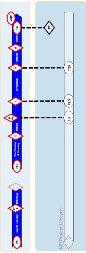
The internal APQP to NXP is called BCaM (Business Creation and Management). This method of project management was put in place in Philips Semiconductors and kept by NXP. It was based on the project management process PMI (Project Management Institute). BCaM guides project life from conception to closure (figure 2). Its objective is to enable « Doing the right projects »and « Doing the projects right » i.e. launch only those projects of strategical and financial interest, and once project acceptance granted, to lead it to success in terms of time to market, cost, quality… According to BCaM, a project can be split into different phases. Between each phase, there exist milestones for which the project needs to reach a certain level of maturity. Some criteria are defined in consultation with the customer so that when they receive the part they already know the quality level.
EiCNAM UASM32- 2015-2016 Antoine MAUDUIT
Improvement of the Volume Ramp Up Process 14
Figure 2: BCaM process : Project life cycle. => The product is officially specified at S-gate. The design of masks is then started at MRA. After the first samples are received the verification and validation starts and end at V-Gate. Between V-Gate and R-Gate the qualification is performed and the test process is prepared for production. PC stands for “Project Closure”. Once the PC gate is reached the development team is officially released and the product
EiCNAM UASM32- 2015-2016 Antoine MAUDUIT
Improvement of the Volume Ramp Up Process 15
handed over the product to Operations. The Ramp up phase officially ends at the VQD5 gate. VQD5 stands for Volume Quantity Defined 5. It corresponds to the 5% of the total quantity of units which will be produced over the life time of the product based on the business plan.
2.2 Flow of production
2.2.1 From Silicon wafers to active products
In the cycle of fabrication of a semiconductor there are several phases.
Wafer fabrication is a procedure composed of many repeated sequential processes to produce complete electrical or photonic circuits [4]. Examples include production of radio frequency (RF) amplifiers, LEDs, optical computer components, and CPUs for computers. Wafer fabrication is used to build components with the necessary electrical structures.
The main process begins with electrical engineers designing the circuit, defining its functions, and specifying the required signals, inputs, outputs and voltages. These electrical circuit specifications are fed into electrical circuit design software, such as SPICE, and then imported into circuit layout programs similar to those used for computer-aided design. It is necessary for the layers to be defined for photomask production. The resolution of circuits increases rapidly with each step in design: even at the outset of the design process the scale of the circuits is already measured in fractions of micrometres. Each step thus increases the number of circuits per square millimetre.
The silicon wafers start out blank and pure. The circuits are built up in layers in clean rooms. First, photoresist patterns are photo-masked in micrometric detail onto the wafer surfaces. The wafers are then exposed to short-wavelength ultraviolet light (λ=300 nm) and the unexposed areas are thus etched away and cleaned. Hot chemical vapours are deposited on to the desired zones and baked at high temperature (T=900°C), so as to permeate the vapours into the desired zones. In some cases, ions such as O+ or O2+ are implanted in
EiCNAM UASM32- 2015-2016 Antoine MAUDUIT
Improvement of the Volume Ramp Up Process 16
These steps are often repeated many hundreds of times, depending on the complexity of the desired circuit and its connections. The clean room air quality is highly controlled as each particle is a source of contamination (refer to table 2)
Every year there emerge new processes to accomplish each of these steps with better resolution and in improved ways, with the result that technology in the wafer fabrication industry is forever changing. New technologies result in denser packing of minute surface features such as transistors and micro-electro-mechanical systems (MEMS). This increased density continues the trend often cited as Moore's Law. [4]
Table 2: According to the norm ISO 14644-1 these are the standards for the cleanrooms in terms of particles. Maximum number ofparticles/m3
A “FAB” is a common term for the entity in which these processes are accomplished. Often the FAB is owned by the company that sells the chips, such as AMD, Intel, Texas Instruments, or Freescale. A foundry is a FAB at which semiconductor chips or wafers are fabricated to order for third party companies that sell the chip, such as FAB owned by the Taiwan Semiconductor Manufacturing Company (TSMC), United Microelectronics Corporation (UMC) and the Semiconductor Manufacturing International Corporation
EiCNAM UASM32- 2015-2016 Antoine MAUDUIT
Improvement of the Volume Ramp Up Process 17
Figure 3: In the FAB, the silicon wafer is submitted to a series of treatments (chemical, ionization, and etching) in different process steps. Different layers are created by superposing masks. These layers form passive and active components composing the product die.
Figure 4: Picture of an engineer holding a 12 inch (30 cm) diameter wafer. He is wearing an integral suit to prevent spreading potential sources of particles
The wafer test is not performed in the FAB. To control the wafers, patterns commonly called PCM are etched along the saw lines. They consist of a set of capacitors, resistances, inductors, transistors which enable the FAB to have a preview of how centred the process is with regards to control limits. PCMs are probed in the FAB before being shipped for wafer
EiCNAM UASM32- 2015-2016 Antoine MAUDUIT
Improvement of the Volume Ramp Up Process 18
test. The check-up remains basic but potentially it helps the FAB to determine the drift of a parameter such as gate oxide, poly resistor, transistor speed etc.
Wafers are shipped from the FAB to the manufacturing centre where they undergo a series of tests and transformations to become a chip shippable to the customer. The first step is the wafer test.
2.2.2 The wafer test
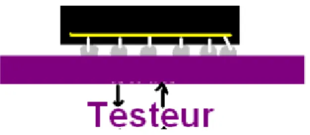
Each die of the wafer is probed. A probe card makes the interface between the tester and the die using needles in contact with the die to carry electrical signals as symbolized in figure 5. The test coverage at wafer test is only partial. A first reason for this is a technological limitation. Needles in contact with the die under test cannot deliver high frequency or high power signals.
Another reason why the coverage is low is related to the efficiency: the wider the test coverage, the longer the test time. In wafer test, the test of one die should take less than two seconds. In addition to representing a first screen stage, the wafer test is an important source of information for the FAB to identify area on the wafer showing potential sensitivity area. Based on the data feedback, the FAB can trace back tools used and fine tune certain process steps. The goal of the wafer test remains to optimize final test yield in a minimum of time. Indeed, the assembly process is expensive. Yield losses in wafer test are “cheaper” than in final test.
Figure 5: Each die is probed and is tested on wafer. Only good dies are assembled in package.
EiCNAM UASM32- 2015-2016 Antoine MAUDUIT
Improvement of the Volume Ramp Up Process 19
2.2.3 The assembly
Wafers are sawn along the saw lines (80 µm) and dies singled out as symbolized in figure 6. Based on wafer test results, good dies from wafer test will be assembled as a chip. Dies are pasted onto a lead frame. A wire bonding makes the electrical link between the die and the lead frame. The whole structure is covered by a moulding compound as a protection.
The complex process will not be detailed here. The important point to bear in mind is that the assembly yield is greater than 99.50% and the lead time roughly ten days. The assembly process reaches its maturity level very quickly in the product life span. Tin actual fact it reuses alread released technologies. During a ramp up phase, the assembly process represents only a low source of risk in terms of impact.
Figure 6: The wafers are sawn and good dies put into package for final test.
2.2.4 The final test.
Once assembled the finished product is submitted to the final test stage. The final test setup is inserted into a socket making the contact between tester resources and the unit under test as seen in figure 7. The test coverage is then exhaustive. The final test is the last control step before delivery to the customer. At this level, the unit will have to be controlled with the final goal being that is conform to the specification guaranteed to the customer. Good parts are then conditioned and packed. To give an idea, the test time per unit is roughly thirty seconds for the application type of the product line for which I am responsible.
EiCNAM UASM32- 2015-2016 Antoine MAUDUIT
Improvement of the Volume Ramp Up Process 20
If on the one hand the quality of the product is non-negociable, on the other hand excessive quality is a source of invalid yield losses. This optimization of the margin between acceptable quality and too high quality is one key element. The effort to distinguish between a valid reject and an invalid reject requires a lot of resources. And basically, optimizing one test limit once the product is released in production requires far greater effort of elaboration than making it before the product is released. The reason for this is that widening acceptance should not have any impact on the quality of the product, which is hard to prove. This fact was already mentioned earlier and it will be developed further later on. The main point is that effort has to be invested upstream.
Figure 7: Assembled products are tested in a way they are compliant with the datasheet. Yields in final test are generally greater than 95%.
EiCNAM UASM32- 2015-2016 Antoine MAUDUIT
Improvement of the Volume Ramp Up Process 21
Figure 8: Manufacturing flow. Three months are necessary to obtain the wafers from the FAB. For the wafer test, the production line needs two weeks to perform all operations. Roughly ten days are needed to assemble parts and roughly one week to perform all steps at final test.
FAB
Wafer test
Assembly
Final test
Outgoing Visual inspection
Packing
Shipping
Acceptance test
EiCNAM UASM32- 2015-2016 Antoine MAUDUIT
Improvement of the Volume Ramp Up Process 22
Before starting to quantify how large the problem is, let us define how indicators are defined and how Key Performances Indicators are settled.
3. Problem definition and definition of CTQ’s
3.1 Yield-to-area calculations (d0)
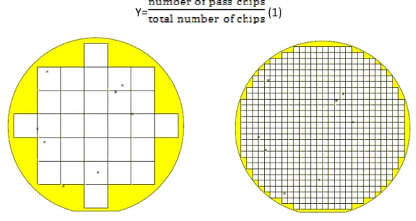
A Chessboard Test Structure (CTS) provides a list of defect positions. Based on a known wafermap each chip can be marked as "pass" or "fail" depending on the absolute position of a defect. [5] A chip is marked as "fail", if at least one defect is detected inside the chip boundaries. For a specific wafermap a yield value Y can be calculated using the following equation (1):
Y= (1)
Figure 9: Wafermap containing 29 chips. Figure 10: Wafermap containing 648 chips.
By generating a wafermap based on a given chip area A and projecting it on the original wafer, one can again calculate a yield value using the same defect list given by the data of the CTS. Figures 9 and 10 show two different imaginary wafermaps. In each wafermap, black symbols mark the defects detected inside the Chessboard Test Structures.
EiCNAM UASM32- 2015-2016 Antoine MAUDUIT
Improvement of the Volume Ramp Up Process 23
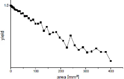
For a series of imaginary wafermaps, the yield will be determined dependent on the chip area. This results in a Yield-to-Area Curve as can be seen in the following figure 11.
Figure 11: Illustration of a Yield-to-area curve of electrically detected defects on a wafer.
Based on a given imaginary chip area A a defect density value D can be calculated using the following equation:
D= Equation 2
Where Y represents the yield, A the area of a single imaginary chip and D the defect density. This equation assumes that the wafer area is completely covered by defect sensitive test structures. However, if test structures are combined with product chips or placed inside the sawing lines, they cover just a fraction of the complete wafer area. This fact needs to be taken into account in the calculation of the defect density. We now generate four different hypothetical wafer maps as can be seen in the following Figure 12.
EiCNAM UASM32- 2015-2016 Antoine MAUDUIT
Improvement of the Volume Ramp Up Process 24
Figure 12: Here are four wafermaps with four different dies size. This is to illustrate that with a given density of defect, the yield loss is different. The bigger the die, the higher is the impact on the yield.
Based on these wafermaps, equation 2 results in the following four identical defect density values of D=0,0625 (unitless)
• (a) 256 chips with a chip area of 0.5 cm² • (b) 64 chips with a chip area of 1.0 cm² • (c) 16 chips with a chip area of 2.0 cm² • (d) 4 chips with a chip area of 4.0 cm²
This illustrates the impact of the D0 on the yield based on the area of the die. The smaller the area, the better the yield for a given D0
This illustration with its series of examples remains purely theoretical. Practically speaking, the D0 model will differ depending on :
the technology type (CMOS process, ABCD process, RF CMOS process, etc…), the technology size (140 nm, 75 nm… corresponding to the oxide thickness), the memory block proportion into the product,
conventions inside the FAB,
EiCNAM UASM32- 2015-2016 Antoine MAUDUIT
Improvement of the Volume Ramp Up Process 25
Based on the observed performances and existing models, the D0 model is adapted.
Figure 13: Impact of the memory percentage on the D0. The higher the memory percentage, the higher is the default density per mask layer.
The yield definition (Y) then matches the theoretical illustration given in the introduction to this section.
Y=0.985*EXP(-Area * D0) Equation #3
where
D0 = ((G x T) + C) x S X L. Equation #4
To define its value, the D0 is indeed composed of several variables defined by the FAB to define it value such as the Model Gradient (G), the Total Memory percentage (T) , Model Constant (C) and the number of layers (L)
The values of these parameters for our current process (CMOS14) are given in table 3: Table 3 : list of variables used for the D0 of the CMOS14
G 0.0087 C 0.00546 S 1.45 L 36
When they are inserted into the equation 2, we obtain Y (KL)= 0.985*EXP (-11.7/100*0.34)=94.6%
EiCNAM UASM32- 2015-2016 Antoine MAUDUIT
Improvement of the Volume Ramp Up Process 26
This yield is the target yield based on the FAB model. It corresponds to the theoretical yield the wafer test is supposed to reach to be in line with existing models for a given FAB process. This target yield is not necessarily in line with that defined during the business plan.
When a new defined product is accepted to go into development a profitability threshold is defined for a matrix of parameters such as
- the development budget (several tens of millions of Euros)
- a production plan for the next five years (volume in millions of units per year) - the sale price
- a test time (will impact the machine usage and hence the test cost – roughly 20 s per tested product in final test stage)
- the area of the die (the larger the die, the more wafer silicon used – ~10 mm2)
- the material used for assembly (copper or gold wire) and the production yields target.
The production yield target is there to fix a limit that ensures the margin defined at the specification phase of the product is reached.
This yield is not necessarily aligned with the one defined with the D0. A frequent explanation for this is that during the feasibility assessment, the design of the product is made in such a way that the product might lie one the edge of the process capability, which will induce yield losses. These predicted yield losses are taken into account in the business plan, so the yield is expected to be lower than the baseline. The consequence is that there might be a gap between the yield target based on the D0 and the one from the business plan.
The yield target based on the D0 remains the initial engineering target yield once production has begun. However, it might turn out to be more worthwhile to stop yield improvement activities if the yield has already reached the financial target yield laid down in the business plan. Indeed yield improvement activities are expensive in terms of resources and materials. So before one invests in yield improvement activities, a solid business case has to be defined, especially if the financial target has already been reached.
EiCNAM UASM32- 2015-2016 Antoine MAUDUIT
Improvement of the Volume Ramp Up Process 27
3.2 Type of rejects
The term “yield improvement activity” refers most of the time to the wafer test yield. This yield reflects the FAB process performance. Although the wafer test is carried out in another plant, the FAB uses wafer test yield performances to monitor its own performance. To discuss this matter in greater depth, it is now important for us to distinguish between two types of rejects: functional and parametric.
Functional rejects are those rejects that by definition are not functional. A block inside the product does not respond correctly. For instance for a failing digital block, the response signal is “0” when a “1” is expected. For an analogue signal usually characterized by a normal distribution [11], the response of a functional reject will then be an outlier as symbolized in figure 14.
By contrast, parametric rejects are those rejects that remain functional but lie beyond specification limits. The term “marginal rejects” is another commonly used name for them. This only concerns analogue signal. This type of reject is more sensitive to any variation of processes such as FAB processes or test processes. Fine tuning these processes or test limits represents the main way of yield optimization.
Figure 14:Distinction between an outlier reject and a marginal reject. Marginal rejects are sensitive to the variation of processes (test process repeatability and reproducibility, FAB process). They are contestable and are the usual targets for yield improvement activities by improving the stability of the test parameter or by re-centring the FAB process
Upper Test lim
Non-marginal reject = outliers Marginal reject
EiCNAM UASM32- 2015-2016 Antoine MAUDUIT
Improvement of the Volume Ramp Up Process 28
3.3 Representativity of distribution
The central limit theorem states that if one has a population with mean μ and standard deviation σ and one takes sufficiently large random samples from it, the distribution of the sample means will be approximately normally distributed. This will hold true regardless of whether the source population is normal or skewed, provided the sample size is sufficiently large (usually n > 30). If the population is normal, then the theorem holds true even for samples smaller than 30. In fact, this also holds true even if the population is binomial, provided that min(np, n(1-p))> 5, where n is the sample size and p is the probability of success in the population. This means that we can use the normal probability model to quantify uncertainty when making inferences about a population mean based on the sample mean.
For the random samples taken from the population, one can compute the mean of the sample means:
Equation #5
and the standard deviation of the sample means:
Equation #6
Before illustrating the use of the Central Limit Theorem (CLT) we shall first illustrate the result. In order for the result of the CLT to hold, the sample must be sufficiently large (n > 30). Again, there are two exceptions to this. If the population is normal, then the result holds for samples of any size (i.e. the sampling distribution of the sample means will be approximately normal even for samples of size less than 30).
EiCNAM UASM32- 2015-2016 Antoine MAUDUIT
Improvement of the Volume Ramp Up Process 29
The figure 15 below illustrates a normally distributed characteristic, X, in a population in which the population mean is 75 with a standard deviation of 8. On the Y-axis, is the frequency of appearances.
Figure #15 : Histogram representing a normal distribution
If we take simple random samples of size n=10 from the population and compute the mean for each of the samples, the distribution of sample means should be approximately normal according to the Central Limit Theorem. Note that although the sample size (n=10) is less than 30, the source population is normally distributed, so this is not a problem. The distribution of the sample means is illustrated below in the figure 16.
Figure #16 : Histogram representing the distribution composed of mean values
The mean of the sample means is 75 and its standard deviation sigmabar 2.5, with the standard deviation of the sample means computed as follows using the equation 6:
EiCNAM UASM32- 2015-2016 Antoine MAUDUIT
Improvement of the Volume Ramp Up Process 30
If we were to take samples of n=5 instead of n=10, we would get a similar distribution albeit a broader one. In fact, when we did this we obtained a sample mean of 75 and a sample standard deviation of 3.6.
3.4 Origin of rejects
Having described these two kinds of rejects, we can now define their origin and how to tackle these types of yield losses. Theoretically functional rejects reveal a severe failure i.e. that something has not been well processed. This is typically a FAB matter. The origin of parametric rejects leaves more room for interpretation. During the D0 definition, the expression “process capability” was mentioned. Depending on how the device was designed and specified, its performances will lie more or less closer to the limit of what the selected FAB process is able to provide. Going beyond the capability of the FAB process will make the product performances more sensitive to any environmental variations. It will be at the origin of parametric yield losses due to FAB process variations but mainly due to the ultra-sensitivity of the product. Whereas a product designed with a six sigma capability approach would absorb minor variations, a product at the edge of the FAB process will show parametric yield losses due to its ultra-sensitivity. During the design phase, the objective is to make a robust product for which natural modulations in the FAB have no impact, which is not always the case. One consequence of this is that the FAB has to work on fine tuning activities to compensate somehow too sensitive a product.
This sensitivity level is revealed during wafer test.
The main role of the wafer test remains the screening out of rejects. As mentioned earlier in our description of the production flow (Section 2.2.2), there are several reasons why the test coverage cannot be total:
EiCNAM UASM32- 2015-2016 Antoine MAUDUIT
Improvement of the Volume Ramp Up Process 31
- the second one is because one has to optimize the throughput time. The wider the test coverage, the longer the test takes. Beyond the financial aspect, the game is to optimize the machine usage and the lead time. Considering this is not the final stage, a compromise test time test coverage has to be decided upon.
The wafer test is performed at room temperature at which the trimming is done, at high temperature and at low temperature. This is a requirement of the automotive market. Not surprisingly, most functional rejects occur during the test carried out at room temperature as it also corresponds to the first time the wafer is tested. By contrast, parametric rejects occur mainly at high and low temperatures which represent extreme test conditions.
3.5 The final test
The final test is the one performed after the assembly of the die into a package. It is above all the last test stage before shipment to the customer. This means that, beyond this stage, the delivered product has to be fully compliant with the datasheet of the product. It does not mean however, that all the parameters of the datasheet have to be tested in the final test stage. The goal of testing products is not so much to characterize the product but rather to ensure they are compliant with the datasheet and that no reject is sent to the customer. These two statements might look similar but the nuance makes a big difference to the design of the test process. It means that each datasheet parameter is not necessarily intended to be individually tested but satisfied. For instance, if two parameters are shown to be correlated, only one of them need be measured. Alternatively, it might turn out to be easier or quicker to test a parameter by an indirect method.
If most of parameters will indeed be tested during this last test stage, some of them will be guaranteed by design. Most of the time, parameters guaranteed by design are those that are not testable. For instance, they might not be testable because the test would require too complex an algorithm which itself would then take too long to be tested. Or they might not be testable because measured signals would be too weak to be correctly interpreted by the
EiCNAM UASM32- 2015-2016 Antoine MAUDUIT
Improvement of the Volume Ramp Up Process 32
tester. For these reasons, products will not be tested for parameters guaranteed by design. Of course to allow a datasheet parameter not to be tested, one has to verify it shows naturally enough margins (six sigma) with regard the datasheet limit. To prove this, a representative sampling population (thirty units drawn from three different mother batches) will be measured on the lab bench.
Apart from tests guaranteed by design, there is another category of tests not included in final test. To cut test time costs, a test done in wafer test might not be repeated in final test. To meet conditions for such a case, two conditions are necessary:
1. The wafer test conditions should be stricter or equal to those in final test 2. The correlation of the parameter between wafer test and final test should be
sufficient to guarantee no risk of escape. Indeed, there are cases where the correlation between a test performed in wafer test and final test is not satisfactory because of external variables such as the effect of the package or the limitation on the impedance of the needles during wafer test.
Figure 17 shows an example of a test parameter with a good wafer test to final test correlation.
EiCNAM UASM32- 2015-2016 Antoine MAUDUIT
Improvement of the Volume Ramp Up Process 33
Figure 17: This distribution results from the measurement of a 1 MHz oscillator (X-axis). In dark blue is the distribution measured wafer test, in light green the same measure in FT. The offset on the mean between FT and WT is 20 kHz (2.0%). The offset is visible in the table above and on the cumulated plot. Typically, with so high a correlation [12], to optimize the throughput time, removing that test either in WT or in FT is to be considered. On the Y-axis, is the percentage of the cumulated plot.
The wafer test coverage is done in such a way that the yield in final test is greater than 99%. In theory, only rejects due to assembly failures should occur in final test. In practice there are tests not easily feasible in wafer test such as RF tests, once again due to the problems of needle impedance. There are technologies enabling RF tests in wafer test but they never reach performances met in final test. Performances would be sufficient to measure RF gain, output power but not to quantify parameters like RSSI. As the RF coverage is never total,
Cumulative plot
EiCNAM UASM32- 2015-2016 Antoine MAUDUIT
Improvement of the Volume Ramp Up Process 34
most of the time the choice is taken not to perform RF tests in wafer test. Making the choice not to have RF tests in wafer tests enables one
• to use cheaper needle technology and cheaper tester configuration; • to have faster wafer test sequences since RF tests are time consuming • to increase the level of parallelism (number of dies tested in parallel).
For these reasons, there are tests not done in wafer tests, which leaves the possibility of having yield losses in final test.
To recover the yield, rejects are retested once. The recovery rate is a good indicator of test process maturity. The lower the rate the more stable the test process and the higher the confidence level in the quality of the test process.
3.6 Acceptance test
An acceptance test is performed before the preparation of good parts to the delivery. It consists in retesting a sampling quantity of good parts are retested. This test has two goals:
• to ensure that good parts remain so after test and have not been damaged by it • to ensure that good parts and rejects were not intermingled.
Test limits for acceptance tests are slightly wider than in final test. If for the final test a margin is taken towards specification limits to prevent a reject is accepted, for the acceptance specification limits are applied as test limits.
Of course the acceptance criterion is that all parts pass the acceptance test. An acceptance sampling scheme is a specific set of procedures which usually consists of acceptance sampling plans in which lot sizes, sample sizes, and acceptance criteria, or the amount of 100% inspection, are related. Such schemes typically contain rules for switching from one plan to another [7]. MIL-STD-105 E (1989) is an example of a sampling scheme. The sampling quantity is defined according the AQL (Acceptance Quality Limit) 4%. Given production batches are smaller than 10,000 units, this quantity is set to 315. Similarly to the retest recovery rate during final test which is a good indicator of the health of the test process, the acceptance test is also a good indicator : for instance if five runs are required to obtain 100% passing parts, some tests must be unstable.
EiCNAM UASM32- 2015-2016 Antoine MAUDUIT
Improvement of the Volume Ramp Up Process 35
3.7 Definition of test limits based on specification limits
Tests limits are defined in such a way that delivered samples are compliant with the product specification. Delivered samples have to be compliant to the product specification not only upon delivery of the products but also after several years in service.
3.7.1 Adapting test limits to include the aging of parts
If a drift is observed during the qualification phase and accelerated aging, then test limits have to be tightened to anticipate the drift over the years. Let us consider the example in which a distribution drifted after aging from A to B. For this parameter the upper test limit will be lessened by ∆ to anticipate the drift over years as illustrated in figure 18.
Figure 18: Illustration of a drift after life test (e.g. a consumption). If after a life test a drift has been observed (∆), the upper test limit is tightened so parts remain compliant to the specification after years of usage.
3.7.2 Adapting test limits to include the repeatability of the test
Other parameters have to be incorporated in the calculation of the limit. The stability of the measurement is one of them. Each measure has its repeatability, its standard deviation. This means that if the measurement is repeated its result will vary. There are several parameters that influence the repeatability of a measurement. This one is mainly an interaction between the strength of the signal, the sensitivity of the tester, and the tester environment. Applying an averaging improve the repeatability but also increases the test time. In other words, instability is critical for the reason that it might allow through a reject as shown in figure 19.
A B
∆
EiCNAM UASM32- 2015-2016 Antoine MAUDUIT
Improvement of the Volume Ramp Up Process 36
Figure 19: Distribution of a test parameter obtained from a repeated measurement on a single sample. The distribution is so close to the upper limit that from one run to another, the reading either passes or fails.
If a measurement is repeated, the overall results form a normal distribution. This graph in figure 19 is the distribution of a test parameter repeated in loop. The area shaded in green corresponds to the left side with regard to the upper limit. It then corresponds to the area in which results pass. In this example the measurement is repeated and it happens the result passes (dark area) but in most cases it will fail. In production, the measurement is performed only once. In cases such as the one given as an example, it may happen statistically that a single measurement result falls in the dark area. Intrinsically this test parameter fails so the product has to be rejected. But due to the repeatability of the test in that example it might pass. To prevent a sample from being delivered with the risk of a failing test parameter, the repeatability has to be taken into consideration. Therefore a margin on test limits will be adapted to prevent the risk any bad elements are let through. Typically, in our example, the upper test limit will be tightened by the value of the standard deviation.
3.7.3 Tester-to-tester variation
A testing machine has its own specification provided by the manufacturer of the tester. This includes the noise floor, the sensitivity, the stability and more generally speaking its capability. It also states the maximum difference observable between testers. Indeed, despite tester machines being calibrated using the same reference checker, the uncertainty
Std dev
EiCNAM UASM32- 2015-2016 Antoine MAUDUIT
Improvement of the Volume Ramp Up Process 37
gives rise to a permanent that an offset remains. The maximum offset between testers is given in the specification of the machine. In a similar way the instability of the measurement might make a failing test parameter pass, an offset between testers might also make components with failing parameters pass.
Let us consider a parameter tested in a laboratory. In the example below, the result of the measurement fails in laboratory (L), on tester (B) but passes on tester (A). The difference between tester A and B symbolizes the reproducibility between testers as seen in figure 20.
With tester A there is a risk of over acceptance, potentially causing customer returns. With tester B there is a risk of over screening, leading to invalid yield losses with regard to the real value tester in laboratory.
Figure 20: Parameter tested on three different benches. This risk of over-acceptance has to be prevented by tightening again the limit in order to include the reproducibility between testers.
The figure 21 sums up all the parameters which are taken into consideration to compute test limits with regard to specification limits.
Result measured with tester A Result in the Laboratory Result measured with tester B
EiCNAM UASM32- 2015-2016 Antoine MAUDUIT
Improvement of the Volume Ramp Up Process 38
Figure 21: Ensemble of all the variables to be considered when computing test limits. To define test limits with regard to specification limits so there is no risk of any rejects reaching the customer as well as to prevent marginal parts drifting and failing over life time, test limits are tightened by the value of the test repeatability (for instance A), the tester-to-tester reproducibility (for instance B) and the drift over life time (C).
3.8 Hold lots criteria.
At each of these CTQ there are acceptance criteria. If any one of them is not satisfied, the production batch is put on hold for analysis.
• During wafer processing, inline monitoring guarantees that every process step lies within control limits.
• PCM must lie within control limits (generally within three sigma) before the wafer is allowed to leave the FAB.
• There are also visual inspections to check for any discoloration or scratches on the die.
• During wafer test and final test there are acceptance limits not only on the global yield but also on critical individual test parameters.
• During the assembly process there is an inline monitoring and acceptance criterion. • And naturally during acceptance tests, the last test step before delivery, all retested
good parts have to pass.
A B C C B A
EiCNAM UASM32- 2015-2016 Antoine MAUDUIT
Improvement of the Volume Ramp Up Process 39
3.9 Impacts of CTQs and criticality during volume
ramp up phase.
Naturally, production yields have a financial impact. The lower the yield the more material is needed to satisfy demand. In extreme cases, if yields are too poor the production batch might end up being scrapped. This is of course a non-negligible aspect but during a ramp up phase the priority is more delivery on time than the profitability. In addition, for low volumes, the financial consequences of having a low production yield remain acceptable.
The biggest impact of production yields during the ramp up phase is on the lead time. The poorer the yield the more material is required. This means that every process will lose in efficiency so to compensate low production yields more material has to be manufactured and tested. Here lies the main impact on the lead time. Especially during the ramp up phase there is no slack in the warehouse. An unpredictable lead time is a source of delay.
Another impact of having low yield is a risk of raw material shortage, the lead time or obtaining new wafers being roughly two months. Between the time the product is officially released and the time enough wafers are in the wafer bank to cover frequent manufacturing incidents, it can take months. During this period, having low production yield weakens delivery capability. A side effect of having low production yields is also that the quality level is at risk. Indeed, if for instance 50% or 60% of units in a sample batch fail, there must be something wrong with either the tester material or the test environment. Even if good parts of that batch passed the test sequence, the confidence level regarding the quality level is questionable.
EiCNAM UASM32- 2015-2016 Antoine MAUDUIT
Improvement of the Volume Ramp Up Process 40
Figure 22: This figure gives the list of “Critical To Quality” factors, parameter contributing to them and how they interfere with each other. The production yield remains the biggest contributor. The yield coupled to the cycle time are the major contributor to the throughput time (TPT). The open/short rate (O/S) corresponds to the percentage of samples not functional at all. BR@T is the name of the system managing hold lot criteria
Low yields are mainly due to the fact that the test process and the manufacturing processes are not yet mature. Encountering low yields and going over the learning phase which is a cause of incidents increases the risk of hold lots at every process step. This slows down the throughput time. Figure 22 gives an illustration of how parameters impacting the manufacturing processes are cascaded leading to throughput time slow down. The length of this learning period will depend on the degree of innovation embedded into the new product.
The challenges faced during the volume ramp up are thus to provide delivery on time and with the correct quality level.
EiCNAM UASM32- 2015-2016 Antoine MAUDUIT
Improvement of the Volume Ramp Up Process 41
4. Quantification of the problem
4.1 Impact on yield performances
The problem which has been addressed by this study is to minimize the impact linked to the volume ramp up phase and secure the early deliveries: The aim is to make production yields and lead times stable and on target as soon as possible during the ramp up phase so as not to risk delivery shortage and customer returns. Before discussing the approach adopted to find solutions, let us first discuss the severity of the problem.
As an illustration let us consider just the production yields and hold lot rates of a few products released into production in 2010-2011 Here are yield figures for a high runner released in 2011 as shown in figure 23 and 24.
Figure 23: Product yield of one of our high runner products over a two year period. Each data represents the yield reached by production batches. To make our discussion more concrete, let us suppose that one production batch in final test is composed of roughly 4000 units which somehow matches with the quantity of the reel shipped to the customer. To make the graph easier to read, the scale was cut off at 90% although there were occurrences below the minimum shown on the graph.
The hold lot limit is symbolized by the thick line. If the yield of a production batch falls below 96% it will be put on hold and will require an analysis before being released. If the case is
EiCNAM UASM32- 2015-2016 Antoine MAUDUIT
Improvement of the Volume Ramp Up Process 42
known, the batch will be released in one or two days. If it is a new case, it might take several days to be released, which might lead to a rescreening of good parts. This has an impact on the throughput time. As a side effect, it has an impact on the workload on the engineering team.
What we also observe is the trend line increasing over the time thanks to yield improvement activities. The approach making a yield improvement will be detailed later. Basically, yield improvement activities are led to tackle invalid rejects. This is mainly to minimize the need to invest in yield improvement activities once the product is in production that the project has been led.
Figure 24: This graph displays data of Figure #23 this time in histogram form [10]. It helps one to figure out the frequency of occurrences.
EiCNAM UASM32- 2015-2016 Antoine MAUDUIT
Improvement of the Volume Ramp Up Process 43
Figure 25: Percentage of hold lots with regard to the number of tested batches. If the production well started in January 2013, the hold lot rate increased drastically in May leading to a crisis period. It took almost one year for the hold lot rate to be brought back to an acceptable level.