HAL Id: hal-00629297
https://hal.archives-ouvertes.fr/hal-00629297
Submitted on 5 Oct 2011
HAL is a multi-disciplinary open access
archive for the deposit and dissemination of
sci-entific research documents, whether they are
pub-lished or not. The documents may come from
teaching and research institutions in France or
abroad, or from public or private research centers.
L’archive ouverte pluridisciplinaire HAL, est
destinée au dépôt et à la diffusion de documents
scientifiques de niveau recherche, publiés ou non,
émanant des établissements d’enseignement et de
recherche français ou étrangers, des laboratoires
publics ou privés.
Threshold Operation
Mariem Slimani, Fernando Silveira, Philippe Matherat
To cite this version:
Mariem Slimani, Fernando Silveira, Philippe Matherat. Variability-Speed-Consumption Trade-off in
Near Threshold Operation. PATMOS 2011, Sep 2011, Madrid, Spain. pp.308–316,
�10.1007/978-3-642-24154-3_31�. �hal-00629297�
Variability-Speed-Consumption Trade-off in
Near Threshold Operation
Mariem Slimani1, Fernando Silveira2, and Philippe Matherat1
1 Institut TELECOM, TELECOM-ParisTech, LTCI-CNRS
46, rue Barrault, 75634 - Paris Cedex 13, France, slimani.mariem, [email protected]
2 Universidad de la Rep´ublica, Instituto de Ingenier´ıa El´ectrica,
J. Herrera y Reissig 565, 11300 Montevideo, Uruguay, [email protected]
Abstract. Sub-threshold operation is an efficient solution for ultra low
power applications. However, it is very sensitive to process variability which can impact the robustness and effective performance of the cir-cuit. On the other hand this sensitivity decreases as we move towards near-threshold operation.
In this paper, the impact of variability on sub-threshold and near-threshold circuit performance is investigated through analytical modeling and cir-cuit simulation in a 65 nm industrial low power CMOS process. We show that variability moves the effective minimum energy point towards the near threshold region. Thus, we demonstrate that when variability is taken into account, a complete model that includes the near threshold (moderate inversion) region is necessary in order to correctly model cir-cuit performance around the minimum energy point. Finally, we present the resulting speed-consumption trade-off in a variability-aware analysis of sub-threshold and near-threshold operation.
Keywords: Sub-threshold logic; Near-threshold operation; Variability;
Modeling
1
Introduction
Over the last decade, sub-threshold logic has been used as an ideal option to achieve Ultra Low Energy consumption for applications with low demand in speed requirements. Here, sub-threshold term refers to the weak inversion (WI) region where the minimum energy can be achieved using a supply voltage VDD
well below the threshold voltage.
As the interest for ultra low energy has increased, research related to sub-threshold logic has attained considerable importance. Modeling and character-ization of sub-threshold operation for standard CMOS cell designs have been investigated for energy and performance analysis[1][2].
However, several works have shown that variability in subthreshold logic, espe-cially intrinsic one due to Random Dopant Fluctuations (RDF), is a critical limit
to achieve robust ultra low energy devices as it cannot be compensated through adaptive body biasing (ABB)[3][4][5]. As currents in weak inversion region expo-nentially depends on threshold voltage (Vt), random Vt variations significantly
affect the on and off currents and gate delays and can affect the output swings and result in functional failures of some gates. Moreover, the minimum energy point can be strongly affected by variability. As reported in [6], device variability leads to 20% of minimum energy increase.
Models considering variability have been developed in previous works specif-ically for use in subthreshold, considering, therefore, just the weak inversion region. In this paper, we will show through 1K-point Monte Carlo Spice simula-tions in a Low Power (LP) technology from an industrial foundry that variabil-ity moves the effective minimum energy point towards the near-threshold region (Moderate Inversion). Thus, restrictive weak inversion models can no longer model circuit performance around the minimum energy point.
Therefore, we apply a complete and compact transistor model valid from weak to strong inversion in order to model the delay and energy performance over the weak and moderate inversion regions. This will allow us to correctly model the circuit performance in a variability aware analysis.
This paper is organized as follows. Section 2 presents the concept of sub-threshold operation and investigates the impact of process variations on mini-mum energy point. In section 3, we propose a complete model that includes the near threshold region. We show through Monte Carlo Spice simulations that the new model is necessary to correctly model the circuit performance in a variability aware analysis.
2
Sub-threshold circuit design
In this section, the concept of sub-threshold operation is briefly explained. Vari-ability impact on sub-threshold circuit performance through Monte Carlo Spice simulations of an inverter chain implemented in a Low Power technology from an industrial foundry is then presented.
2.1 Sub-threshold operation
Sub-threshold operation consist in reducing the power supply voltage VDDbelow
the threshold voltage VT in order to achieve minimum energy consumption. The
concept is simple: as Pdynis proportional to the square of VDD, a small reduction
in supply voltage causes quadratic decrease in dynamic power consumption at the cost of a significant increase in delay. This results in an increase in leakage energy that leads to a minimum energy point achieved at an optimum supply voltage. In[7], authors provide an analytical solution for the optimum VDD that
minimize the energy for a given operating frequency.
However, lowering the power supply voltage will expose the circuit to the effect of process variations which can impact the functionality of the circuit and result in a functional failure of the gate. Thus, a process corners analysis
Variability-Speed-Consumption Trade-off in Near Threshold Operation 3
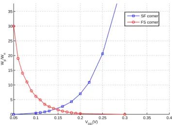
which determines the minimum operation voltage and the minimum transistor sizing which ensures a good functionality of the gate is the first step to do, as described in [2]. We have applied this analysis to an inverter from a 65nm Low Power industrial library. Figure 1 shows the limits for the ratio of the pMOS width to nMOS width, which must be between the minimum set by the Fast 0-Slow 1 (FS) corner and the maximum set by the Slow 0-Fast 1 (SF) corner in order to assure an output swing of 10%-90% of the supply voltage.
0.050 0.1 0.15 0.2 0.25 0.3 0.35 0.4 5 10 15 20 25 30 35 VDD(V) Wp /W n SF corner FS corner
Fig. 1.Worst case corners analysis of the inverter for different supply voltage.
We observe that this restriction determines a minimum possible operating voltage, which for this technology occurs at 143mV by sizing the PMOS width to be 1.83 the NMOS one. We see that the inverter of the standard cell library is guaranteed to operate down to 160mV. Thus, if the minimum energy point is achieved by a supply voltage between 143mV and 160mV, a modified logic cell library should be created.
2.2 Variability effect on subthreshold circuit
Process variations is a critical limit of sub-threshold circuits. Intrinsic variations due to Random doping fluctuation (RDF) is considered to be the dominant source of variability in sub-threshold circuits [5].
To show the impact of variability on sub-threshold circuit performance, Monte Carlo Spice simulations with 1000 points have been performed for different val-ues of VDD. The considered benchmark circuit is a chain of inverters where the
first inverters are not considered in order to correctly calculate the static cur-rent, increased due to the degeneration of stable states as mentioned in [1]. Since
delay variability depends on the logic depth of the circuit, an appropriate choice of the logic depth is essential. For our case study, we have choosen a logic depth of 23 like in [8] where the circuit is a standard 8-bit ripple-carry-array (RCA) multiplier.
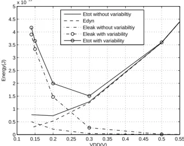
Figure 2 shows the evolution of total energy consumption without and with variability effect, considering typical and 3σ worst case delay, respectively.
0.1 0.15 0.2 0.25 0.3 0.35 0.4 0.45 0.5 0.55 0 0.5 1 1.5 2 2.5 3 3.5 4 4.5 5x 10 −15 VDD(V) Energy(J)
Etot without variabiltiy Edyn
Eleak without variabiltiy Eleak with variability Etot with variability
Fig. 2.Leakage and total energy evolution with and without variability.
We observe that variability leads to a considerable increase in leakage energy. This results in the increase of the minimum energy point by 50%, located now in the moderate inversion region.
3
Variability aware circuit model
In[1],[5] and [6], models in WI region are applied to describe sub-threshold op-eration. However, as we have seen in section 2, variability considerably affects the minimum energy point which moves in the moderate inversion region. In[1] the impact of operation in moderate inversion applying an all region transistor model is also considered, but the impact of variability is not analyzed in this case. [9] is another prior work where authors suggest to work in the near thresh-old voltage region in order to recover some of delay performance at the expense of a little energy increase. An energy-delay modeling framework that extends over all inversion regions is developed in this paper. But variability is still not considered in these models.
Variability-Speed-Consumption Trade-off in Near Threshold Operation 5
In this section, we present a variability aware model that extends over the weak and moderate inversion region. This model is based on the EKV model expressions [1]. The main contribution here is that we consider VT and β
varia-tions in our analysis. We show through Spectre and Matlab simulavaria-tions that the WI model in no longer sufficient to model the performance of a system exposed to process variations.
3.1 Current and delay model under variability analysis
In weak and moderate inversion region, the drain current can be expressed as[1]:
IDS =IS(ln2[1 + exp VGS− VT 2nUT ]− ln2[1 + expVGS− VT 2nUT exp −VDS 2UT ]) (1)
Where n is the subthreshold slope factor, VGS and VDS are respectively the
gate to source and drain to source voltages and VT is the threshold voltage. IS
is the specific current given by
IS = 2nµCoxUT2W/L = 2nβUT2 (2)
Where µ is the mobility, Cox is the oxide capacitance, UT is the thermal
voltage and W/L denotes the channel width-length ratio of the transistor. Equation 1 tends to the classical exponential WI model when VGS− VT is
neg-ative.
The expression of delay can be derived from the current model as follows:
Td=
CLVDD
Ion
(3)
Where CL is the load capacitance, VDD is the supply voltage and Ion is the
saturated on-current.
Leakage current is also determined from the IDS expression when VGS= 0.
The model of Equation 1 is a long channel model that does not include effects such as mobility reduction, velocity saturation and drain induced barrier lowering (DIBL). The former two are mainly of impact in the strong inversion region and that is why, for simplicity sake, were not considered in this work. The last one (DIBL), has some impact on the performance in the WI and MI regions, as analyzed in [5]. In our case we considered the effect of DIBL when extracting the parameters for the model of Equation 1 by considering the drain current data of the 65nm Standard Threshold Voltage, Low Power (SVTLP) NMOS transistor with drain voltage equal to VG. To extract model parameters, we have
applied the method based on the gm/ID curve described in [10]. The following values were obtained:
– n = 1.22; – VT = 0.38(V);
– β = 4.83e−4(A/V2).
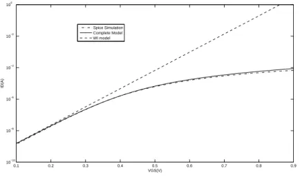
Figure 3 shows the IDversus VGSfor NMOS transistor determined with the
weak inversion model, the complete model and spice simulations. As expected, the weak inversion model is not sufficient to model the current in near-threshold region. We observe that the complete model is not so accurate in strong in-version region due to the lack of modeling of mobility reduction and velocity saturation[10]. 0.1 0.2 0.3 0.4 0.5 0.6 0.7 0.8 0.9 10−10 10−8 10−6 10−4 10−2 100 VGS(V) ID(A) Spice Simulation Complete Model WI model
Fig. 3. ID versus VGS curves for NMOS transistor.
For variability analysis, we will consider just random VT and β variations,
modeled as a normal distributions (µVT, σVT, µβ, σβ), determined through Monte
Carlo simulations or through analytical expressions given in [5]. Current model considering process variations is derived from Equation 1 by replacing β and VT by values that follow the normal distribution described in the previous
para-graph.
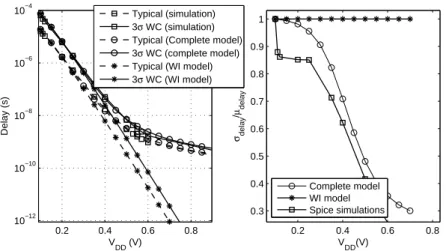
The evolution of typical and 3σ Worst Case(WC) delay is presented in Fig-ure 4 (left). We observe that the complete model with and without variability consideration follow perfectly Monte-carlo Spice simulations whereas the delay of the WI model deviates from 0.3V of Vdd.
Figure 4 (right) plots delay variability versus the supply voltage. The simu-lated variability, obtained through Monte-Carlo simulations, shows that variabil-ity decreases as the supply voltage increases. We remark that delay variabilvariabil-ity, obtained with the WI model, remains constant at different supply voltage, while, the one obtained with the complete model presents the same shape as spectre simulations and has even close values.
Variability-Speed-Consumption Trade-off in Near Threshold Operation 7 0.2 0.4 0.6 0.8 10−12 10−10 10−8 10−6 10−4 VDD (V) Delay (s) Typical (simulation) 3σ WC (simulation) Typical (Complete model) 3σ WC (complete model) Typical (WI model) 3σ WC (WI model) 0.2 0.4 0.6 0.8 0.3 0.4 0.5 0.6 0.7 0.8 0.9 1 VDD(V) σdelay / µdelay Complete model WI model Spice simulations
Fig. 4. Evolution of typical and WC delay (left), and normalized delay variability
(right) for different VDD.
We conclude that the WI model is a restrictive model that can not be used to model process variations and that the model developed, considering VT and
β variations, is a good model for variability analysis.
The delay model presented in Equation 3 is valid for a simple gate. For a circuit with a logic depth LD, the delay will be Tcircuit= LD.Td. If Tdis a normal
distribution defined by (µdelay, σdelay), Tcircuitwill be a normal distribution too
defined by (LD.µdelay,p(LD).σdelay). Thus, the delay variability of the circuit
can be obtained as follow:
varcircuit−delay= (1/p(LD)).vargate−delay (4)
Table 1 lists delay variability for different Logic depth at VDD= 0.2V .
Table 1.Delay variability for different logic depth at Vdd=0.2 V.
LD Delay variability (σdelay/µdelay)
Spice simulation Analytical model
1 0.86 0.99
7 0.28 0.36
15 0.25 0.26
23 0.205 0.209
As expected, the delay variability of a circuit decreases as its logic depth increases, and the decrease follows perfectly 1/p(LD) law.
3.2 Energy model under variability analysis
The total energy consumed by the circuit is the sum of the dynamic energy Edyn,
required to charge and discharge parasitic capacitances during logic transitions, and static energy Estat due to leakage currents Ileak. This can be summerized
in the following expression :
Etot= αCLVDD2 + VDDIleakTcircuit (5)
Where α is the switching activity of the circuit and CLis the load capacitance.
Here, we consider Just − in − time operation [11], where the circuit works in its maximum frequency, i.e., the period is set to be the critical path delay of the circuit.
To consider variability in energy analysis, 3σ worst-case delay and mean Ileak
are considered in the static energy calculation as follows Estat= VDDµIleakµdelay(1 + 3 ∗
σdelay
µdelay
) (6)
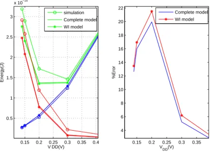
Figure 5 shows the consumed energy under process variations consideration.
0.15 0.2 0.25 0.3 0.35 0.4 0.5 1 1.5 2 2.5 3 x 10⁻¹⁵ VDD(V) Energy(J) simulation Complete model WI model 0.15 0.2 0.25 0.3 0.35 4 6 8 10 12 14 16 18 20 22 VDD(V) %Eror Complete model WI model
Fig. 5.Consumed energy under process variations (left), and % of complete and WI
model error compared to Spice simulations (right).
We observe that the total energy consumed is slightly different from that determined by the models. The error of the energy on the minimum point is of
Variability-Speed-Consumption Trade-off in Near Threshold Operation 9
5% and 6%, when obtained by the complete and the WI model, respectively. Not what we expect, the error of the WI model is comparable to that of the com-plete model as shown in Figure 5 (right). This can be explained by the inverse tendency of variability and delay determined by the WI model. On the one hand, the variability of the WI model is constant whatever the value of the supply volt-age. It is therefore overestimated in the moderate and strong inversion regions. On the other hand, the delay obtained by the WI model is underestimated with respect to the one obtained by Spice simulations as observed in Figure 4. As the energy contains the product of variability and the delay, there is a com-pensation that let the WI model remain a good model of energy consumption even under variability analysis.
4
Conclusion
In this paper, modeling under variability analysis is investigated. We show that the Weak Inversion model, normally used to describe sub-threshold circuit, is a restrictive model that can no longer model circuit delay around the minimum energy point of circuit exposed to process variations.
We develop a complete model that extends over the weak and moderate inversion regions. Through Monte Carlo Spice simulations of a chain of inverters in a Low Power technology, we show that the new model is necessary to correctly model the variability of the circuit.
Nevertheless, instead of what may be expected, the Weak Inversion model remains a good model of energy consumption even under variability analysis. This is due to the compensation of delay and variability errors resulting when the WI model is applied.
Acknowledgments.
The authors would like to thank STIC AmSud Program for the financial support given to this work through the NanoRadio project.
References
1. Vittoz, E. : Weak inversion for ultimate low-power logic: in Low-Power CMOS Cir-cuits, Ed. Christian Piguet, CRC, (2006)
2. Wang, A., Chandrakasan, A. : A 180-mV subthreshold FFT processor using a min-imum energy design methodology: Solid-State Circuits, IEEE Journal of, vol. 40, no. 1, pp. 310-319, IEEE, (2004)
3. Hanson, S., Zhai, B., Blaauw, D., Sylvester, D., Bryant, A., Wang, X. : Energy optimality and variability in subthreshold design: in Low Power Electronics and Design, 2006. ISLPED’06. Proceedings of the 2006 International Symposium on IEEE, pp. 363-365, (2007)
4. Verma, N., Kwong, J., Chandrakasan, A. : Nanometer MOSFET variation in min-imum energy subthreshold circuits: Electron Devices, IEEE Transactions on, vol. 55, no. 1, pp. 163-174, (2007)
5. Bol, D., Ambroise, R., Flandre, D., Legat, J. : Interests and limitations of technology scaling for subthreshold logic: Very Large Scale Integration (VLSI) Systems, IEEE Transactions on, vol. 17, no. 10, pp. 1508-1519, (2009)
6. Bol, D., Kamel, D., Flandre, D., Legat, J. : Nanometer MOSFET effects on the minimum-energy point of 45nm subthreshold logic: in Proceedings of the 14th ACM/IEEE international symposium on Low power electronics and design, pp. 3-8, ACM, (2009)
7. Calhoun, B., Chandrakasan, A. : Characterizing and modeling minimum energy operation for subthreshold circuits: in Low Power Elec- tronics and Design, 2004. ISLPED’04. Proceedings of the 2004 International Symposium on IEEE, pp. 90-95, (2005)
8. Bol, D. : Pushing ultra-low-power digital circuits into the nanometer era: Ph.D. dissertation, University of California, (2008)
9. Markovic, D., Wang, C., Alarcon, L., Rabaey, J. : Ultralow-power design in near-threshold region: Proceedings of the IEEE, vol. 98, no. 2, pp. 237-252, IEEE, (2010) 10. Jespers, P. : The Gm/ID Methodology, a Sizing Tool for Low-voltage Analog CMOS Circuits: The Semi-empirical and Compact Model Approaches. Springer Verlag, (2009)
11. Seok, M., Hanson, S., Sylvester, D., Blaauw, D. : Analysis and optimization of sleep modes in subthreshold circuit design: in Proceedings of the 44th annual Design Automation Conference, pp. 694-699, ACM, (2007)