HAL Id: hal-01367238
https://hal-univ-rennes1.archives-ouvertes.fr/hal-01367238
Submitted on 14 Oct 2016HAL is a multi-disciplinary open access archive for the deposit and dissemination of sci-entific research documents, whether they are pub-lished or not. The documents may come from teaching and research institutions in France or abroad, or from public or private research centers.
L’archive ouverte pluridisciplinaire HAL, est destinée au dépôt et à la diffusion de documents scientifiques de niveau recherche, publiés ou non, émanant des établissements d’enseignement et de recherche français ou étrangers, des laboratoires publics ou privés.
natural graphite under electrochemical conditions
P. Poizot, B. Humbert, C.P. Ewels, J.-Y. Mevellec, N. Stephant, J. Simonet
To cite this version:
P. Poizot, B. Humbert, C.P. Ewels, J.-Y. Mevellec, N. Stephant, et al.. Facile route to gold-graphene electrodes by exfoliation of natural graphite under electrochemical conditions. Carbon, Elsevier, 2016, 107, pp.823–830. �10.1016/j.carbon.2016.06.079�. �hal-01367238�
M
ANUS
C
R
IP
T
ACCEP
TED
Facile Route to Gold-Graphene Electrodes by Exfoliation of Natural
Graphite under Electrochemical Conditions
Philippe Poizota,b,*, Bernard Humberta, Chris Ewelsa, Jean-Yves Mevelleca, Nicolas Stéphanta, Jacques Simonetc,**
a Institut des Matériaux Jean Rouxel (IMN), UMR CNRS 6502, Université de Nantes, 2 rue de la Houssinière, B.P. 32229, 44322 Nantes Cedex 3, France
b Institut Universitaire de France (IUF), 103 bd Saint-Michel, 75005 Paris cedex 05, France c Sciences Chimiques de Rennes (MaCSE), UMR CNRS 6226, Université de Rennes 1, Campus de Beaulieu, 35042 Rennes Cedex, France
Abstract
An original and practical procedure for preparing graphene-modified gold electrodes has been developed by careful control of the electrochemical exfoliation process of natural graphite. Pre-exfoliated (intercalated) graphite is first mechanically deposited onto a gold electrode. A cathodic treatment is then performed in N,N-dimethylformamide containing tetraalkylammonium salts at potential lower than -2 V vs. Ag/AgCl. This erodes the carbon coating through exfoliation of graphite particles. The result of this simple process, as identified by Raman spectroscopy, is a highly stable carbon surface made of graphene sheets, that gives well reproducible voltammetric responses (both in potential and intensity). Confocal Raman microspectrometry demonstrates that the bonded graphene phase consists of either 1 or 3 layers over micron-sized areas of the gold substrate. These layers can then subsequently be used as a trap to fix different organic groups. This easy and highly reproducible process could greatly simplify gold-graphene electrode production in the field of electrochemistry of graphite and its parent compounds.
M
ANUS
C
R
IP
T
ACCEP
TED
1. IntroductionThe development of carbonaceous electrode materials is of great of interest for numerous applications ranging from analytical purposes to electrochemical storage systems. Glassy carbon (GC) is commonly used as a convenient electrode material for electroanalysis and electrolysis within the cathodic domain [1]. However interest is growing in graphite, especially when reduced at potentials lower than -1.8 V vs. Ag/AgCl (in organic polar aprotic solvents). In these conditions it can intercalate cations with possible exfoliation [2], resulting in peculiar cathodic materials that behave as reducing species according to their electron transfer processes [3]. Interestingly, GC was also reported to be no longer inert at quite reducing potentials (< -1.7 V vs. Ag/AgCl), due to the presence of ribbons or other graphite-like structural inclusions [4,5]. Hence a key point in modification of GC electrodes is to consider this material as containing graphite-like domains, which give rise to poly-nucleophilic centres when cathodically polarized [6,7]. The cathodic charging of these C sp2 -inclusions, which is accompanied by the insertion of organic or inorganic cations, mimics many nucleophilic reactions for “reduced” GC with a large selection of possible electrophilic reagents [7].
Beyond GC and regular graphite, interest in graphene-based electrodes is also emerging due to the peculiar physical/chemical properties of this carbonaceous material. Interest in graphene has taken off since the discovery of easy methods to fabricate and characterize it [8-10]. In particular Raman spectroscopy can be considered as the characterization technique of choice, especially for understanding the behaviour of electrons and phonons in graphene. Many ingenious approaches for producing graphene sheets are known: the recent literature is abundant for instance in organic methods (total synthesis [11]) and others relying on solution-based chemical and electrochemical processes [12-16]. Notable is an original method [17] based on graphite exfoliation in ionic liquids. The common electrochemical approach to obtain graphene remains the reduction of graphene oxide [18], but the electrochemical method based on disaggregating graphite through exfoliation appears promising. Finally, electrochemistry has also been used to modify commercially available graphenes, such as 3D {graphene-GC} electrode modified with redox units for use in catalysis [19]. When using fluidized bed processes, graphene suspensions could permit large scale electrochemical functionalization. For instance, carboxylation reactions of graphene were performed at high yield, approaching one carboxylate functional group per hundred carbons [20]. In short, although there is a clear need for new methodologies for fabricating graphene-based electrodes, this remains a challenging task.
M
ANUS
C
R
IP
T
ACCEP
TED
The current contribution is inspired by the electrochemical splitting of graphitic materials via the intercalation of tetraalkylammonium (TAA+) cations under specific conditions, a method discovered by one of us almost four decades ago [2]. We demonstrate here through
a Raman study that simple graphite-based deposition onto gold followed by an electrochemical erosion process leads to Au interfaces with thin graphene coverage. The
result is a stable graphene-modified gold electrode. The building of such interfaces is particularly easy, and gives highly reproducible electrochemical responses in current and potential. This is interesting and useful for electrochemical analysis applications such as cathodic charge in the presence of different salts, and the concomitant addition of functionalised free radicals on these radicalophile materials.
2. Experimental
2.1. Procedure for preparing working electrodes
Gold disk microelectrodes (S = 0.8 mm2) used for the deposition of graphite were first carefully polished with coarse (Struers 500) and then finer (Struers 1200) silicon carbide polishing paper. Before use, natural graphite (from Ceylon) was first partly exfoliated by cathodic treatment (electrochemical intercalation of graphite). More precisely, graphite (80 mg) was submitted to a reduction process (Er = -2.1 V vs. Ag/AgCl) in 0.1 M TMABF4 using DMF as solvent and a three compartment cell (cathodic compartment: V ≈ 8 mm3, efficient stirring, electrode: mercury pool with a surface area of 5 cm2). The starting current was about 2 mA, and the graphite treatment was stopped after charge of 7 C was passed through the cell. The as-prepared intercalated graphite was then filtered from the electrolytic solution, rinsed several time with water then acetone, and finally dried for 20 min at 60°C. This pre-exfoliated graphite was finally mixed with acetone to form a slurry, which was coated on gold disk microelectrodes. Once the acetone evaporated, the electrode was firmly rubbed on a glassy cardboard in a polishing manner until the surface obtained a shiny aspect. Very short sonication may help to eliminate residual graphite flakes if any.
2.2. Electrochemical experiments
Voltammetric and coulometric measurements were performed with a PAR 273 potentiostat using three-electrode cells separated with a fritted glass. All potentials are referring to an aqueous saturated calomel electrode (SCE). The measurements were carried out in 0.1 M solutions of tetraalkylammonium salts (TAAX), primarily tetrafluoroborates
M
ANUS
C
R
IP
T
ACCEP
TED
tetrapropylammonium (TPA ), tetra-n-butylammonium (TBA ), tetra-n-hexylammonium (THA+), and tetra-n-octylammonium (TOA+) in upper grade N,N,-dimethylformamide (DMF). All the experiments described in this work did not need any special treatment of electrolytic solutions when fresh DMF solutions are employed. The water content in electrolytic solutions never exceeded 800 ppm.
2.3. SEM imaging, Raman characterizations and related statistical treatment
Scanning Electron Microscopy (SEM) analyses were performed using a JEOL JSM−7600F microscope. Raman spectra were recorded using a microconfocal Raman Invia Reflex, equipped with a double edge filter to eliminate the Rayleigh scattering, and a Charged Couple Device (CCD) camera working at a temperature of 220 K with a 1024 by 256 pixel array. Laser excitations were at 514.53 nm, 633 nm and 785 nm. The setup consists of a confocal microscope equipped with an automated XYZ table, where the displacement motors were able to generate 100 nm steps with a spatial precision better than 100 nm verified on an AFM grid. The spectral resolution achieved with the use of gratings of 2400, 1800 or 1200 grooves per millimeter was between 3 and 4 cm-1 according to the excitation wavelength. The focused power of the laser beam was also checked for each wavelength to avoid any transformation or heating of the samples. Accordingly, the power was kept below 100 μW and the magnitude ×100 of the objective has been selected after a test list. The confocal mode was also sometimes used to select a smaller analyzed volume in the same irradiated volume or to record Raman maps with better spatial resolution (around at λ/2). Samples studied in this paper were heterogeneous at the micrometer scale.
Raman spectra were decomposed using either a set of symmetric bands characterized by a fixed parameter set (position, full-width at half height, profile) or a multi-curve resolution method previously developed in our group [21-23], the Bayesian Positive Source Separation (or BPSS) curve resolution method. The BPSS method gives an estimation of the unknown component spectra and the concentrations of the underlying species. Where spectroscopic techniques fail to resolve unknown or unstable individual constituents contained in multi-component mixtures, vibrational spectroscopies combined with BPSS treatment may offer a promising and efficient approach.
3. Results and discussions
Prior to discussing gold modification by graphene, it is important to state that the optimized experimental procedure starts by a pre-exfoliation reaction of natural
M
ANUS
C
R
IP
T
ACCEP
TED
graphite by cathodic treatment in 0.1 M TMABF4 using DMF as solvent (although the
direct use of natural graphite is possible). Afterwards, this preliminarily “expanded”
graphite is deposited onto gold working electrodes (Au disks) and then reduced within a quite large range of potentials in solutions of tetraalkylammonium salts (TAAX) in DMF. For instance, Fig. 1 shows a typical cyclic voltammogram (CV) obtained with TEABF4. While a pristine polished Au disk does not show any significant signal, an intense peak appears in reduction with the modified Au disk (scan 1), which is assigned to a large charge associated with insertion of TEA+ cations between graphitic layers. This cathodic peak is then followed by an abrupt current decay corresponding to the dislocation of the graphite deposit. This electrochemical erosion process was visible by eye, as the working electrode turned from a shiny grey to a bright yellow pristine gold colour. A rough schematic of the assumed whole process occurring during the first cathodic scan is proposed in Fig. 1. Several experiments with different TAA-based salts revealed that the most efficient erosion of the carbon
coating on gold microelectrodes were obtained with TMA+ (associated with BF4- or ClO4-).
All results presented here were repeated several times with different electrodes to ensure the reproducibility of the results.
Figure 1. Electrochemical response for a thick deposit of pre-exfoliated graphite onto gold
during two consecutive cathodic scans from -0.2 to -2.2 V/SCE (electrolyte: 0.1 M TEABF4 in DMF; v = 50 mV s-1), together with a possible reaction pathway as the first cathodic sweep proceeds (see illustration) leading to a residual stable carbon deposit onto Au (after exfoliation, E < - 1.8 V /SCE).
M
ANUS
C
R
IP
T
ACCEP
TED
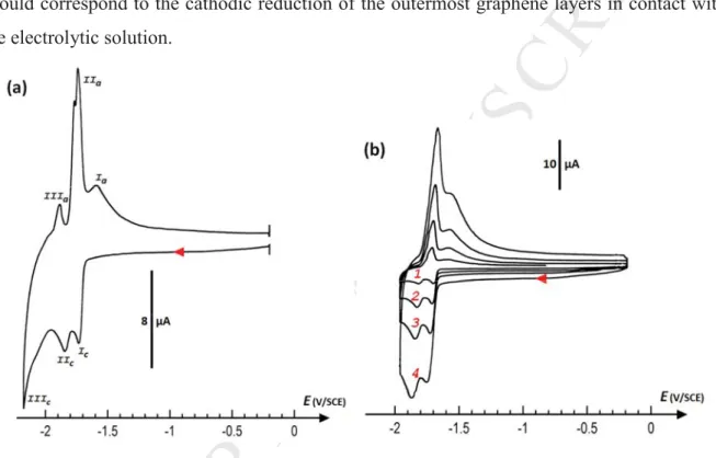
By the second cycle, quite reproducible CVs were systematically obtained and characterized by reversible faradaic peaks located from -1.5 to -2.2 V (Fig. 1, 2nd scan). At this stage, this electrochemical behaviour suggests that a thin and stable electroactive interface exists on the electrode after a first cathodic scan, possibly related to residual stacking of graphene layers on the Au substrate. Note that the shape of these recurrent CVs strongly depends on the TAA+ used. For example, three electrochemical faradaic peaks are observed when using TEA+
with both cathodic and anodic correlated contributions (Fig. 2a, peaks denoted I, II, and
III). Interestingly, these peak currents appear proportional to the scan rate (Fig. 2b), which should correspond to the cathodic reduction of the outermost graphene layers in contact with the electrolytic solution.
Figure 2. a) Focus on the resulting CV curve after a first cathodic scan for a thick deposit of
pre-exfoliation graphite onto gold (SAu(disk) = 0.8 mm2; v = 50 mV s-1; electrolyte: 0.1 M TEABF4 in DMF). b) Corresponding influence of the scan rate on the CV curves (1: 20 mV s -1; 2: 50 mV s-1; 3: 100 mV s-1; 4: 200 mV s-1). Currents of main faradaic peaks are proportional to the scan rate.
This electrochemical data suggests a TAA+ coverage of about 1.6 × 10⁻⁸ mol cm-2 based on integration of the cathodic wave from -1.5 to -1.7 V. While this value appears quite
large, we should take into account an expected highly disturbed geometry of the graphene-gold interface. Other analytic calculations established as a function of different TAA+ radii show that coverage densities lie in the order TMA+ > TEA+ > TBA+ > THA+. Figure 3 displays the fundamental difference between the use of TEA+ and TBA+ where peaks of
M
ANUS
C
R
IP
T
ACCEP
TED
cathodic charge and those of anodic discharge are totally different both in peak potential and shape.
Figure 3. Comparative CVs of the same graphene-modified gold electrode successively
dipped in solutions of TEABF4 and then in TBABF4 (v = 50 mV s-1; electrolyte: 0.1 M TAABF4 in DMF). The extreme electrochemical difference between the two TAA ions tested demonstrates the specificity of used electrolyte cations.
The hindrance effect of TAA+ in those charge/discharge processes is therefore quite obvious. With the tetraoctylammomium (TOA+) cation associated with BF4- one observes a potential gap of ǻE = 0.9 V between the charge/discharge steps with a deposition level of 2 × 10⁻⁹ ion cm-2. Finally, it was verified that potentials relative to the first cathodic charge follow the order:
ETMA > ETEA > ETPA > ETBA > ETHA > ETOA
In order to throw further light on this peculiar electrochemical feature, a detailed study by Raman spectroscopy was performed since the Raman spectra of graphene, graphite (3D or 2D, turbostratic), and carbon nanotubes all correspond to resonant Raman processes which are strongly dependent on the excitation wavelength. Moreover both first and second order
M
ANUS
C
R
IP
T
ACCEP
TED
Raman signals are very intense. In the case of Bernal AB stacking of graphene layers, Ferrari et al. [24,25] showed that it is possible to use the second order feature in the Raman spectra to learn about the number of layers in a graphene sample. As in other sp2 carbon phases, this second order feature originates from the double resonance (DR) Raman process [26,27], and links electrons and phonons in the graphene dispersion relations. For instance, a fine analysis of this second order spectrum with a multi-wavelength approach allows distinction between a single layer graphene sample and a turbostratic sample in which the layers are randomly stacked with rotational disorder.
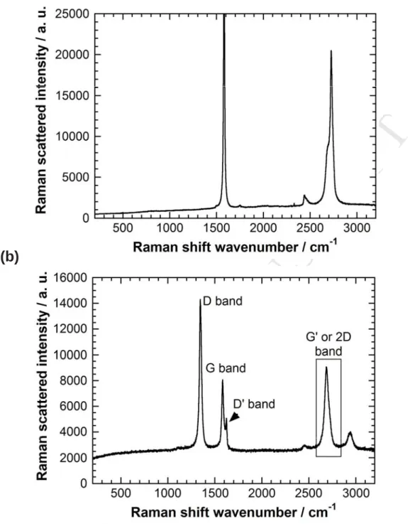
Our study draws on both the orders of Raman spectra in a multi-wavelength approach to identify the remaining carbon phases present on the gold electrode after the exfoliation processes. Raman spectra of the samples were recorded as a function of laser wavelength using different excitations, with a micro-confocal device. The Raman spectrum of the pristine natural graphite corresponds to the regular Raman signature of a perfect crystal without any measurable D and D’ bands (Fig. 4). The first Raman observations of the exfoliated gold-graphene sample demonstrated a spatial heterogeneity in the carbon film deposited on the gold electrode. With the aim of performing statistical sampling of the electrode surface area, we recorded Raman spectra mapping on a spatial area around 10 by 10 μm, with a laser spot size of 0.5 μm2 and a step of 0.2 μm. A green excitation energy of 2.41 eV was used. This choice was determined by the abundant literature obtained at this wavelength on several graphene samples [28-30]. Additionally, the second order Raman spectra exclude the possibility of turbostratic graphite phases in the sample [31]. Figure 4b displays one typical spectrum from the ~10,000 spectra taken. The second order signals dominate the spectrum. A narrow (FWHH of 25 cm-1) D band is now intense, while it was absent in the pristine graphite. The combination D’ band is also clearly visible. The width of the G band (first order at 1582 cm-1) is around 18 cm-1 against 12 for the G band of the graphite crystal. This G peak corresponds to the E2g phonon at the Brillouin zone center. The D peak due to the modes of six-atom rings (requiring defects for its Raman activation [30] comes from transverse optical (TO) phonons around the K or K’ points in the first Brillouin zone. The Raman process of this peak involves an intervalley double resonance (DR) process.
M
ANUS
C
R
IP
T
ACCEP
TED
Figure 4. a) Raman spectrum of the pristine natural graphite correspond to the regular
Raman signature of a perfect crystal without any measurable bands D and D’. b) Typical spectrum obtained after electrochemical exfoliation (2.41 eV excitation). The second order signals are labelled as D, D’ and G’ bands. The rectangle indicates the spectral range used to build the Raman map in Fig. 5. The G’ band is clearly different from the Raman profile of a G’ band characteristic of the graphite phase.
Consequently, the D band is strongly dispersive with the excitation wavelength. The D’ band (here at 1622 cm-1) also comes from a DR process but involving an intravalley process,
(a)
M
ANUS
C
R
IP
T
ACCEP
TED
al. [30], the weak value of the FWHH of G and D peaks, and the relative intensity of the D band allows us to estimate that the ratio ID/IG at around 2.1 corresponds to a distance between “defects” of around 6 nm. The profile of the second order G’ or 2D band appears in this example (Fig. 4b) as weakly asymmetric with a width of around 45 cm-1, but this profile is not representative of all the spectra. This point will be discussed on the basis of the statistics of all the spectra recorded during the Raman mappings.
Figure 5. a) Grayscale SEM picture (background) combined with the corresponding optical
image obtained by the microconfocal Raman device (foreground) showing the gold working electrode surface after electrochemical exfoliation. In red, a representative region selected for Raman mapping. b) Corresponding optical image (left), integrated Raman map obtained by selecting the spectral range between 2600 and 2800 cm-1 (right), and the two images overlaid, (centre).
Figure 5 shows an example Raman map obtained on a small and representative spatial area by selecting in the hyperspectral image the spectral range characteristic of graphene (rectangle in Fig. 4b). More precisely, the spectral range 2600-2800 cm-1 was used to integrate the signal to the baseline in order to show the spatial repartition of this integrated G’ band intensity. SEM imaging of the region used for Raman spectroscopy mapping is also shown but at low magnification (overlaid image, Fig. 5a) in order to give a clearer picture of the sample region chosen. The Raman spectra related to the blue surface area of the mapping (Fig. 5b) correspond only to the graphene phases and never to the G’ profile, which is characteristic of a graphitic phase. The area to the right of the blue domain corresponds to bare gold substrate. In the top left corner, residual deposits of carbon are found, concomitantly with Raman signals of disordered carbon or graphite phases. Note that the ratio ID/IG is obtained with a good repetition in the blue area shown in Fig 5 (ratio of 2.1 ± 0.1, giving a Ld value of 6 ±
M
ANUS
C
R
IP
T
ACCEP
TED
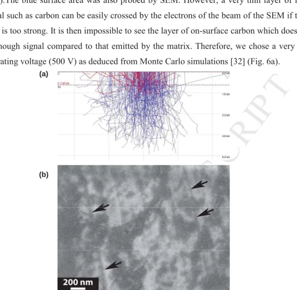
0.5 nm).The blue surface area was also probed by SEM. However, a very thin layer of light material such as carbon can be easily crossed by the electrons of the beam of the SEM if their energy is too strong. It is then impossible to see the layer of on-surface carbon which does not emit enough signal compared to that emitted by the matrix. Therefore, we chose a very low accelerating voltage (500 V) as deduced from Monte Carlo simulations [32] (Fig. 6a).
Figure 6. a) Monte Carlo simulation of electron-beam penetration assuming an accelerating
voltage of 500 V and a substrate made of pure gold covered by a thin layer of carbon (1 nm ≈ the thickness of 3 layers of graphene). b) SEM observation at low voltage (500 V) and high magnification of the gold surface after electrochemical exfoliation of the carbon coating (within the same selected region as shown in Fig. 5). The darker zones can be ascribed to the graphene deposit whereas arrows point out the scratches of the pristine gold surface.
In these conditions, already near the limits of a SEM, we have still reduced the signal received by the detector of secondary electrons by activating the build-in filter allowing selection of only secondary electrons with weak energy. There is no doubt that these adjustments allow the highlighting of regions covered with carbon but the resultant image is noisy because of the weakness of the signal finally received by the secondary electron detector. It should be noted that the strong difference in atomic number between gold and carbon makes image interpretation easier by ensuring a strong contrast between both materials even with this kind
(a)
M
ANUS
C
R
IP
T
ACCEP
TED
of detector. While the resolution of the corresponding picture is low due to this voltage, it shows a clear deposit spread onto the metallic substrate.
Faced with the quantity of Raman spectral data, we used two approaches, firstly decomposing the G’ band of the most often found signal, and secondly applying a curve separation method applied to the whole spectra of the maps (BPSS approach [21-23]). These two approaches led qualitatively to the same results. The BPSS approach shows that as well as the noisy background, only two spectra are found. Equally, decompositions on randomly selected experimental spectra can always be solved with only two kinds of source spectra. The two types of spectra, over the G’ range, are displayed in Fig. 7. They consist of either a single Lorentzian profile centered at 2685 cm-1 with a FWHH of 42 cm-1 or a more complicate profile constituted by at least four components. On the basis of the literature [24,25], we can conclude that we have a mixture at the micron scale of these two profiles. The first is assigned to the spectrum of single layer graphene (denoted 1LG), while the second is assigned to three layer graphene (denoted 3LG). The 1LG spectrum is centered at 2685 cm-1; this wavenumber is incompatible with an assignment to turbostratic graphite that displays a band at around 2710 cm-1 with a green excitation. The 3LG profile is in agreement with the profiles previously published in the literature [33].
Figure 7. The only two profiles of the G’ band of the deposited graphene sample found in the
maps of the Fig. 5. The lower red spectrum is assigned to single layer graphene 1LG excited at 514.53 nm, the upper black one is assigned to 3LG.
M
ANUS
C
R
IP
T
ACCEP
TED
Lastly, our graphene-modified gold electrode was assessed as a trap to fix organic groups either through in situ generation of free radicals or by using the charge of the graphene layer as a polynucleophilic substance essentially towards alkyl iodides. The first selected example
corresponds to the generation of 2-methylanthraquinone, via electrochemical reduction of 2-bromomethyl-anthraquinone (Br-CH2-AQ), which provokes the scission of the C-Br
bond followed by grafting onto residual graphene sheets as explained in Fig. 8a. The
corresponding CV curve of Br-CH2-AQ is shown in Fig. 8b. The first process corresponds to radical formation followed by a reversible system showing the reduction of the anthryl group. Once this electrochemical modification of the graphene interface has been performed, one obtains a reversible faradaic peak (Ep ~0.8 V, Fig. 8c,d), which can be assigned to the anthraquinone redox moiety. The large modification of the electrochemical signature of graphene (for potentials lower than < -1.7 V, Fig. 8c) would suggest the grafting of AQ• concerns not only the edges of the capping but a large part of graphene itself. A simple comparison between CV curves reported in Fig. 2a and Fig. 8c, respectively, for which similar experimental conditions were used, strongly supports this assumption.
Figure 8. a) Expected cathodic cleavage of 2-bromomethyl-anthraquinone followed by
grafting onto residual graphene sheets. b) Addition of 2-methylanthraquinone free radical via the cathodic cleavage of Br-CH2-AQ obtained in situ at a Au-graphene surface between 0 and -1.2 V (the first main faradaic peak corresponds to the scission of the C-Br bond). Electrolyte: 0.1 M TEABF4 in DMF; v = 50 mV s-1. c) CV curves of the resulting modified electrode after careful rinsing in water, and acetone. The electrochemical response of the surface is dramatically changed: first, a reversible faradaic peak is noted at ≈-0.8 V assigned to the reversible two-electron reduction of anthraquinone (AQ). Second, the specific response of the graphene deposit is strongly modified as compared to Fig. 2a beyond -1.7 V. This is assigned to a partial modification of the graphene network after a dispersed addition of
AQ-M
ANUS
C
R
IP
T
ACCEP
TED
CH2 radicals. The surface concentration of AQ is estimated to 9.2 × 10 mol cm (first scan). d) Voltammetric response of the grafted AQ moiety measured at 100 mV s-1.
The second example relies on the grafting of a marked alkyl iodide by ferrocene as illustrated in Fig. 9. Two modes of catalysis are possible. The first, centred at about -1 V, corresponds to catalysis by gold that permits the scission of the C-I bond (by a specific adsorption). The second involves a nucleophilic process (charge of graphene at about -2 V). These two successive processes are easily visible in Fig. 9b. Note that for comparison, the plot also includes the response of the electrode without modification by graphene coverage. The response of the electrode after alteration is shown in Fig. 9b (oxidation of the grafted ferrocene moiety). Finally, Fig. 9c shows the response of a graphene free gold electrode and the catalytic scission of the C-I bond located at about -1 V.
Figure 9. a) Expected cathodic cleavage of 2-bromomethyl-anthraquinone followed by
grafting onto residual graphene sheets. Evidence of addition of the ferrocene moiety (Fc) onto the graphene network of a graphene-modified gold electrode (electrolyte: 0.1 M TEABF4 in
M
ANUS
C
R
IP
T
ACCEP
TED
DMF; v = 50 mV s-1). a) Response of the electrode with and without Fc-C6-I (C = 8 mmol L -1). The deposit of Fc-C6 is achieved thanks to a pair of scans between 0 and -2.2 V. b) Response (oxidation of ferrocene into ferrocenium cation) of the grafted ferrocene. Two successive scans. c) For comparison, a voltammetric response in the condition of a) without graphene deposit (blank experiment). The sole visible process is the catalytic peak (around -1 V) of the alkyl iodide onto Au also visible in one scan in a).
4. Conclusions
To conclude, this work shows for the first time experimental proof that our simple and practical exfoliation process creates a gold electrode with surface adsorbed graphene consisting of either 1 or 3 layers (but not two). These graphene-modified gold electrodes were then used as a trap to fix organic groups either through in situ generation of free radicals, or by using the charge of the graphene layer as a polynucleophilic substance essentially towards alkyl iodides. The simplicity, scalability and chemical tuneability of this approach gives it many advantages over current conventional carbonaceous electrodes. Simple electrochemical exfoliation of any kind of graphite, achieved by its reduction at about -2.0 V, certainly represents a fascinating method for in situ generating thin graphene layers at electrified solid substrates. Moreover, it could be extendable to other solid conductors (silver, rhodium, copper, platinum and palladium) [34]. Based on this series of data, it can be underlined that the formation of either mono- or tri-layer graphene on Au, but no bi-layer, is most surprising. The behaviour is reminiscent of a Stage-2 graphite intercalation compound, however solution-based ion intercalation of TAA+ in graphite results in Stage-1 compounds (i.e. ion intercalation between every graphene layer) [15]. It is possible the “Stage-2”-like behaviour we observe comes from the asymmetry induced by the electrode, and consequent alternate polarization of the graphene layers. This would give a positively charged outer layer for bilayer graphene, energetically unfavourable for TAA+ interaction. Such capacitive polarisation has been documented previously in the literature, for example in the capacitive response of bilayer graphene in the presence of a top-gate [35]. The presence of the gold is critical, since TAA+ electrochemistry of graphite electrodes results in thicker (~2 nm) flakes [16]. However further studies on well orientated crystallized gold substrates will be needed to fully understand this effect.
M
ANUS
C
R
IP
T
ACCEP
TED
References[1] McCreery R L. Advanced carbon electrode materials for molecular electrochemistry. Chem Rev 2008;108(7):2646-2687.
[2] Simonet J, Lund H. Electrochemical behavior of graphite in the presence of tetraalkylammonium cations. J Electroanal Chem Interfacial Electrochem 1977;75(2):719-730.
[3] Dano C, Simonet J. Cathodic reactivity of graphite with carbon dioxide: an efficient formation of carboxylated carbon materials. J Electroanal Chem 2004;564(15):115−21.
[4] Jenkins G M, Kawamura K. Structure of glassy carbon. Nature 1971;231:175-176.
[5] Harris P J F. Fullerene-related structure of commercial glassy carbons. Philos Mag 2004;84(29):3159-3167.
[6] Jouikov V, Simonet J. Novel method for grafting alkyl chains onto glassy carbon. Application to the easy immobilization of ferrocene used as redox probe. Langmuir 2012;28(1):931-938.
[7] Jouikov V, Simonet J. Electrochemical conversion of glassy carbon into a poly-nucleophilic reactive material. Applications for carbon chemical functionalization. a mini-review. Electrochem Commun 2014;45:32-36.
[8] Novoselov K S, Geim A K, Morozov S V, Jiang D, Zhang Y, Dubonos, S. V. et al. Electric field effect in atomically thin carbon films. Science 2004;306(5696):666-669.
[9] Geim A K, Novoselov K S. The rise of graphene. Nat Mater 2007;6:183-191.
[10] Geim A K. Graphene: status and prospects. Science 2009;324(5934):1530-1534.
[11] Yang X Y, Dou X, Rouhanipour A, Zhi L J, Rader H J, Mullen K. Two-dimensional graphene nanoribbons. J Am Chem Soc 2008;130(13):4216-4217.
[12] Ambrosi A, Chua C C, Bonanini A, Pumera M. Electrochemistry of graphene and related materials. Chem Rev 2014;114(14):7150-7188, and references cited.
M
ANUS
C
R
IP
T
ACCEP
TED
[13] Sirisaksoontorn W, Adenuga A A, Remcho V T, Lerner M M. Preparation and characterization of a tetrabutylammonium graphite intercalation compound. J Am Chem Soc 2011;133(32):12438-12438.
[14] Zhong Y L, Swager T M. Enhanced electrochemical expansion of graphite for in situ electrochemical functionalization. J Am Chem Soc 2012;134(43):17896-17899.
[15] Sirisaksoontorn W, Lerner M M. Preparation of a homologous series of tetraalkylammonium graphite intercalation compounds. Inorg Chem 2013;52(12):7139-7144.
[16] Cooper A J, Wilson N R, Kinloch I A, Dryfe R A W. Single stage electrochemical exfoliation method for the production of few-layer graphene via intercalation of tetraalkylammonium cations. Carbon 2014;66:340-350.
[17] Yang Y, Lu F, Zhou Z, Song, W, Chen Q, Ji X. Electrochemically cathodic exfoliation of graphene sheets in room temperature ionic liquids n-butyl, methylpyrrolidinium bis(trifluoromethylsulfonyl)imide and their electrochemical properties. Electrochim Acta 2013;113: 9-16.
[18] Low C T J, Walsh F C, Chakrabarti M H, Hashim M A, Hussain M A. Electrochemical approaches to the production of graphene flakes and their potential applications. Carbon 2013;54:1-21.
[19] Simonet J. Composite materials {glassy carbon/graphene/zero-valent metal (Pd0)} for building three-dimensional redox electrodes. Electrochem Commun 2014;42: 34-37.
[20] Jouikov V, Simonet J. Efficient cathodic carboxylation of graphene: building a new versatile material. Electrochem Commun 2014;43:67-70.
[21] Moussaoui S, Brie D, Carteret C, Mohammad-Djafari A. Application of Bayesian non-negative source separation to mixture analysis in spectroscopy. In: Fischer R, Preuss R, von Toussaint U, editors, International Workshop on Bayesian Inference and Maximum Entropy Methods in Science and Engineering (MaxEnt’2004), vol 735, Institute of Physics; p. 237-244.
M
ANUS
C
R
IP
T
ACCEP
TED
[22] Quilès F, Nguyeng-Trung C, Carteret C, Humbert B. Hydrolysis of uranyl(vi) in acidic and basic aqueous solutions using a noncomplexing organic base: A multivariate spectroscopic and statistical study. Inorg Chem 2011;50(7):2811-2823.
[23] Carteret C, Dandeu A, Moussaoui S, Muhr H, Humbert B, Plasari E. Polymorphism studied by lattice phonon Raman spectroscopy and statistical mixture analysis method. application to calcium carbonate polymorphs during batch crystallization. Cryst Growth Des 2009;9(2):807-812.
[24] Ferrari A C, Meyer J C, Scardaci V, Casiraghi C, Lazzeri M, Mauri F et al. Raman spectrum of graphene and graphene layers. Phys Rev Lett 2006;97(18):187401.
[25] Ferrari A, Basko D. Raman spectroscopy as a versatile tool for studying the properties of graphene. Nat Nanotechnol 2013;8:235-246.
[26] Baranov A V, Bekhterev A N, Bobovich Y S, Petrov V I. Interpretation of certain characteristics in Raman spectra of graphite and glassy carbon. Opt Spectrosk 1987;62(5):1036-1042.
[27] Thomsen C, Reich S. Double resonant Raman scattering in graphite. Phys Rev Lett 2000;85(24):5214-5217.
[28] Park J S, Reina A, Saito R, Kong J, Dresselhaus G, Dresselhaus M S. G’ band Raman spectra of single, double and triple layer graphene. Carbon 2009;47:1303-1310.
[29] Lucchese M M, Stavale F, Martins Ferreira E H, Vilani C, Moutinho M V O, Capaz R B et al. Quantifying ion-induced defects and Raman relaxation length in graphene. Carbon 2010;48:1592-1597.
[30] Cançado L G, Jorio A, Martins Ferreira E H, Stavale F, Achete C A, Capaz R B et al. Quantifying defects in graphene via Raman spectroscopy at different excitation energies. Nano Lett 2011;11(8):3190-3196.
[31] Wilhelm H, Lelaurain M, McRae E, Humbert B. Raman spectroscopic studies on well-defined carbonaceous materials of strong two-dimensional character. J Appl Phys 1998;84(12):6552-6558.
M
ANUS
C
R
IP
T
ACCEP
TED
[32] The ‘Casino’ program for "monte CArlo SImulation of electroN trajectory in sOlids", see http://www.gel.usherbrooke.ca/casino/What.html (accessed December 2015).
[33] Malard L M, Pimenta M A, Dresselhaus G, Dresselhaus M S, Raman spectroscopy in graphene, Phys Rep 2009;473:51-87.
[34] Jouikov V, Stéphant N, Poizot P, Simonet J. The silver–graphene electrode. building, stability, and catalytic efficiency. Electrochem Commun 2015;51:125-128.
[35] Young A F, Levitov L S. Capacitance of graphene bilayer as a probe of layer-specific properties. Phys Rev B 84, 085441 (2011))