HAL Id: hal-00513756
https://hal.archives-ouvertes.fr/hal-00513756
Submitted on 1 Sep 2010
HAL is a multi-disciplinary open access archive for the deposit and dissemination of sci-entific research documents, whether they are pub-lished or not. The documents may come from
L’archive ouverte pluridisciplinaire HAL, est destinée au dépôt et à la diffusion de documents scientifiques de niveau recherche, publiés ou non, émanant des établissements d’enseignement et de
Didier Kempf, Vincent Vignal, Georges Cailletaud, Roland Oltra, J.C.
Weeber, Eric Finot
To cite this version:
Didier Kempf, Vincent Vignal, Georges Cailletaud, Roland Oltra, J.C. Weeber, et al.. High spatial resolution strain measurements at the surface of duplex stainless steels. Philosophical Magazine, Taylor & Francis, 2007, 87, pp.1379-1399. �10.1080/14786430600928527�. �hal-00513756�
For Peer Review Only
High spatial resolution strain measurements at the surface of duplex stainless steels
Journal: Philosophical Magazine & Philosophical Magazine Letters Manuscript ID: TPHM-06-Jan-0023.R1
Journal Selection: Philosophical Magazine Date Submitted by the
Author: 09-Jun-2006
Complete List of Authors: Kempf, Didier; LRRS, Chemistry Vignal, Vincent; LRRS, chemistry
Cailletaud, Georges; Centre des Matériaux, ENSMP Oltra, Roland; LRRS, Chemistry
Weeber, Jean Claude; LPUB, Physics finot, eric; LPUB, Physics
Keywords: alloys, deformation, dislocations, free surface, mechanical behaviour, micromechanics, nanomechanics, plasticity of metals Keywords (user supplied):
For Peer Review Only
High spatial resolution strain measurements
at the surface of duplex stainless steels
D. Kempf1, V. Vignal1,*, G. Cailletaud2, R. Oltra1, J.C. Weeber3, and E. Finot3
1 LRRS, UMR 5613 CNRS – Université de Bourgogne, BP 47870, 21078 Dijon, France
2 Centre des Matériaux, UMR 7633 CNRS – Ecole des Mines de Paris, BP 87, 91003 Evry, France
3 LPUB, UMR 5027 CNRS – Université de Bourgogne, BP 47870, 21078 Dijon, France
Abstract
The determination of local strain fields at the surface of materials is of major importance for understanding their reactivity. In the present paper, lithography is used to fabricate grid points at the microscale and to map strain gradients within grains and between grains. This method was applied to duplex stainless steels which exhibit heterogeneous strain distributions under straining conditions. The influence of various parameters (the specimen microstructure, the density of slip bands, the number of systems activated and the grid geometry) on the strain value was discussed.
Keywords : local extensometry, strain, duplex stainless steel, microstructure 3 4 5 6 7 8 9 10 11 12 13 14 15 16 17 18 19 20 21 22 23 24 25 26 27 28 29 30 31 32 33 34 35 36 37 38 39 40 41 42 43 44 45 46 47 48 49 50 51 52 53 54 55 56 57 58 59
For Peer Review Only
1. Introduction
Duplex stainless steels are highly important engineering materials, due to their generally high corrosion resistance and their high strength and toughness. They have a complex microstructure with comparable volume of austenite and ferrite. Due to differences in mechanical properties, a heterogeneous strain distribution is generated in both phases under straining conditions and the presence of these surface strain gradients may affect the physico-chemical properties of the material. Therefore, it is of major importance to quantify surface strains at the microstructure scale.
Atomic force microscopy (AFM) offers the possibility to examine the 3D surface morphology in order to evaluate in-plane changes (up to 150 × 150 µm2) and to measure out-of-plane differences (up to 6 µm) at the microscale. AFM has been used to study the surface topography of fatigued stainless steels, especially in kinetic study of growth where the shape of extrusions and intrusions has been followed as a function of the number of loading cycles [1-2]. Description of plastic deformation processes and strain gradients around grain boundaries has also been proposed after uniaxial tensile loading [3-4]. These studies remain qualitative and only a few parameters, such as the surface roughness and the steps height, have been determined as a function of applied strain. However, combining AFM with the electron back-scatter diffraction (EBSD) has permitted to show that the surface roughness and the misorientation of grains increase linearly with increasing applied strain [5-8].
Regarding quantitative approaches, a stereoimaging technique (including a Cognex 2000 image processing system, cameras to obtain digital images from analog photographs, a graphics display terminal, a track ball for operator interaction with the system and a video display monitor for display of the measured displacements) has been developed to perform 3 4 5 6 7 8 9 10 11 12 13 14 15 16 17 18 19 20 21 22 23 24 25 26 27 28 29 30 31 32 33 34 35 36 37 38 39 40 41 42 43 44 45 46 47 48 49 50 51 52 53 54 55 56 57 58 59 60
For Peer Review Only
measurements of microdisplacements under high resolution conditions [9]. Microscopic strain mapping using SEM topography image correlation at large strain was also performed on aluminum alloys and relationships between slip lines, dynamic strain aging, shear localization, diffuse and localized necking were obtained [10-11]. In addition, object grating methods have been proposed for evaluating local strains in multiphase or composite materials in which the microstructural scale is in the order of tens micrometers and at microstructural inhomogeneities such as grain boundaries and crack tips. However, all the authors have claimed that the complexity of the experimental strain distribution is better explained by the complementary use of a finite element model. The effect of grain boundary deformation on the creep micro-deformation of pure copper [12], the influence of the presence of A1203 particles in aluminium alloys [13] and the behaviour of iron/silver and iron/copper blends [14] have been studied under uniaxial tensile stress. On the other hand, composite Ag-Ni materials have been tested under uniaxial compression [15].
A similar technique has been applied to duplex stainless steels at the mesoscale with a gauge length of about 50 µm [16]. The strain in the loading direction was found to vary significantly from one grain to another, and inside grains, from 2.2 % to 6.2 % for an applied strain of 4.5 %. By contrast, the strain in the direction perpendicular to loading was smaller and remained more-or-less constant over a large number of grains (compression of about -1.3 %). This was attributed to the fact that swelling of grains in this direction was restricted by the constraints imposed by neighbouring grains. It has also been shown that the surface roughness increases linearly with the out-of-plane strain component. In the present paper, surface strains were mapped at the microscale on duplex stainless steels and the role of the microstructure on the existence of microstrain gradients was discussed. This implied the development of grids 3 4 5 6 7 8 9 10 11 12 13 14 15 16 17 18 19 20 21 22 23 24 25 26 27 28 29 30 31 32 33 34 35 36 37 38 39 40 41 42 43 44 45 46 47 48 49 50 51 52 53 54 55 56 57 58 59
For Peer Review Only
pads, distance between two successive pads, gauge length, etc.), on the strain value was also discussed. In addition, the proposed method has revealed the strain heterogeneities induced by the emergence of slip bands and has allowed an experimental quantification of the activity of these systems in both metallic phases.
2. Experimental
2.1. Tensile specimens and surface preparation
Experiments were performed on a duplex stainless steel (UNS S31803, chemical composition : C : 0.02wt.%; Mn : 1.62%; Ni : 5.45%; Cr : 22.44%; Mo : 2.92%; N : 0.17% and Si : 0.39%). It was hot rolled to obtain 20 mm thick sheets, solution annealed at 1050°C for 15 min and water quenched. Specimens showed a lamellar microstructure with a grain size of about 5 µm in the lamellar direction, as shown in Fig. 1(a). In order to increase the grain size, a second heat treatment was carried out consisting of a homogenization treatment at 1300°C for 1 hour, followed by a slow cooling down to 1080°C (formation of the austenite) and a water quenching. The volume fraction of austenite and ferrite was evaluated to 50/50 and the grain size was about 75 µm, as shown in Fig. 1(b). The 0.2% yield strength (Rp0.2) and the ultimate strength (Rm) of this material were 560 and 760 MPa at 25°C, respectively.
Tensile specimens were machined in order to have a cross-section of 2 × 6 mm2 and a gauge length of 25 mm, as shown in Fig. 2(a). They were mechanically ground using emery papers and polished using diamond pastes (down to 1 µm). The average surface roughness was then evaluated to about 5 nm (calculated on 50 × 50 µm2 areas).
2.2. Elaboration of the grid points
3 4 5 6 7 8 9 10 11 12 13 14 15 16 17 18 19 20 21 22 23 24 25 26 27 28 29 30 31 32 33 34 35 36 37 38 39 40 41 42 43 44 45 46 47 48 49 50 51 52 53 54 55 56 57 58 59 60
For Peer Review Only
A conventional process of electron beam lithography was used as described in Ref [16]. A 300 nm depth resin film (PMMA) was spin coated on the gauge surface of tensile specimens before being baked for 3 hours at 175 °C in order to become stiff. An electron beam microscope was used to mark the surface by local chemical damages in the resin layer. The electron beam microscope was a Jeol 6500F and was coupled with a beam position controller software (Raith Elphy Quantum). Chemically modified zones of the layer were attacked preferentially in a first solvent solution for a few seconds with ultrasonic waves. Then, this development stage was stopped in second solvent bath with ultrasonic waves and the tensile specimens were then blown dry with pure nitrogen. A first layer of about 50 nm nickel was then deposited in an electron gun evaporator and recovered in a thermal evaporator by a second layer of 10 nm gold. Nickel was chosen because of its good adherence on metallic substrates and the thin layer of gold was deposited in order to locate easily the 20 arrays of pads on the gauge surface from optical observations, as schemed in Fig. 2(b). The last stage consists of a lift-off : the remaining resin was removed and the metallic (Ni and Au) pads became apparent. Finally, the sample was blown dry with pure nitrogen.
2.3. Mechanical tests and surface observations at the microscale
Tensile specimens were then subjected to uniaxial tensile loading in air at 4.6% plastic strain applied along the X1-axis using a home-made tensile microstage. Surface observations were performed after unloading using a field-emission type scanning electron microscope (FE-SEM, JEOL 6400F).
3. Results and discussion
The in-plane strain components were evaluated from the average distance between 3 4 5 6 7 8 9 10 11 12 13 14 15 16 17 18 19 20 21 22 23 24 25 26 27 28 29 30 31 32 33 34 35 36 37 38 39 40 41 42 43 44 45 46 47 48 49 50 51 52 53 54 55 56 57 58 59
For Peer Review Only
L L L 0 , 1 0 , 1 1 11 −−−− ==== ε , L L L 0 , 2 0 , 2 2 22 −−−− ==== ε (1)where L1 and L2 are the average distances between centroids of pads along the X1- and X2 -axis, respectively, after deformation and L1,0 and L2,0 are the average distances before deformation. The distance between centroids of pads was measured from section profiles (obtained from FE-SEM images) which were smoothed using a lowpass frequency filter (f > 1 Hz). When a pad was located straight above a slip band, peeling may occur and therefore no strain measurement was carried out.
3.1. Characteristics of the grid points and high spatial resolution strain measurements
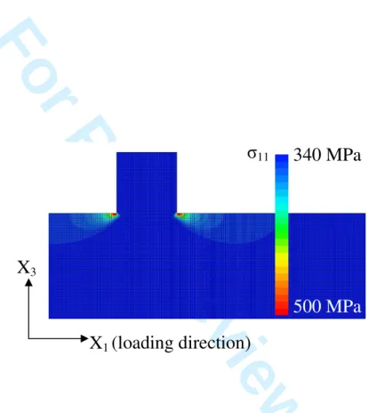
Mapping microstress gradients within grains and across the austenite/ferrite interface on the globular microstructure shown in Fig. 1(b) requires the use of specific grids. In this case, the gauge length must be smaller than 10 µm (to have several values within a grain) and the distance between two points of measurement must be smaller than 1 µm (to have a good spatial period for computation). In order to optimize these parameters, the influence of pads on the surface stress field was investigated under straining conditions by means of numerical simulation. The substrate was assumed to be pure austenite having an isotropic elastic-plastic behaviour (the elastic-plastic material model used was determined by fitting experimental stress-strain curves obtained until the ultimate stress with the finite element method model). On the other hand, pads were assumed to be pure nickel having an elastic behaviour (the surface stress around pads is then slightly overestimated). QUAD4 elements composed of four nodes located at the four geometric corners of quadrangles were used in the meshing and the density of elements was chosen such that each pad was composed of 35×35 elements. To prevent undesirable edge effects, the substrate thickness was ten times larger than the diameter of pads. Regarding the boundary conditions, the vertical and horizontal 3 4 5 6 7 8 9 10 11 12 13 14 15 16 17 18 19 20 21 22 23 24 25 26 27 28 29 30 31 32 33 34 35 36 37 38 39 40 41 42 43 44 45 46 47 48 49 50 51 52 53 54 55 56 57 58 59 60
For Peer Review Only
The loading (360 MPa, corresponding roughly to 4.6 % plastic strain) was applied to the left edge of the region analysed. Significant stress concentrations were observed around pads and these gradients extend over a distance of about twice the diameter of pads, as shown in Fig. 3. Therefore, in order to prevent interactions between pads that would affect the results, the ratio of the distance between pads to the diameter of pads must be chosen at least equal to 4.
Considering these limitations (gauge length smaller than 10 µm and ratio of the distance between pads to the diameter of pads greater than 4), the diameter and the height of pads were fixed to 70 nm and the distance between pads was set at 730 nm in the two directions. Numerous surface observations on the unstrained specimens showed that the fabrication process induced a dispersion of ± 4.5 nm on the distance between pads. As the size of these pads was of the same order of magnitude as the radius of curvature at the tip apex, AFM images revealed distorted pads from which no accurate measurements could be performed. The mechanical analysis was then carried out from FE-SEM images recorded at a magnification of 14,000 (8.59×6.87 µm2), as shown in Fig. 2(c). At this resolution, the pixel size was 6.7 nm for an image size of 1280×1024 pixels.
It has to be pointed out that the error made on the determination of the pad position was estimated to ±1 pixel. The relative errors in percentage of the exact value of strain were estimated from Equation (2) to about ±1.84 % and ±0.26 % for a gauge length of 0.73 µm and 5.11 µm, respectively. 100 ) ( _ ) ( _ ) ( _ 2 (%) = ± × × µm length gauge µm size image px resolution image error (2)
The resolution in strain can be significantly improved by measuring the average distance 3 4 5 6 7 8 9 10 11 12 13 14 15 16 17 18 19 20 21 22 23 24 25 26 27 28 29 30 31 32 33 34 35 36 37 38 39 40 41 42 43 44 45 46 47 48 49 50 51 52 53 54 55 56 57 58 59
For Peer Review Only
value of strain was decreased down to about ±4.5/(8×730) = 0.08 %. Therefore, the method proposed is suitable for mapping plastic strains at the microscale (above 15 % plastic strain, the surface roughness becomes too high and cannot be neglected in the strain calculation [14]) and for quantifying elastic strains at the mesoscale.
3.2. Strain field around a slip band and effects of the gauge length on the strain value
In order to map the strain field around slip bands in the loading direction, several values of ε11 were measured along straight lines, from the point A to the point B in Fig. 4, using a gauge length of 0.73 µm (the strain was measured between two successive pads). In the absence of any visible slip bands crossing the line A-B, ε11 was found to be constant. In the case of Fig. 4(a), a value of about 3 % was derived from the calculation, as shown in Fig. 5(a). By contrast, a sharp increase of ε11 was observed straight above slip bands, as shown in Figs. 4(b)-(c) and 5(b)-(c), indicating that the strain concentration induced by these line defects extends over a very short distance. Therefore, quantifying the strain field around surface defects (such as slip bands, grain boundaries and interfaces between metallic phases) requires the use of high spatial resolution methods. It can also be noticed that the larger the slip band, the higher the maximum strain value reached (of about 8.9 % in Fig. 5(b) for the small slip band visible in Fig. 4(b) and 15.2 % in Fig. 5(c) for the large slip band visible in Fig. 4(c)) and that the highest strain value obtained was about three times greater than the applied strain (of about 4.6 %).
It is also interesting to note that ε11 may not be constant along a slip band. The value of ε11 was found to vary along the slip band SB1 reported in Fig. 4(b) from 8 % plastic strain at the point C up to about 13 % at the point D whereas the distance between the two points 3 4 5 6 7 8 9 10 11 12 13 14 15 16 17 18 19 20 21 22 23 24 25 26 27 28 29 30 31 32 33 34 35 36 37 38 39 40 41 42 43 44 45 46 47 48 49 50 51 52 53 54 55 56 57 58 59 60
For Peer Review Only
was around 8 µm as shown in Fig. 5(d). This indicates that high strain gradients may exist along such line defects (of about 0.6 %/µm in average for the slip band SB1).
The influence of the gauge length on the strain value was then studied within the three same sites in order to determine the pertinent scale of analysis and to correlate the results to physically meaningful quantities. The gauge length varied from 5.11 µm (distance between the points A and B in Fig. 4 including seven intervals between pads) down to 0.73 µm (distance between the points A’ and B’ in Fig. 4 including one interval between pads) while the position of measurement was maintained unchanged (corresponding to the cross in Fig. 4). The strain measured over a distance including several intervals between pads, ( )(%)
11
N
ε , was equal to the average of the strains determined on each interval (with a gauge length of 0.73 µm) :
(
)
+ + = =∑
+ = = = = = 2 / ) 1 ( 2 ) 1 ( , 11 ) 1 ( , 11 ) 1 ( 1 , 11 ) ( 11 ) 1 ( 1 , 11 ) 1 ( 11 * 1 (%) (%) N i N i N i N N N N ε ε ε ε ε ε (3)where N (= 3, 5 or 7) is the number of intervals between pads considered (the gauge length is then given by N×0.73 (µm)), ( 1)(%) , 11 = N i ε and *( 1)(%) , 11 = N i
ε are the strains measured on both sides
of the slip band with a gauge length of 0.73 µm (see the scheme insert in Fig. 4). Fig. 5 (e)-(j) shows that the strains measured for different gauge lengths are in an excellent agreement with the strains calculated using Equation (3), indicating that the method proposed gives accurate results for a wide range of gauge lengths. Furthermore, this indicates that the error made using a 0.73 µm gauge length was significantly lower than the value determined from Equation (2). This error was at least as small as the error calculated for a gauge length of 5.1 µm (of about 0.26%). For gauge lengths above 3.65 µm, the strain was constant, as shown in Fig. 5 (e)-(j), 3 4 5 6 7 8 9 10 11 12 13 14 15 16 17 18 19 20 21 22 23 24 25 26 27 28 29 30 31 32 33 34 35 36 37 38 39 40 41 42 43 44 45 46 47 48 49 50 51 52 53 54 55 56 57 58 59
For Peer Review Only
of grains. On the other hand, strain values obtained for small gauge lengths (generally 0.73 µm) could be used to describe the local strain state generated by single slip bands (Figs. 5 (f) and (g)).
3.3. Mapping the surface strain field within grains after unloading
The influence of high microstrain concentrations induced by single slip bands was neglected by setting the gauge length at 5.11 µm (see Fig. 5 (e)-(j)). Fig. 6 shows the dispersion of ε11 and ε22 obtained within 18 grains of the duplex stainless steel. It can be noticed that several values of strains were evaluated in some grains.
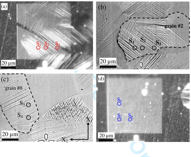
Regarding ε11, the average strain calculated considering all the investigated grains was equal to 4.8 %, as shown in Fig. 6(a), which is very close to the applied permanent plastic strain (of about 4.6 %). This result tends to validate the method proposed. Significant differences in the mechanical behaviour of the two phases were observed. Austenite was found to undergo more tension (6 % plastic strain in average in this phase) than the ferrite (3.7 % plastic strain in average). These results were confirmed by means of FE-SEM observations which revealed that slip bands were preferentially located in austenite. In addition, the strain field developed under straining conditions at the surface of the austenitic grains was highly heterogeneous and values between 3.6 % and 9.7 % were found, as shown in Fig. 6(a). These large variations in strain were detected between grains and within grains. For example, ε11 varied from 6.2 % up to 9.7 % within the grain #10 and from 4.5% up to 7.9 % within the grain #2. In the former case, the largest strain value was obtained within the site S1 where numerous slip bands emerged, as shown in Fig. 7(a), whereas the lowest strain values were systematically measured on sites with a low density of slip bands (such as the sites S2 and S3 reported in Fig. 7(a)). As the distance between these two kinds of sites is small (of about 3 4 5 6 7 8 9 10 11 12 13 14 15 16 17 18 19 20 21 22 23 24 25 26 27 28 29 30 31 32 33 34 35 36 37 38 39 40 41 42 43 44 45 46 47 48 49 50 51 52 53 54 55 56 57 58 59 60
For Peer Review Only
10 µm between S1 and S2), large strain gradients are expected in the austenite and these gradients may affect the physico-chemical properties and the pitting resistance of duplex stainless steels.
Some austenite grains were under compression along the X2-axis (due to Poisson’s effects) and it appears that the more positive the value of ε11, the more negative the value of ε22 (see the sites S1, S2 and S3 within the grain #2 in Figs. 6 and 7). It can be mentionned that such grains are generally oriented perpendicularly to the loading direction (X1-axis), as shown in Fig. 7(b). By contrast, most of the grains elongated along the X1-axis (such as the grain #8 visible in Fig. 7(c)) were found to be slightly in tension along the X2-axis (values of ε22 between 0 and 2.8 % for the grains #8, #9, #10, #14 and #17 in Fig. 6(b)).
Ferrite was submitted to a more uniform strain field than austenite, although it was possible to observe large slip bands in some sites (attributed to the neighboring and underneath grain effects). Values of ε11 between 2.3 % and 5.9 % were derived from the calculation, as shown in Fig. 6(a). Strain values in the range of 2.3 % to 3.7 % (average strain in this phase) were mainly obtained on sites free of any visible slip bands (such as the sites S6, S7 and S8 reported in Fig. 7(d)) whereas slip bands were often observed on grains where strains greater than 3.7 % were found. In addition, it can be observed that 6 grains out of the 9 grains analysed exhibit negative values of ε22, indicating that ferrite is mainly under compression along the X2-axis.
3.4. Mapping the surface strain gradients across the austenite/ferrite interface
The results presented previously suggest that high strain gradients exist at the surface 3 4 5 6 7 8 9 10 11 12 13 14 15 16 17 18 19 20 21 22 23 24 25 26 27 28 29 30 31 32 33 34 35 36 37 38 39 40 41 42 43 44 45 46 47 48 49 50 51 52 53 54 55 56 57 58 59
For Peer Review Only
accurately these gradients. The path to be investigated was first selected according to the microstructure (across the austenite/ferrite interface) and the process of deformation (density and morphology of slip bands, number of systems activated). A set of images (8.59×6.87 µm2) was then recorded along this path using FE-SEM and it has to be mentioned that two successive images had always some columns of pads in common (imaging with FE-SEM induces a small deposition of carbon at the specimen surface which makes easier the localisation of the edge of each image). The mechanical analysis explained in the previous sections was applied along the path using different gauge lengths (5.11 µm and 0.73 µm).
3.4.1. Mapping in the absence of large slip bands
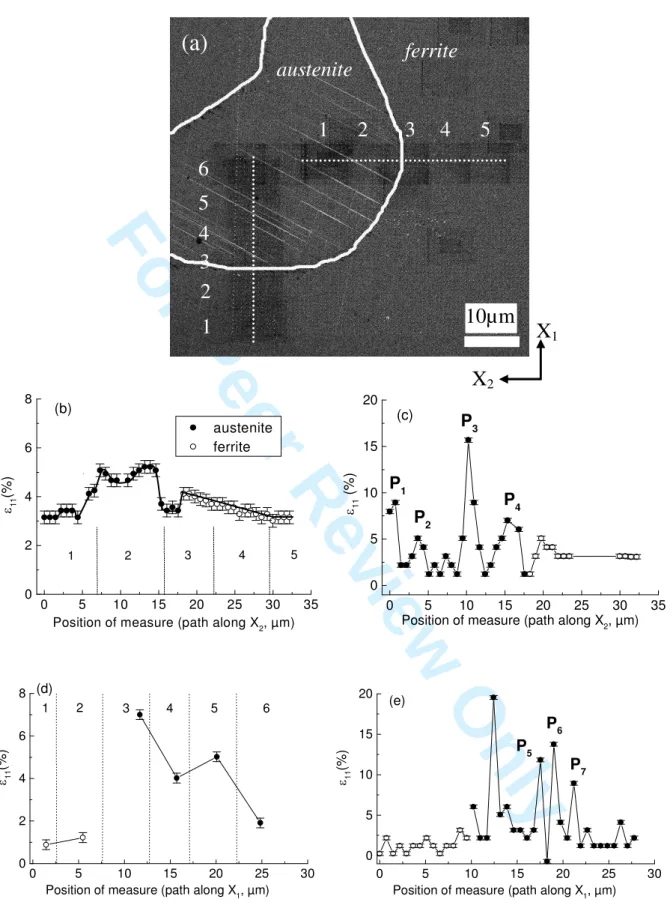
Evolution of ε11 along the X2-axis. Particular attention was first paid to the distribution of ε11 along the X2-axis. The mechanical analysis was performed on six images recorded on both sides of the interface in a region free of any large slip bands, as shown in Fig. 8(a). Only a few small slip bands were present in austenite (Figs. 9(a) and (b)) while slightly larger slip bands were found to emerge at the ferrite surface (Fig. 9(c)).
Roughly the same evolution of ε11 was obtained for the two gauge lengths, as shown in Figs. 8(b) and (c). Smooth variations of ε11 were observed in the austenite for a gauge length of 5.11 µm (Fig. 8(b)). This was certainly due to the emergence of a high density of extremely small slip bands which can not be detected by FE-SEM. The lowest strain value, of about 3.6 %, was found in a region between the images #1 and #2 in Fig. 9(a) and the highest strain value, of about 5.4 %, was obtained close to the interface (image #3 in Fig. 9(b)). The presence of numerous small peaks when decreasing the gauge length (Fig. 8(c)) was attributed to the increasing influence of the small slip bands detected by FE-SEM on the strain value (such as the peak P1 related to the slip band visible in Fig. 9(b)). By contrast, a large plateau 3 4 5 6 7 8 9 10 11 12 13 14 15 16 17 18 19 20 21 22 23 24 25 26 27 28 29 30 31 32 33 34 35 36 37 38 39 40 41 42 43 44 45 46 47 48 49 50 51 52 53 54 55 56 57 58 59 60
For Peer Review Only
corresponding to 3 % plastic strain was observed in the ferrite far from the interface (image #5 in Fig. 9(c)), confirming that the strain field in this phase was quite uniform. The strain in ferrite increases sharply when approaching the interface in order to accommodate with the austenite strain state (5.4 % plastic strain on both sides of the interface).
Evolution of ε11 along the X1-axis. The in-plane component ε11 of the strain tensor was found to be more-or-less constant along the X1-axis (between 3 % and 4 % plastic strain in Figs. 8(d) and (e)), suggesting that no significant strain gradients exist across the austenite/ferrite interfaces oriented perpendicularly to the loading direction. Therefore, the specimen microstructure (morphology of grains) plays a major role in the location of strain gradients at low plastic strain levels. However, the peaks related to the existence of small slip bands were again observed using a gauge length of 0.73 µm, as shown in Fig. 8(e).
Evolution of ε22 along the X1- and X2-axis. The values of ε22 obtained along the two paths investigated were highly negative. Since the absolute value of ε22 is larger than ε11, this cannot be related only to a normal contraction due to Poisson’s effect in the elastic law, and isochoric plastic flow : in fact, the local stress state is far from being onedimensional. There is a compressive stress σ22. In addition, only minor fluctuations of ε22 were observed in these directions (Figs. 10(b) and (d)) and individual slip bands generated very small peaks (Figs. 10(c) and (e)), confirming that the swelling of grains along the X2-axis was restricted by the constraints imposed by neighbouring grains. As a consequence, the in-plane component ε11 only would be the relevant parameter for describing the influence of mechanical strains on the reactivity of solids at low plastic strain levels.
3 4 5 6 7 8 9 10 11 12 13 14 15 16 17 18 19 20 21 22 23 24 25 26 27 28 29 30 31 32 33 34 35 36 37 38 39 40 41 42 43 44 45 46 47 48 49 50 51 52 53 54 55 56 57 58 59
For Peer Review Only
3.4.2. Mapping in the presence of large slip bands
Evolution of ε11 along the X2-axis. In the presence of numerous slip bands within the
investigated site (Fig. 11(a)), the plots determined along the X2-axis with various gauge lengths were completely different, as shown in Figs. 11(b) and (c). Regarding the average strain state of the austenite grain (determined with a gauge length of 5.11 µm, Fig. 11(b)), a plateau corresponding to 3.3 % plastic strain was observed in the region where only the main slip band system emerged (image #1 in Figs. 12(a) and image #3 in Fig. 12(c)). The existence of a second slip band system in the image #2 shown in Fig. 12(b) causes a sudden increase of the strain up to a second plateau (5 % plastic strain). One may assume that the high strain gradient existing between these two regions is one of the key-parameters controlling the reactivity of the material. A strain step was observed at the interface (maybe due to the presence of defects at the extremity of slip bands) and the strain was found to decrease more-or-less linearly in the ferrite down to a value of about 3.1 %, as shown in Fig. 11(b).
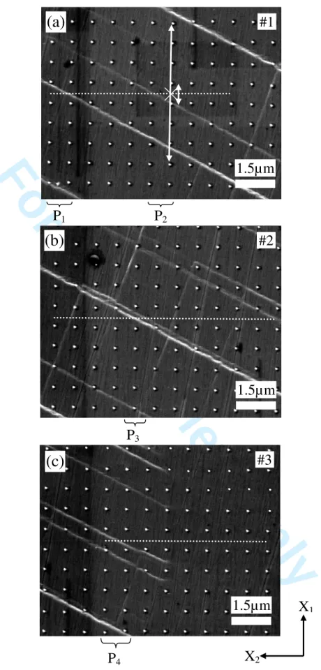
On the other hand, the evolution of ε11 calculated using a gauge length of 0.73 µm revealed the presence of four main peaks defined by high strain intensities (peak P1 at 0.73 µm and 8.9 %, peak P2 at 3.65 µm and 5.1 %, peak P3 at 10.20 µm and 15.7 % and peak P4 at 15.30 µm and 7.0 % in Fig. 11(c)) and corresponding to the presence of a large slip band at the position of measurement (P1 and P2 in Fig. 12(a), P3 in Fig. 12(b) and P4 in Fig. 12(c)). In addition, the strain evolution was well resolved at the interface where the strain was found to change continuously (1.2 % on both sides).
Evolution of ε11 along the X1-axis. By contrast to the measurements performed in the absence
of large slip bands, significant fluctuations of ε11 were also measured along the X1-axis within highly plastically deformed grains, as shown in Figs. 11(d) and (e). These fluctuations were 3 4 5 6 7 8 9 10 11 12 13 14 15 16 17 18 19 20 21 22 23 24 25 26 27 28 29 30 31 32 33 34 35 36 37 38 39 40 41 42 43 44 45 46 47 48 49 50 51 52 53 54 55 56 57 58 59 60
For Peer Review Only
mainly observed within the austenite where a higher density of slip bands was found to emerge. For example, four sharp peaks were identified in Fig. 11(e) at 12.43 µm, 17.54 µm (peak P5), 19.00 µm (peak P6) and 21.2 µm (peak P7). Surface observations at high resolution confirmed that these peaks are systematically related to the emergence of large slip bands, as shown in Fig. 13.
Evolution of ε22 along the X1- and X2-axis. As in the previous case, no large fluctuations of ε22 were detected along the two directions using the different gauge lengths, as shown in Figs. 14. This demonstrates that large slip bands have almost no effects on the values of this strain component. For example, the large slip band P3 visible in Fig. 12(b) induces nearly no changes in the value of ε22 (Fig. 14(b)) whereas the value of ε11 was found to increase up to about 15 % (Fig. 11(c)).
3.5 Discussion
Recently, computational methods based on the continuum theory of dislocations have been developed to calculate the stress field due to specified dislocation distribution [17] and residual stresses in expitaxial layers [18]. In the former case, the tensor maps of dislocation distribution were extracted by digital processing of HRTEM images and used as the input data to the finite-element code. Other models [19] ascribed size effects ocurring during plastic deformation on thin films to the bowing and glide of continuously distributed dislocations. They also showed the dependence of the stress on the grain orientation and the stress saturation. The authors pointed out that a quantitative agreement was found between the numerical results obtained from this model and experimental data [20] derived from uniaxial tensile tests on unpassivated, polycrystalline Cu-films with thicknesses ranging from 0.4 to 3 4 5 6 7 8 9 10 11 12 13 14 15 16 17 18 19 20 21 22 23 24 25 26 27 28 29 30 31 32 33 34 35 36 37 38 39 40 41 42 43 44 45 46 47 48 49 50 51 52 53 54 55 56 57 58 59
For Peer Review Only
Lithography at the nanoscale may be very useful to validate numerical results obtained from the computational methods described previously. It will also be possible to determine the influence of dislocations pile-ups on the surface mechanical properties of metallic alloys and semiconductors under straining conditions (after fatigue and monotonic tests, etc.) and to investigate the role of surface layers on the mechanisms of emergence of dislocations. In addition, experimental results obtained at the micro- and submicroscale by means of lithography may be compared to numerical simulation based on nonlinear finite-element methods and molecular dynamics.
Lithography also opens a wide field of investigations regarding the influence of surface treatments on the mechanical behaviour of metallic alloys and their reactivity in the presence of an aggressive environment. Strain gradients revealed at the microscale (and mainly the variations of ε11) are key parameters to better understand the reactivity of metallic alloys and to predict their lifetime in aggressive environments, by taking into account the specimen microstructure and the surface strain field in the analysis of electrochemical results derived from local investigations by means of the scanning vibrating electrode technique and microcapillary-based techniques.
4. Conclusion
The use of grid points fabricated at the microscale through the electron beam lithography process has allowed high resolution mapping of strain gradients at the stainless steel surface (gauge length as small as 0.73 µm). Significant differences in the mechanical behaviour of both phases were then observed. Considering the strain in the loading direction, the austenite was found to undergo 6 % plastic strain in average for an applied strain of 4.6 %. 3 4 5 6 7 8 9 10 11 12 13 14 15 16 17 18 19 20 21 22 23 24 25 26 27 28 29 30 31 32 33 34 35 36 37 38 39 40 41 42 43 44 45 46 47 48 49 50 51 52 53 54 55 56 57 58 59 60
For Peer Review Only
In addition, a highly heterogeneous strain distribution which was controlled by the morphology and density of slip bands was found in this phase. It was observed that extremely small slip bands generally induced smooth strain variations whereas large slip bands caused sharp increases of the local strain (and therefore high strain gradients). The ferrite was less in tension (3.7 % plastic strain in average) than the austenite and strain gradients were only detected close to the interface (the strain field was more-or-less uniform far from the interface) to accommodate with the austenite strain state. Combined with the atomic force microscopy (AFM), this method may provide quantitative information on the role of the dislocations density on the surface strain field.
Acknowledgments
The authors are grateful to Commissariat à l’Energie Atomique-Direction des Réacteurs Nucléaires (CEA-DRN)/Département de Mécanique de la Technologie (DMT)/SEMT (Saclay, France) which has designed and developed the FE code Cast3M. The authors are also grateful to J. Peultier (Industeel, Arcelor group) for providing specimens. One of the author (D.K.) would like to thank the Conseil Régional de Bourgogne (France) for financial support. In the present study, the authors from the LPUB (J.C.W. and E.F.) prepared the lithography. 3 4 5 6 7 8 9 10 11 12 13 14 15 16 17 18 19 20 21 22 23 24 25 26 27 28 29 30 31 32 33 34 35 36 37 38 39 40 41 42 43 44 45 46 47 48 49 50 51 52 53 54 55 56 57 58 59
For Peer Review Only
References
[1] J. Man, K. Obrtlik, J. Polak, Mater. Sci. and Eng. A. 351 123 (2003). [2] J. Polak, J. Man and K. Obrtlik, Int. J. of Fatigue 25 1027 (2003).
[3] D. Chandrasekaran and M. Nygards, Mat. Sci. and Eng. A 365 191 (2004). [4] M. Hayakawa, S. Matsuoka and Y. Furuya, Mat. Lett., 57 3037 (2003). [5] D. Chandrasekaran and M. Nygards, Acta. Mat. 51 5375 (2003). [6] D.P. Field, Ultramicroscopy 67 1 (1997).
[7] B.L. Adams, Ultramicroscopy 67 11 (1997). [8] D.J. Jensen, Ultramicroscopy 67 25 (1997).
[9] E.A. Franke, D.J. Wenzel and D.L.Davidson, Rev. of Sci. Instr. 62 1270 (1991). [10] J. Kang, D.S. Wilkinson, M. Jain et al., Acta Materialia 54 209 (2006).
[11] J. Kang, M. Jain, D.S. Wilkinson, J.D. Embury, J Strain Anal Eng Des 40 559 (2005). [12] R.A. Carolan, M. Egashira, S. Kishimoto et al., Acta Metall. Mater. 40 1629 (1992). [13] Y.L. Liu and G. Fisher, Scripta Mat. 36 1187 (1997).
[14] L. Allais, M. Bornert, D. Bretheau et al., Acta Metall. Mater. 42 3865 (1994). [15] E. Soppa, P. Doumalin, P. Binkele et al., Comput. Mat. Sci. 21 261 (2001). [16] V. Vignal, E. Finot, R. Oltra et al., Ultramicroscopy 103 189 (2005). [17] G. Maciejewski, P. Dluzewski, Comput. Mat. Sci. 30 44 (2004). [18] P. Dluzewski, G. Maciejewski, Comput. Mat. Sci. 29 379 (2004).
[19] C. Schwarz, R. Sedlacek, E. Werner, Mater. Sci. Eng. A 400-401 443 (2005). [20] M. Hommel, O. Kraft, Acta Mater. 49 3935 (2001).
3 4 5 6 7 8 9 10 11 12 13 14 15 16 17 18 19 20 21 22 23 24 25 26 27 28 29 30 31 32 33 34 35 36 37 38 39 40 41 42 43 44 45 46 47 48 49 50 51 52 53 54 55 56 57 58 59 60
For Peer Review Only
Caption
Fig. 1. (a) Lamellar and (b) globular microstructures of the duplex stainless steel.
Fig. 2. (a) Morphology of tensile specimens used in the experiments (the stress is applied along the X1-axis). (b) Schematic representation of the 20 patterns deposited on the gauge surface of tensile specimens and (c) FE-SEM image of pads in a pattern.
Fig. 3. Stress field around a nickel pad calculated for an applied stress of 360 MPa (roughly 4.6% plastic strain).
Fig. 4. (a-c) FE-SEM micrographs of the specimen surface where measurements shown in Fig. 5 were performed. X1 is the loading direction. The lines A-B and A’-B’ represent different gauge lengths and SB1 represents a large slip band in (b).
Fig. 5. (a-c) Distribution of ε11 vs. the position of measurement from the point A to the point B reported in Fig. 4(a-c), respectively, using a gauge length of 0.73 µm. (d) Evolution of ε11 along the slip band SB1 shown in Fig. 4 (b) from the point C to the point D. Evolution of ε11 vs. the gauge length : (e-g) experimental values determined within the sites shown in Fig. 4(a-c), respectively and (h-j) numerical values calculated from Equation (3).
Fig. 6. (a-b) Evolution of the in-plane strain components ε11 and ε22 determined at the microscale (gauge length : 5.11 µm) within several grains of both phases on the strained specimen (4.6% plastic strain).
3 4 5 6 7 8 9 10 11 12 13 14 15 16 17 18 19 20 21 22 23 24 25 26 27 28 29 30 31 32 33 34 35 36 37 38 39 40 41 42 43 44 45 46 47 48 49 50 51 52 53 54 55 56 57 58 59
For Peer Review Only
Fig. 7. (a) Dark field optical image and (b) optical image of the grain #2 reported in Fig. 6. (c) optical image of the grain #8 reported in Fig. 6 and (d) Dark field optical image of the grain #4 reported in Fig. 6. The mechanical analysis was performed within the regions delimited by the circles. X1 is the loading direction.
Fig. 8. (a) FE-SEM micrograph of the microstructure where the mechanical analysis was performed along the two dotted lines. Evolution of ε11 (b-c) along the X2-axis for a gauge length of 5.11 µm and 0.73 µm, respectively, and (d-e) along the X1-axis for a gauge length of 5.11 µm and 0.73 µm, respectively. X1 is the loading direction.
Fig. 9. (a-c) FE-SEM micrographs at high magnification of the microstructure and slip bands within the images # 1, #3 and #5 along the X2-axis reported in Fig. 8 (austenite grain : images #1 and #3, ferrite grain : image #5). X1 is the loading direction.
Fig. 10. (a) FE-SEM micrograph of the microstructure where the mechanical analysis was performed along the two dotted lines. Evolution of ε22 (b-c) along the X2-axis for a gauge length of 5.11 µm and 0.73 µm, respectively, and (d-e) along the X1-axis for a gauge length of 5.11 µm and 0.73 µm, respectively. X1 is the loading direction.
Fig. 11. (a) FE-SEM image of the microstructure where the mechanical analysis was performed along the two dotted lines. Evolution of ε11 (b-c) along the X2-axis for a gauge length of 5.11 µm and 0.73 µm, respectively, and (d-e) along the X1-axis for a gauge length of 5.11 µm and 0.73 µm, respectively. X1 is the loading direction.
3 4 5 6 7 8 9 10 11 12 13 14 15 16 17 18 19 20 21 22 23 24 25 26 27 28 29 30 31 32 33 34 35 36 37 38 39 40 41 42 43 44 45 46 47 48 49 50 51 52 53 54 55 56 57 58 59 60
For Peer Review Only
Fig. 12. (a-c) FE-SEM micrographs at high magnification of the microstructure and slip bands within the images # 1, #2 and #3 along the X2-axis reported in Fig. 11 (austenite grain : images #1 and #2, interface : image #3). X1 is the loading direction.
Fig. 13. FE-SEM micrograph at high magnification of the microstructure and slip bands within the image #5 along the X2-axis reported in Fig. 11 (austenite grain). X1 is the loading direction.
Fig. 14. Evolution of ε22 (a-b) along the X2-axis for a gauge length of 5.11 µm and 0.73 µm, respectively, and (c-d) along the X1-axis for a gauge length of 5.11 µm and 0.73 µm, respectively. X1 is the loading direction.
3 4 5 6 7 8 9 10 11 12 13 14 15 16 17 18 19 20 21 22 23 24 25 26 27 28 29 30 31 32 33 34 35 36 37 38 39 40 41 42 43 44 45 46 47 48 49 50 51 52 53 54 55 56 57 58 59
For Peer Review Only
50 µm
X
1(rolling direction)
X
2X
3(a)
X1 (Rolling direction) X2 X3(b)
100 µm 3 4 5 6 7 8 9 10 11 12 13 14 15 16 17 18 19 20 21 22 23 24 25 26 27 28 29 30 31 32 33 34 35 36 37 38 39 40 41 42 43 44 45 46 47 48 49 50 51 52 53 54 55 56 57 58 59 60For Peer Review Only
1 µm
(c)
X
2X
1Pattern 1
Pattern 2
(b)
X
2X
1(75×75 µm
2)
(a)
X
2X
1 3 4 5 6 7 8 9 10 11 12 13 14 15 16 17 18 19 20 21 22 23 24 25 26 27 28 29 30 31 32 33 34 35 36 37 38 39 40 41 42 43 44 45 46 47 48 49 50 51 52 53 54 55 56 57 58 59For Peer Review Only
340 MPa
500 MPa
σ
11X
1X
3(loading direction)
3 4 5 6 7 8 9 10 11 12 13 14 15 16 17 18 19 20 21 22 23 24 25 26 27 28 29 30 31 32 33 34 35 36 37 38 39 40 41 42 43 44 45 46 47 48 49 50 51 52 53 54 55 56 57 58 59 60For Peer Review Only
X
1B’
A’
B
A
4 , 11ε
3 , 11ε
2 , 11ε
1 , 11ε
* 2 , 11ε
* 3 , 11ε
* 4 , 11ε
B
1.5µm
(a)
A
B
A’
B’
X
2(c)
1.5µm
A
B
A’
B’
(b)
B
1.5µm
A
A’
B’
SB1
C
D
2 3 4 3 4 5 6 7 8 9 10 11 12 13 14 15 16 17 18 19 20 21 22 23 24 25 26 27 28 29 30 31 32 33 34 35 36 37 38 39 40 41 42 43 44 45 46 47 48 49 50 51 52 53 54 55 56 57 58 59For Peer Review Only
0 0 1 2 3 4 5 5 10 15 20 B A (a) (b) (c) ε 11 ( % )Position of measure (path along X1, µm)
0 2 4 6 0 5 10 15 20 (e) (f) (g) (h) (i) (j) ε1 1 ( % ) Gauge length (µm) 0 2 4 6 8 5 10 15 20 D C (d) ε11 (% )
Position of measure (along a slip band, µm)
3 4 5 6 7 8 9 10 11 12 13 14 15 16 17 18 19 20 21 22 23 24 25 26 27 28 29 30 31 32 33 34 35 36 37 38 39 40 41 42 43 44 45 46 47 48 49 50 51 52 53 54 55 56 57 58 59 60
For Peer Review Only
0 2 4 6 8 10 12 14 16 18 20 -6 -3 0 3 6 ε 2 2 (% ) Grain label 0 2 4 6 8 10 12 14 16 18 20 0 2 4 6 8 10 123.7%
austenite ferrite ε 1 1 (% ) Grain label4.8%
6.0%
S
1S
2S
3S
6, S
7, S
8 (a) (b)S
1S
4S
2S
3S
5 3 4 5 6 7 8 9 10 11 12 13 14 15 16 17 18 19 20 21 22 23 24 25 26 27 28 29 30 31 32 33 34 35 36 37 38 39 40 41 42 43 44 45 46 47 48 49 50 51 52 53 54 55 56 57 58 59For Peer Review Only
(b)
20 µm
S
2S
1S
3 grain #2 S8 S6 S7(b)
20 µm S1 S2 S3(a)
20 µmS
5S
4(c)
20 µm
X
1X
2 grain #8 (d) (a) 3 4 5 6 7 8 9 10 11 12 13 14 15 16 17 18 19 20 21 22 23 24 25 26 27 28 29 30 31 32 33 34 35 36 37 38 39 40 41 42 43 44 45 46 47 48 49 50 51 52 53 54 55 56 57 58 59 60For Peer Review Only
1
2
3
4
5
20µm
(a)
ferrite austeniteX
1X
21 2 3 4 5 6
0 5 10 15 20 25 30 0 2 4 6 8 (e) ε11 (% )Position of measure (path along X1, µm)
0 5 10 15 20 25 30 0 2 4 6 8 5 4 3 2 1 (d) austenite ferrite ε 11 (% )
Position of measure (path along X1, µm)
0 1 0 2 0 3 0 4 0 5 0 0 2 4 6 8 (b ) 6 5 4 3 2 1 a u ste n ite fe rrite ε11 (% ) P o sitio n o f m e a su re (p a th a lo n g X2, µ m ) 0 10 20 30 40 50 0 2 4 6 8 (c) P1 ε11 (% )
Position of measure (path along X2, µm) 3 4 5 6 7 8 9 10 11 12 13 14 15 16 17 18 19 20 21 22 23 24 25 26 27 28 29 30 31 32 33 34 35 36 37 38 39 40 41 42 43 44 45 46 47 48 49 50 51 52 53 54 55 56 57 58 59
For Peer Review Only
X
2X
1(c)
1.5µm
#5
1.5µm
(a)
#1
(b)
1.5µm
#3
P
1 3 4 5 6 7 8 9 10 11 12 13 14 15 16 17 18 19 20 21 22 23 24 25 26 27 28 29 30 31 32 33 34 35 36 37 38 39 40 41 42 43 44 45 46 47 48 49 50 51 52 53 54 55 56 57 58 59 60For Peer Review Only
0 10 20 30 40 50 -8 -6 -4 -2 0 (c) ε22 (% )Position of measure (path along X2, µm)
0 10 20 30 40 50 -8 -6 -4 -2 0 austenite ferrite 6 5 4 3 2 1 (b) ε22 (% )
Position of measure (path along X2, µm)
1
2
3
4
5
20µm
(a)
ferrite austeniteX
1X
21 2 3 4 5 6
0 5 10 15 20 25 30 -8 -6 -4 -2 0 5 4 3 2 1 (d) austenite ferrite ε22 ( % )Position of measure (path along X1, µm)
0 5 10 15 20 25 30 -8 -6 -4 -2 0 (e) ε22 (% )
Position of measure (path along X1, µm) 3 4 5 6 7 8 9 10 11 12 13 14 15 16 17 18 19 20 21 22 23 24 25 26 27 28 29 30 31 32 33 34 35 36 37 38 39 40 41 42 43 44 45 46 47 48 49 50 51 52 53 54 55 56 57 58 59
For Peer Review Only
0 5 10 15 20 25 30 35 0 2 4 6 8 5 (b) 4 3 2 1 ε11 (%)Position of measure (path along X2, µm) austenite ferrite 0 5 10 15 20 25 30 35 0 5 10 15 20 P3 P4 P2 P1 (c) ε11 (%)
Position of measure (path along X2, µm) X1 X2 austenite ferrite 10µm
(a)
1 2 3 4 5 6 1 2 3 4 5 0 5 10 15 20 25 30 0 5 10 15 20 (e) P7 P6 P5 ε11 (% )Position of measure (path along X1, µm)
0 5 10 15 20 25 30 0 2 4 6 8 (d) 6 5 4 3 2 1 ε11 (%)
Position of measure (path along X1, µm)
3 4 5 6 7 8 9 10 11 12 13 14 15 16 17 18 19 20 21 22 23 24 25 26 27 28 29 30 31 32 33 34 35 36 37 38 39 40 41 42 43 44 45 46 47 48 49 50 51 52 53 54 55 56
For Peer Review Only
(b)
1.5µm
#2
P
3X
1X
2(c)
1.5µm
#3
P
41.5µm
(a)
#1
P
1P
2 3 4 5 6 7 8 9 10 11 12 13 14 15 16 17 18 19 20 21 22 23 24 25 26 27 28 29 30 31 32 33 34 35 36 37 38 39 40 41 42 43 44 45 46 47 48 49 50 51 52 53 54 55 56 57 58 59For Peer Review Only
#5
1.5µm
P
5P
6P
7 3 4 5 6 7 8 9 10 11 12 13 14 15 16 17 18 19 20 21 22 23 24 25 26 27 28 29 30 31 32 33 34 35 36 37 38 39 40 41 42 43 44 45 46 47 48 49 50 51 52 53 54 55 56 57 58 59 60For Peer Review Only
0 5 10 15 20 25 30 -10 -8 -6 -4 -2 0 6 5 4 3 2 1 ferrite austenite ε22 (% )Position of measure (path along X1 , µm)
(c) 0 5 10 15 20 25 30 -10 -8 -6 -4 -2 0 ε22 (% )
Position of measure (path along X1, µm)
0 5 10 15 20 25 30 35 -10 -8 -6 -4 -2 0 P 3 ε22 (% )
Position of measure (path along X2, µm)
(b) 0 5 10 15 20 25 30 35 -10 -8 -6 -4 -2 0 ferrite austenite 5 4 3 2 1 ε22 (% )
Position of measure (path along X2, µm)
(a) (d) 3 4 5 6 7 8 9 10 11 12 13 14 15 16 17 18 19 20 21 22 23 24 25 26 27 28 29 30 31 32 33 34 35 36 37 38 39 40 41 42 43 44 45 46 47 48 49 50 51 52 53 54 55 56 57 58 59
For Peer Review Only
High spatial resolution strain measurements
at the surface of duplex stainless steels
D. Kempf1, V. Vignal1,*, G. Cailletaud2, R. Oltra1, J.C. Weeber3, and E. Finot3
1 LRRS, UMR 5613 CNRS – Université de Bourgogne, BP 47870, 21078 Dijon, France
2 Centre des Matériaux, UMR 7633 CNRS – Ecole des Mines de Paris, BP 87, 91003 Evry, France
3 LPUB, UMR 5027 CNRS – Université de Bourgogne, BP 47870, 21078 Dijon, France
Abstract
The determination of local strain fields at the surface of materials is of major importance for understanding their reactivity. In the present paper, lithography is used to fabricate grid points at the microscale and to map strain gradients within grains and between grains. This method was applied to duplex stainless steels which exhibit heterogeneous strain distributions under straining conditions. The influence of various parameters (the specimen microstructure, the density of slip bands, the number of systems activated and the grid geometry) on the strain value was discussed.
Keywords : local extensometry, strain, duplex stainless steel, microstructure
3 4 5 6 7 8 9 10 11 12 13 14 15 16 17 18 19 20 21 22 23 24 25 26 27 28 29 30 31 32 33 34 35 36 37 38 39 40 41 42 43 44 45 46 47 48 49 50 51 52 53 54 55 56 57 58 59 60
For Peer Review Only
1. Introduction
Duplex stainless steels are highly important engineering materials, due to their generally high corrosion resistance and their high strength and toughness. They have a complex microstructure with comparable volume of austenite and ferrite. Due to differences in mechanical properties, a heterogeneous strain distribution is generated in both phases under straining conditions and the presence of these surface strain gradients may affect the physico-chemical properties of the material. Therefore, it is of major importance to quantify surface strains at the microstructure scale.
Atomic force microscopy (AFM) offers the possibility to examine the 3D surface morphology in order to evaluate in-plane changes (up to 150 × 150 µm2) and to measure out-of-plane differences (up to 6 µm) at the microscale. AFM has been used to study the surface topography of fatigued stainless steels, especially in kinetic study of growth where the shape of extrusions and intrusions has been followed as a function of the number of loading cycles [1-2]. Description of plastic deformation processes and strain gradients around grain boundaries has also been proposed after uniaxial tensile loading [3-4]. These studies remain qualitative and only a few parameters, such as the surface roughness and the steps height, have been determined as a function of applied strain. However, combining AFM with the electron back-scatter diffraction (EBSD) has permitted to show that the surface roughness and the misorientation of grains increase linearly with increasing applied strain [5-8].
Regarding quantitative approaches, a stereoimaging technique (including a Cognex 2000 image processing system, cameras to obtain digital images from analog photographs, a graphics display terminal, a track ball for operator interaction with the system and a video 3 4 5 6 7 8 9 10 11 12 13 14 15 16 17 18 19 20 21 22 23 24 25 26 27 28 29 30 31 32 33 34 35 36 37 38 39 40 41 42 43 44 45 46 47 48 49 50 51 52 53 54 55 56 57 58 59
For Peer Review Only
measurements of microdisplacements under high resolution conditions [9]. Microscopic strain mapping using SEM topography image correlation at large strain was also performed on aluminum alloys and relationships between slip lines, dynamic strain aging, shear localization, diffuse and localized necking were obtained [10-11]. In addition, object grating methods have been proposed for evaluating local strains in multiphase or composite materials in which the microstructural scale is in the order of tens micrometers and at microstructural inhomogeneities such as grain boundaries and crack tips. However, all the authors have claimed that the complexity of the experimental strain distribution is better explained by the complementary use of a finite element model. The effect of grain boundary deformation on the creep micro-deformation of pure copper [12], the influence of the presence of A1203 particles in aluminium alloys [13] and the behaviour of iron/silver and iron/copper blends [14] have been studied under uniaxial tensile stress. On the other hand, composite Ag-Ni materials have been tested under uniaxial compression [15].
A similar technique has been applied to duplex stainless steels at the mesoscale with a gauge length of about 50 µm [16]. The strain in the loading direction was found to vary significantly from one grain to another, and inside grains, from 2.2 % to 6.2 % for an applied strain of 4.5 %. By contrast, the strain in the direction perpendicular to loading was smaller and remained more-or-less constant over a large number of grains (compression of about -1.3 %). This was attributed to the fact that swelling of grains in this direction was restricted by the constraints imposed by neighbouring grains. It has also been shown that the surface roughness increases linearly with the out-of-plane strain component. In the present paper, surface strains were mapped at the microscale on duplex stainless steels and the role of the microstructure on the existence of microstrain gradients was discussed. This implied the development of grids with a high spatial resolution and sharp precision. The influence of the grid geometry (size of 3 4 5 6 7 8 9 10 11 12 13 14 15 16 17 18 19 20 21 22 23 24 25 26 27 28 29 30 31 32 33 34 35 36 37 38 39 40 41 42 43 44 45 46 47 48 49 50 51 52 53 54 55 56 57 58 59 60
For Peer Review Only
pads, distance between two successive pads, gauge length, etc.), on the strain value was also discussed. In addition, the proposed method has revealed the strain heterogeneities induced by the emergence of slip bands and has allowed an experimental quantification of the activity of these systems in both metallic phases.
2. Experimental
2.1. Tensile specimens and surface preparation
Experiments were performed on a duplex stainless steel (UNS S31803, chemical composition : C : 0.02wt.%; Mn : 1.62%; Ni : 5.45%; Cr : 22.44%; Mo : 2.92%; N : 0.17% and Si : 0.39%). It was hot rolled to obtain 20 mm thick sheets, solution annealed at 1050°C for 15 min and water quenched. Specimens showed a lamellar microstructure with a grain size of about 5 µm in the lamellar direction, as shown in Fig. 1(a). In order to increase the grain size, a second heat treatment was carried out consisting of a homogenization treatment at 1300°C for 1 hour, followed by a slow cooling down to 1080°C (formation of the austenite) and a water quenching. The volume fraction of austenite and ferrite was evaluated to 50/50 and the grain size was about 75 µm, as shown in Fig. 1(b). The 0.2% yield strength (Rp0.2) and the ultimate strength (Rm) of this material were 560 and 760 MPa at 25°C, respectively.
Tensile specimens were machined in order to have a cross-section of 2 × 6 mm2 and a gauge length of 25 mm, as shown in Fig. 2(a). They were mechanically ground using emery papers and polished using diamond pastes (down to 1 µm). The average surface roughness was then evaluated to about 5 nm (calculated on 50 × 50 µm2 areas).
2.2. Elaboration of the grid points
3 4 5 6 7 8 9 10 11 12 13 14 15 16 17 18 19 20 21 22 23 24 25 26 27 28 29 30 31 32 33 34 35 36 37 38 39 40 41 42 43 44 45 46 47 48 49 50 51 52 53 54 55 56 57 58 59
For Peer Review Only
A conventional process of electron beam lithography was used as described in Ref [16]. A 300 nm depth resin film (PMMA) was spin coated on the gauge surface of tensile specimens before being baked for 3 hours at 175 °C in order to become stiff. An electron beam microscope was used to mark the surface by local chemical damages in the resin layer. The electron beam microscope was a Jeol 6500F and was coupled with a beam position controller software (Raith Elphy Quantum). Chemically modified zones of the layer were attacked preferentially in a first solvent solution for a few seconds with ultrasonic waves. Then, this development stage was stopped in second solvent bath with ultrasonic waves and the tensile specimens were then blown dry with pure nitrogen. A first layer of about 50 nm nickel was then deposited in an electron gun evaporator and recovered in a thermal evaporator by a second layer of 10 nm gold. Nickel was chosen because of its good adherence on metallic substrates and the thin layer of gold was deposited in order to locate easily the 20 arrays of pads on the gauge surface from optical observations, as schemed in Fig. 2(b). The last stage consists of a lift-off : the remaining resin was removed and the metallic (Ni and Au) pads became apparent. Finally, the sample was blown dry with pure nitrogen.
2.3. Mechanical tests and surface observations at the microscale
Tensile specimens were then subjected to uniaxial tensile loading in air at 4.6% plastic strain applied along the X1-axis using a home-made tensile microstage. Surface observations were performed after unloading using a field-emission type scanning electron microscope (FE-SEM, JEOL 6400F).
3. Results and discussion
The in-plane strain components were evaluated from the average distance between centroids of pads using the genuine strain-displacement relationships :
3 4 5 6 7 8 9 10 11 12 13 14 15 16 17 18 19 20 21 22 23 24 25 26 27 28 29 30 31 32 33 34 35 36 37 38 39 40 41 42 43 44 45 46 47 48 49 50 51 52 53 54 55 56 57 58 59 60
For Peer Review Only
L L L 0 , 1 0 , 1 1 11 −−−− ==== ε , L L L 0 , 2 0 , 2 2 22 −−−− ==== ε (1)where L1 and L2 are the average distances between centroids of pads along the X1- and X2 -axis, respectively, after deformation and L1,0 and L2,0 are the average distances before deformation. The distance between centroids of pads was measured from section profiles (obtained from FE-SEM images) which were smoothed using a lowpass frequency filter (f > 1 Hz). When a pad was located straight above a slip band, peeling may occur and therefore no strain measurement was carried out.
3.1. Characteristics of the grid points and high spatial resolution strain measurements
Mapping microstress gradients within grains and across the austenite/ferrite interface on the globular microstructure shown in Fig. 1(b) requires the use of specific grids. In this case, the gauge length must be smaller than 10 µm (to have several values within a grain) and the distance between two points of measurement must be smaller than 1 µm (to have a good spatial period for computation). In order to optimize these parameters, the influence of pads on the surface stress field was investigated under straining conditions by means of numerical simulation. The substrate was assumed to be pure austenite having an isotropic elastic-plastic behaviour (the elastic-plastic material model used was determined by fitting experimental stress-strain curves obtained until the ultimate stress with the finite element method model). On the other hand, pads were assumed to be pure nickel having an elastic behaviour (the surface stress around pads is then slightly overestimated). QUAD4 elements composed of four nodes located at the four geometric corners of quadrangles were used in the meshing and the density of elements was chosen such that each pad was composed of 35×35 elements. To prevent undesirable edge effects, the substrate thickness was ten times larger than the 3 4 5 6 7 8 9 10 11 12 13 14 15 16 17 18 19 20 21 22 23 24 25 26 27 28 29 30 31 32 33 34 35 36 37 38 39 40 41 42 43 44 45 46 47 48 49 50 51 52 53 54 55 56 57 58 59
For Peer Review Only
The loading (360 MPa, corresponding roughly to 4.6 % plastic strain) was applied to the left edge of the region analysed. Significant stress concentrations were observed around pads and these gradients extend over a distance of about twice the diameter of pads, as shown in Fig. 3. Therefore, in order to prevent interactions between pads that would affect the results, the ratio of the distance between pads to the diameter of pads must be chosen at least equal to 4.
Considering these limitations (gauge length smaller than 10 µm and ratio of the distance between pads to the diameter of pads greater than 4), the diameter and the height of pads were fixed to 70 nm and the distance between pads was set at 730 nm in the two directions. Numerous surface observations on the unstrained specimens showed that the fabrication process induced a dispersion of ± 4.5 nm on the distance between pads. As the size of these pads was of the same order of magnitude as the radius of curvature at the tip apex, AFM images revealed distorted pads from which no accurate measurements could be performed. The mechanical analysis was then carried out from FE-SEM images recorded at a magnification of 14,000 (8.59×6.87 µm2), as shown in Fig. 2(c). At this resolution, the pixel size was 6.7 nm for an image size of 1280×1024 pixels.
It has to be pointed out that the error made on the determination of the pad position was estimated to ±1 pixel. The relative errors in percentage of the exact value of strain were estimated from Equation (2) to about ±1.84 % and ±0.26 % for a gauge length of 0.73 µm and 5.11 µm, respectively. 100 ) ( _ ) ( _ ) ( _ 2 (%) = ± × × µm length gauge µm size image px resolution image error (2)
The resolution in strain can be significantly improved by measuring the average distance between pads on numerous section profiles determined on a large scale. In this case, no 3 4 5 6 7 8 9 10 11 12 13 14 15 16 17 18 19 20 21 22 23 24 25 26 27 28 29 30 31 32 33 34 35 36 37 38 39 40 41 42 43 44 45 46 47 48 49 50 51 52 53 54 55 56 57 58 59 60
For Peer Review Only
value of strain was decreased down to about ±4.5/(8×730) = 0.08 %. Therefore, the method proposed is suitable for mapping plastic strains at the microscale (above 15 % plastic strain, the surface roughness becomes too high and cannot be neglected in the strain calculation [14]) and for quantifying elastic strains at the mesoscale.
3.2. Strain field around a slip band and effects of the gauge length on the strain value
In order to map the strain field around slip bands in the loading direction, several values of ε11 were measured along straight lines, from the point A to the point B in Fig. 4, using a gauge length of 0.73 µm (the strain was measured between two successive pads). In the absence of any visible slip bands crossing the line A-B, ε11 was found to be constant. In the case of Fig. 4(a), a value of about 3 % was derived from the calculation, as shown in Fig. 5(a). By contrast, a sharp increase of ε11 was observed straight above slip bands, as shown in Figs. 4(b)-(c) and 5(b)-(c), indicating that the strain concentration induced by these line defects extends over a very short distance. Therefore, quantifying the strain field around surface defects (such as slip bands, grain boundaries and interfaces between metallic phases) requires the use of high spatial resolution methods. It can also be noticed that the larger the slip band, the higher the maximum strain value reached (of about 8.9 % in Fig. 5(b) for the small slip band visible in Fig. 4(b) and 15.2 % in Fig. 5(c) for the large slip band visible in Fig. 4(c)) and that the highest strain value obtained was about three times greater than the applied strain (of about 4.6 %).
It is also interesting to note that ε11 may not be constant along a slip band. The value of ε11 was found to vary along the slip band SB1 reported in Fig. 4(b) from 8 % plastic strain at the point C up to about 13 % at the point D whereas the distance between the two points 3 4 5 6 7 8 9 10 11 12 13 14 15 16 17 18 19 20 21 22 23 24 25 26 27 28 29 30 31 32 33 34 35 36 37 38 39 40 41 42 43 44 45 46 47 48 49 50 51 52 53 54 55 56 57 58 59
For Peer Review Only
was around 8 µm as shown in Fig. 5(d). This indicates that high strain gradients may exist along such line defects (of about 0.6 %/µm in average for the slip band SB1).
The influence of the gauge length on the strain value was then studied within the three same sites in order to determine the pertinent scale of analysis and to correlate the results to physically meaningful quantities. The gauge length varied from 5.11 µm (distance between the points A and B in Fig. 4 including seven intervals between pads) down to 0.73 µm (distance between the points A’ and B’ in Fig. 4 including one interval between pads) while the position of measurement was maintained unchanged (corresponding to the cross in Fig. 4). The strain measured over a distance including several intervals between pads, ( )(%)
11
N
ε , was equal to the average of the strains determined on each interval (with a gauge length of 0.73 µm) :
(
)
+ + = =∑
+ = = = = = 2 / ) 1 ( 2 ) 1 ( , 11 ) 1 ( , 11 ) 1 ( 1 , 11 ) ( 11 ) 1 ( 1 , 11 ) 1 ( 11 * 1 (%) (%) N i N i N i N N N N ε ε ε ε ε ε (3)where N (= 3, 5 or 7) is the number of intervals between pads considered (the gauge length is then given by N×0.73 (µm)), ( 1)(%) , 11 = N i ε and *( 1)(%) , 11 = N i
ε are the strains measured on both sides
of the slip band with a gauge length of 0.73 µm (see the scheme insert in Fig. 4). Fig. 5 (e)-(j) shows that the strains measured for different gauge lengths are in an excellent agreement with the strains calculated using Equation (3), indicating that the method proposed gives accurate results for a wide range of gauge lengths. Furthermore, this indicates that the error made using a 0.73 µm gauge length was significantly lower than the value determined from Equation (2). This error was at least as small as the error calculated for a gauge length of 5.1 µm (of about 0.26%). For gauge lengths above 3.65 µm, the strain was constant, as shown in Fig. 5 (e)-(j), and such measurements were very useful to obtain information about the average strain state 3 4 5 6 7 8 9 10 11 12 13 14 15 16 17 18 19 20 21 22 23 24 25 26 27 28 29 30 31 32 33 34 35 36 37 38 39 40 41 42 43 44 45 46 47 48 49 50 51 52 53 54 55 56 57 58 59 60