HAL Id: hal-01166475
https://hal.archives-ouvertes.fr/hal-01166475
Submitted on 23 Jun 2015
HAL is a multi-disciplinary open access
archive for the deposit and dissemination of
sci-entific research documents, whether they are
pub-lished or not. The documents may come from
L’archive ouverte pluridisciplinaire HAL, est
destinée au dépôt et à la diffusion de documents
scientifiques de niveau recherche, publiés ou non,
émanant des établissements d’enseignement et de
Optical absorption and thermal conductivity of GaAsPN
absorbers grown on GaP in view of their use in
multijunction solar cells
S. Ilahi, Samy Almosni, Fares Chouchane, Mathieu Perrin, K. Zelazna, N.
Yacoubi, R. Kudrawiec, Pierre Râle, Laurent Lombez, Jean-François
Guillemoles, et al.
To cite this version:
S. Ilahi, Samy Almosni, Fares Chouchane, Mathieu Perrin, K. Zelazna, et al..
Optical
absorp-tion and thermal conductivity of GaAsPN absorbers grown on GaP in view of their use in
mul-tijunction solar cells.
Solar Energy Materials and Solar Cells, Elsevier, 2015, 141, pp.291-298.
�10.1016/j.solmat.2015.06.003�. �hal-01166475�
Optical absorption and thermal conductivity of GaAsPN absorbers
grown on GaP in view of their use in multijunction solar cells
S. Ilahi1*, S. Almosni 2, F. Chouchane2, M. Perrin2, K. Zelazna3, N. Yacoubi1, R. Kudrawiec3, P. Râle4, L. Lombez4, J.-F. Guillemoles4, 5, O. Durand2 and C. Cornet2
1 Laboratoire de recherche de caractérisation photo-thermique, IPEIN, 8000 Nabeul, Université de Carthage, Tunisie
2
UMR FOTON, CNRS, INSA-Rennes, F-35708 Rennes, France 3 Faculty of Fundamental Problems of Technology, Wroclaw University of
Technology, Wybrzeze Wyspianskiego 27, 50-370 Wroclaw, Poland 4
IRDEP, UMR 7174 CNRS-EDF-ENSCP, 6 Quai Watier-BP 49, 78401 Chatou Cedex, France
5
NextPV, LIA CNRS-RCAST/U. Tokyo-U. Bordeaux 4-6-1 Komaba, Meguro-ku, Tokyo 153-8904, Japan
*
Corresponding authors. E-mail: ilehi_soufiene@yahoo.fr
Abstract
The optical absorption and thermal conductivity of GaAsPN absorbers are investigated by means of optical absorption spectroscopy and photo-thermal deflection spectroscopy (PDS) for different 100nm-thick GaAsNP/GaP samples under different growth conditions and various post-growth annealing temperatures. It is first shown that the As content strongly modifies the optical absorption spectrum of the GaAsPN: with a maximum absorption coefficient of 38000 cm-1 below the GaP bandgap energy. The optical absorption and thermal conductivities of the samples are then evaluated for various growth and annealing conditions using PDS: the results showing overall agreement with optical absorption spectroscopy measurements. A significant improvement in optical absorption and thermal conductivity after annealing is demonstrated. The best thermal conductivity measured is equal to 4 W/mK. These results are promising for the development of absorbers in multijunction solar-cell architecture.
I. Introduction
It has been recently suggested that InGaP/Si and GaAsP/SiGe tandem photovoltaic solar cells would reach high conversion efficiency on the low cost Si substrate [1-3]. GaAsPN alloys which are grown either by molecular beam epitaxy (MBE) or metalorganic vapor phase epitaxy (MOVPE) are very attractive materials for multi-junction solar cells [5-8]. This is due to the high radiative efficiency and the possibility of lattice matching with GaP [4], and more particularly with Si substrates [5,6]. Although the incorporation of N into GaAsP was found to be at the origin of its excellent optical emission properties [9-11], the optical absorption properties of this alloy have not yet being studied in detail for compositions of interest for tandem solar cell development [12]. Moreover, while the thermal conductivity of the GaAsP and GaAsN alloys have been measured [13,14], the GaAsPN thermal properties have not yet been determined,despite its obvious importance for heat dissipation during photovoltaic conversion. More specifically, it is known that the greater the N content, the greater the degradation of the crystalline quality; lattice order of the crystal; and change in the physical properties of the alloy. This effect could be related to the non-uniformity in the distribution of nitrogen and the appearance of various defects such as vacancies, interstitial N atoms and N clustering, that enhances the non-radiative recombination and localization of the carriers. According to different studies [15, 16], post-growth, rapid thermal annealing (RTA) could be an effective way to limit these effects and improve the optical properties of GaPN-based alloys. Temperature-dependent photoluminescence (PL), PL excitation and time-resolved PL measurements have shown a reduction of PL intensity quenching, and a significant improvement of PL intensity and carrier lifetime at room temperature after post-growth thermal treatment [16].
In this work, we have investigated the optical absorption and thermal properties of GaAsPN absorbers by means of optical absorption spectroscopy and photo-thermal deflection spectroscopy (PDS). The influence of growth conditions and post-growth annealing on optical and thermal parameters is considered.
II. Theory
Here, we used photo-thermal deflection spectroscopy (PDS) to characterize the GaAsPN/GaP samples. The PDS is a very powerful and sensitive technique to measure to an absorbance value as low as roughly 10−5, and has several advantages in the investigation
of low absorption coefficients in semiconductors [17, 18]. On the flip side, the PDS signal depends on the optical and thermal properties of the sample, which can be inferred through extensive modeling [17-20].
The principle of PDS consists of illuminating the sample by means of a modulated monochromatic light beam. The energy absorbed is then converted into heat through non-radiative recombination processes. The thermal wave generated propagates into the sample and the surrounding media, creating a refractive-index gradient, which gives rise to the deflection of a laser probe beam skimming the surface of the sample. The incident light is assumed to be uniform, and only the sample absorbs light: with an absorption coefficient α. The complex expression of the deflection is given by Murphy et al. [21]:
0exp( 0) f f L dn T x n dTσ σ Ψ = − (1)
where n is the fluid refractive index; x0 is the distance between the probe beam and the
sample surface; L is the sample length; and T0 the rise in temperature at the surface of the
sample. In this equation, σf = (1+j)/µf, where µf = (D/πF) 1/2 is the thermal diffusion length in the fluid; D is the thermal diffusivity; and F is the modulation frequency of the heat
source. The amplitude of deflection is proportional to T0 and the phase is
0 arg( ) 4 f x
π θ
µ
−Ψ = + + . The temperature T0 is calculated by solving the one dimension heat equation in the different media (the sample, the backing and the surrounding fluid) (see
figure 1): 2 2 1 0 f f f T D t T x ∂ − = ∂ ∂ ∂ if
h
≤ ≤ +
x
h
h
f (2) 2 2 1 T l l A l Dl t T x ∂ − ∂ = ∂ ∂ if0
≤ ≤
x
h
(3) 2 2 1 T s s As Ds t T x ∂ − ∂ = ∂ ∂ if − ≤ ≤l x 0 (4) 2 2 1 0 T s b Db t T x ∂ − ∂ = ∂ ∂ if− − ≤ ≤ −
l
bl
x
l
(5)Where σi = (1+j)/µi and µi= (Di/πF) 1/2 corresponds to thermal diffusion length in the ith medium. The index i takes the subscripts f, l, s, and b respectively for the fluid, layer,
substrate and backing. In these equations, 2 l l dI A Kdx − = , and 2 s s s dI A K dx − = where the quantitiesA , l As Il, I s K and K are used respectively to describe the thermal source s
generated by the absorption, the intensity of light in layer l and substrate s, and the thermal
conductivity in both the layer and the substrate. Finally, solving the heat equations in
different media, and the application of the boundary conditions of temperature and heat flux
at different interfaces allows us to determine an expression for the rise in temperature at the
surface of the sample T [22, 23]:0
[
]
[
][
]
[
]
0
(1 )( 1) exp( ) (1 )(1 ) exp( ) 2( )exp( )
(1 )( 1)exp( ) (1 )(1 ) exp( ) 1 exp( )
(1 )(1 ) exp( ) (1 )(1 ) exp( ) s s s s s s c s s s c s s E r b l b r l b r l Z r b l b r l h T g b l g b l σ σ α σ σ α σ σ − + − − + − − − − + − + − − + − − − = − − − + + + (6)
III. Experimental details
GaAsPN absorbers were grown on GaP(001) substrates by Molecular Beam Epitaxy (MBE) using a Riber Compact 21 solid-source MBE system [24]. Nitrogen was incorporated using a valved RF plasma source with a nominal 0.5 sccm N2 flow and a RF power of 400 W [11]. A V/III beam equivalent pressure ratio was set equal to or greater than 10 in order to control the incorporation of nitrogen [25, 26].
In the first set of four 100 nm-thick samples (referred hereafter as S1), the As flux was varied while maintaining the P flux constant to vary the As/P ratio and to change the As content in the sample: thus leading to As nominal compositions of 5, 10, 30 and 40% respectively, and nominal N content of 2% (which is assumed to increase from one sample to the other within 2%: with the roughness induced by the strain relaxation) [26]. All these samples were annealed under an N2H2 flow at 800°C for 1 minute in an RTA oven.
In the second set of two 1 µm-thick samples (referred hereafter as S2), the As nominal composition was set equal to 10% with an N content of around 2% (i.e. a GaAs0.10 P0.88N0.02 alloy). The nitrogen content for these two samples is not exactly similar for both cases, as the incorporation of nitrogen (amount and nature of the incorporation, e.g. interstitial or substitutional) is dependent on the growth temperature. In this case, the alloy is lattice-matched to the GaP substrate, and therefore no relaxation occurs during the growth [11]. For both samples, growth temperatures were respectively 450°C and 480°C (as measured by an optical pyrometer), while other growth parameters were kept constant. Each sample was divided into 3 pieces which were respectively (i) annealed under a N2H2 flow at 800°C for 1 minute, (ii) annealed under a N2H2 flow at 730°C for 30 minutes, and (iii) not annealed for comparison.
In order to determine absorption spectra, transmission (T), and reflection (R), measurements were performed on a single grating 0.55-meter focal-length monochromator. The optical signal was detected by an Si pin photodiode using a lock-in amplifier. The
absorption coefficient (α) was calculated according to the formula ( ) 1ln( 2) (1 ) T E d R α = − − , where d is the thickness of the GaAsPN film.
For PDS measurements [20, 22, 23], in order to increase the sensitivity of the photothermal signal, the sample was immersed in paraffin-oil-filled cell. As shown in figure 2, the sample was heated by mechanically chopped monochromatic light, produced by a halogen lamp and sent through a monochromator. The deflection of the laser beam probe (He-Ne) was detected with a four quadrant photodetector connected to a lock-in amplifier, by which means amplitude and phase of the photothermal signal were measured. The normalized amplitude is the ratio of the measured amplitude obtained with the semiconductor sample to the reference amplitude obtained with a carbon black sample.
IV. Results and discussion
A. Optical absorption spectra and bandgap energy of GaAsPN absorbers
Optical absorption coefficients were first optically measured for the set S1 samples as a function of the energy for various As contents, and plotted in Fig. 3. As expected, the absorption edge energy decreases as As content increases: 1.4 eV for 40% As; 1.55 eV for 30% As; 1.8 eV for 10% As; and 1.9 eV for 5% As. The maximum absorption coefficient
obtained below the bandgap is reached at 38000 cm-1 for relatively high As contents. This confirms the increase of the conduction-band fractional Γ characteristic with increased As content, as predicted by tight binding calculations [27, 28]. The values are also consistent with previous band-anticrossing calculations, and absorption measurements with different nitrogen contents [12]. With respect to tandem solar cell applications on silicon, the sample with a 10% As content is the most interesting as it guarantees both perfect lattice-matching and an absorption edge in the targeted [1.7-1.8 eV] range of energy [11].With this configuration, a GaAsPN/Si tandem solar cell would theoretically reach 37% efficiency under AM 1.5G of solar radiation. [8]
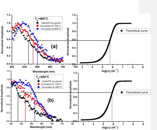
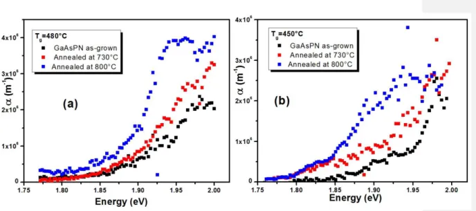
In the following, the composition of As is fixed at 10%, and sample set S2 was studied in some detail. The amplitude variations versus wavelength of the experimental normalized photothermal signal in the vicinity of the band gap energy are given in figure 4 (a) and (b) for the two samples of GaAsPN, which were grown at different temperatures under various annealing conditions. The amplitudes measured present two saturation levels for decreasing wavelengths below 640 nm and greater than 690 nm. The comparison between experimental curves and the corresponding theoretical ones [20, 23] permits us to assign for each wavelength the corresponding optical absorption coefficient resulting in the absorption spectra of the studied GaAsPN absorbers, as shown in figure 4. Figure 5 (a) and (b) show the absorption spectra of the two samples of GaAsPN for different growth temperatures and post-growth annealing conditions. From this figure, it is clear that the absorbance increases with increasing annealing temperature despite the shorter annealing time used at 800 °C (note that samples at 730°C annealing for 1 minute were also grown, showing nearly no difference in their optical properties compared to as-grown samples). This result is in contradiction with the one published in ref. [12], in which absorption coefficient is not improved with annealing. This may be attributed to the larger N content, typically around 2%, and the lower annealing temperature used in the present study. Indeed, in this study, we observe that annealing above 800°C damages the sample, preventing any improvement in photoluminescence properties. In fig. 3, it is also noticed that samples grown at 480°C and annealed at 800°C have a larger optical absorption (typically 40000 cm-1 at 1.95 eV) coefficient than those grown at 450 °C (typically 25000 cm-1 at 1.95 eV). This would tend to show that growth at 480°C favors the positioning of nitrogen atoms in crystalline sites, or anti-sites, which are more sensitive to post-growth annealing. Nevertheless, this still remains to be confirmed. Finally, the values obtained for optical absorption coefficients are in overall agreement with values extracted
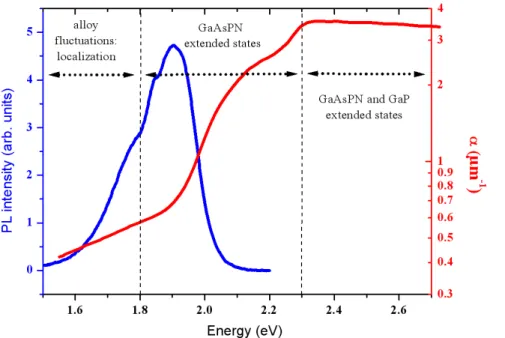
from direct optical absorption measurements of sample set 1: the small difference may be due to slightly different growth conditions, or light diffusion processes due to the roughness of the sample. This is also confirmed by direct optical absorption measurements performed on the sample grown at 480°C and annealed at 800°C (sample set 2), as illustrated in Fig. 6. In this figure, the corresponding photoluminescence spectrum is also shown. A detailed look at the PL spectrum in Fig. 6 shows it is composed of a low energy tail, usually associated with localized nitrogen states or alloy fluctuations [29], and a different peak at higher energy: around 1.9 eV. This higher energy-peak intensity was greatly improved during the annealing process, and corresponds well to the measured position of the absorption edge: with an associated Stockes shift below 100 meV in this system. This behavior, which is due to carrier localization, is very common in dilute nitride materials such as InGaAsN/GaAs,[30] and was already deeply studied by Karcher et al.[29] in the GaAsPN material system. Although it was beyond the scope of this paper we noted that a full analysis could be performed by studying the evolution of the maximum PL peak values with temperature, which displayed an unambiguous S-shaped behavior (not shown here). It is also clear from this figure that the interesting absorption range for tandem solar cell operation with such a GaAsPN absorber is between 1.8 eV and 2.3 eV: corresponding to the delocalized states of the GaAsPN bulk alloy. Annealing effects on optical absorption near the bandgap is not surprising because the incorporation of N in GaAsP results in the presence of randomly distributed nitrogen clusters and isolated nitrogen impurity states in the crystals [31, 32]. The application of post-growth annealing provides energy (related to the annealing temperature) for the change in group-V atom configuration i.e., a change in the nearest neighbor environment of Ga atoms. This globally leads to the reduction in defect density and an improvement in layer absorption. The effect of annealing on optical properties was also demonstrated in GaInAsN [33, 34], and the increase of GaAsPN/GaP quantum wells photoluminescence efficiency has already been reported [35].
From the experimental data presented here, the following interpretations can be given: (i) Annealing tends to limit the inhomogeneity of the samples (nitrogen localized states, alloy inhomogeneity, non-radiative centers), and favors the emission/absorption of the delocalized GaAsPN states (transition around 1.85 eV in this work). (ii) This effect is dependent on both temperature and annealing time. (iii) The sample grown at higher temperature (480°C) is more homogeneous before annealing than that grown at lower temperature (450°C).
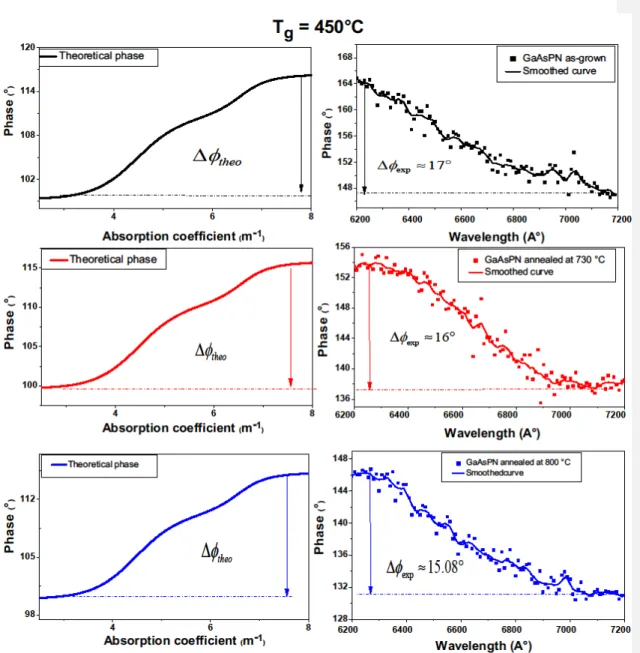
Thermal conductivity is a major parameter for improving quality and performance of solar cells [36, 37]. High thermal conductivity provides a number of advantages for optoelectronic and photonic devices by dissipating heat while the device is operating [38]. We evaluated the thermal conductivity of the two GaAsPN absorbers studied in sample set S2, which have shown themselves to be promising for use in tandem solar cells [11]. In the vicinity of the bandgap energy, the photothermal signal phase saturates in both high and low absorption regions. In the case of a thin semiconductor layer, the phase difference between the two saturations depends strongly on its thermal conductivity [20, 23]. We obtained the thermal conductivity of the two GaAsPN samples under different annealing conditions by varying the theoretical phase difference
∆
φ
theountil it is approximately equal to the experimental ones (∆
φ
theo≈ ∆
φ
exp). Figure 7 and 8 show the theoretical and the experimental phases of PDS signal for samples grown at 480°C and 450°C respectively. The extracted thermal conductivity values for samples from set S2 are listed in table 1.The first conclusion that can be drawn is that thermal conductivity increases with annealing temperature for the two samples presented here, reaching a value above 4 W/mK under the best annealing conditions (800°C) with a 480 °C growth temperature. Reduced overall thermal conductivity is usually associated with phonon scattering at boundaries and crystal point defects, both of which impose additional resistance [38, 39]. But it is also largely affected through the alloying process, [13] or superlattice interfaces [40], by the lattice order of the crystal. In the present study, the improvement of thermal conductivity with annealing is fully consistent with the analysis performed from absorption measurements, revealing better crystalline quality for materials grown at 480 °C and annealed at 800°C. Special attention should be paid to the inhomogeneity of the alloy: the presence of non-radiative centers or localized states are expected to play an important role here. Finally, it was shown in ref. [13] that the GaAs0.1P0.9 alloy has a thermal conductivity of 30 W/mK. Y. Zhao et al. measured the thermal conductivity of GaAsN with 2% of nitrogen to be around 27 W/mK, which is approximately 60% of the GaAs (thermal conductivity is 45 W/mK) binary system [14]. Taking into account the alloy disorder added by the quaternary alloy crystalline structure, as compared to ternary alloys, the values found in this work (around 4W/mK) are therefore consistent with what can be expected from reading the literature.
In this article, optical absorption and thermal conductivity of GaAsPN absorbers were investigated by means of optical absorption spectroscopy and photo-thermal deflection spectroscopy (PDS) for different GaAsPN/GaP samples with different growth conditions and various post-growth annealing temperatures. It was shown that optical absorption is strongly dependent on the As content in the alloy, and that absorbers with 10% of As and 2% of N are the most interesting as they guarantee, for tandem solar cell development on silicon, both the perfect lattice-matching and an absorption edge in the targeted [1.7-1.8 eV] range of energy. It was then shown that absorption spectra and thermal conductivity properties are significantly improved by the post-growth annealing process. This is attributed to the limitation of the structural inhomogeneity, which is larger when the sample has been grown at a lower temperature.
Acknowledgments:
The authors acknowledge J. Burdon for fruitful discussions. This research was supported by “Région Bretagne” through the PONANT project including FEDER funds. This work was also supported by the French national ANR projects MENHIRS (2011-PRGE-007-01) and SINPHONIC (2011 JS03 006-01).
References
[1] Xin Zhao, Dun Li , Brianna Conrad, Li Wang, Anastasia H. Soeriyadi, Martin Diaz, Anthony Lochtefeld, Andrew Gerger, Ivan Perez-Wurfl, Allen Barnett , Material and device analysis of SiGe solar cell in a GaAsP–SiGe dual junction solar cell on Si substrate, Solar Energy Materials and Solar Cells 134 (2015) 114-121
[2] K Akahori , G Wang , K Okumura, T Soga, T Jimbo, M Umeno, Improvement of the MOCVD-grown InGaP-on-Si towards high-efficiency solar cell application, Solar Energy Materials and Solar Cells 66 (2001) 593-598
[3] Yuji Komatsu, Keiji Hosotani, Takashi Fuyuki, Hiroyuki Matsunami, Heteroepitaxial growth of InGaP for extremely high-efficiency 2-terminal tandem solar cell with Si Solar Energy Materials and Solar Cells 35 (1994) 33-38.
[4] J. F. Geisz, D. J. Friedman, and S. Kurtz, GaNPAs solar cells lattice-matched to GaP, in: Conference Record of the Twenty-Ninth IEEE Photovoltaic Specialists Conference, 2002 pp. 864–867.
[5] J. F. Geisz, J. M. Olson, D. J. Friedman, K. M. Jones, R. C. Reedy, and M. J. Romero, Lattice-matched GaNPAs on silicon tandem solar cells,in: Conference Record of the Thirty-first IEEE Photovoltaic Specialists Conference, 2005,pp. 695–698.
[6] J. Geisz, J. M. Olson, W. E. McMahon, T. Hannappel, K. Jones, H. Moutinho, and M. M. Al-Jassim, Growth and Characterization of GaPNAs on Si, in: Progress in Compound Semiconductor Materials III - Electronic and Optoelectronic Applications, 2003, pp.27-31. [7] A. I. Baranov, A. S. Gudovskikh, E. V. Nikitina, and A. Y. Egorov, Photoelectric properties of solar cells based on GaPNAs/GaP heterostructures , Tech. Phys. Lett. 39 (2013) 1117–1120
[8] O. Durand , S. Almosni, C. Robert , T. T. Nguyen, Y. Wang , C. Cornet, A. Létoublon, C. Levallois , L. Pedesseau , J. Even , J.-M. Jancu , N. Bertru , A. Le Corre, A. Bondi , P. Râle, L. Lombez , J.-F. Guillemoles , E. Tea , S. Laribi, J. Stodolna , A. Ponchet , N. Boudet, Monolithic Integration of Diluted-Nitride III–V-N Compounds on Silicon Substrates,.in: Toward the III–V/Si Concentrated Photovoltaics. Energy Harvest Syst 2012, pp. 147–156
Code de champ modifié Code de champ modifié Code de champ modifié Code de champ modifié Code de champ modifié Code de champ modifié Code de champ modifié Code de champ modifié Code de champ modifié Code de champ modifié Code de champ modifié Code de champ modifié Code de champ modifié Code de champ modifié Code de champ modifié Code de champ modifié Code de champ modifié Code de champ modifié Code de champ modifié Code de champ modifié Code de champ modifié Code de champ modifié Code de champ modifié Code de champ modifié
Code de champ modifié Code de champ modifié Code de champ modifié Code de champ modifié Code de champ modifié Code de champ modifié Code de champ modifié
[9] H. P. Xin, C. W. Tu, Y. Zhang, and A. Mascarenhas, Effects of nitrogen on the band structure of GaNxP1− x alloys, Appl. Phys. Lett. 76 (2000) 1267–1269.
[10] I. A. Buyanova, G. Pozina, J. P. Bergman, W. M. Chen, H. P. Xin, and C. W. Tu, Time-resolved studies of photoluminescence in GaNxP1− x alloys: Evidence for indirect-direct band gap crossover, Appl. Phys. Lett., 81 ( 2002) 52–54.
[11] S. Almosni, C. Robert, T. Nguyen Thanh, C. Cornet, A. Letoublon, T. Quinci, C. Levallois, M. Perrin, J. Kuyyalil, L. Pedesseau, A. Balocchi, P. Barate, J. Even, J. M. Jancu, N. Bertru, X. Marie, O. Durand, and A. Le Corre, Evaluation of InGaPN and GaAsPN materials lattice-matched to Si for multi-junction solar cells, J. Appl. Phys 113 (2013) 123509 [12] R. Kudrawiec,A.V. Luce, M. Gladysiewicz, M. Ting, Y.J. Kuang, C.W. Tu, C.W. Tu, O.D. Dubon, K.M. Yu and W. Walukiewicz, Electronic Band Structure of GaNxPyAs1−x−y Highly Mismatched Alloys: Suitability for Intermediate-Band Solar Cells, Phys. Rev. Appl. 1 (2014) 034007
[13] S. Adachi, Lattice thermal conductivity of group-IV and III–V semiconductor alloys, J. Appl. Phys. 102 (2007) 063502
[14]Y.M. Zhao, G. Chen, S.Z. Wang, S.F. Yoon , Thermal characterization of gallium arsenic nitride epilayer on gallium arsenide substrate using pulsed photothermal reflectance technique, Thin Solid Films, 450 (2004) 352-356
[15] A. Utsumi, H. Yonezu, Y. Furukawa, K. Momose, and K. Kuroki, Increase in luminescence efficiency of GaPN layers by thermal annealing, Phys. Status Solidi C. 0 (2003) 2741–2744.
[16] M. Izadifard, I. A. Buyanova, J. P. Bergman, W. M. Chen, A. Utsumi, Y. Furukawa, A. Wakahara, and H. Yonezu, Effects of rapid thermal annealing on optical quality of GaNP alloys, Optoelectron. IEE Proc. 151 (2004),pp 335–337
[17] A. C. Boccara, D. Fournier, and J. Badoz, Thermo-optical spectroscopy: Detection by the”mirage effect”, Appl. Phys. Lett. 36 (1980) 130
[18] N. M. Amer and W. B. Jackson, Optical Properties of Defect States in a-Si:H in Hydrogenated Amorphous Silicon, J. I. Pankove, ed., Semiconductors and Semimetals Academic Press, Orlando,21 (1984)
[19] A. Rosencwaig and A. Gersho, Theory of the photoacoustic effect with solids, J. Appl. Phys. 47 (1976) 64
[20] N. Yacoubi and C. Alibert, Determination of very thin semiconductor layer thickness by a photothermal method, J. Appl. Phys. 69 (1991) 12
Code de champ modifié
Code de champ modifié
Code de champ modifié
Code de champ modifié
Code de champ modifié
Code de champ modifié
Code de champ modifié
[21] J. C. Murphy and L. D. Aamodt, Photothermal spectroscopy using optical beam probing: mirage effect, J. Appl. Phys. 51 (1980) 4580
[22] N. Yacoubi, A. Hafaiedh and A. Joullié, Determination of the optical and thermal properties of semiconductors with the photothermal method, Applied Optics 33 (1994) 7171-7174
[23] S. Ilahi ,F. Saidi, R. Hamila , N. Yacoubi , L. Auvray , H. Maaref, Photothermal deflection spectroscopy PDS investigation of optical and thermal properties of BGaAs/GaAs alloys, Current Applied Physics 13 (2013) 610-613.
[24] T. Quinci, J. Kuyyalil, T.Nguyen Thanh, Y.Ping Wang, S. Almosni, A. Létoublon, T. Rohel, K. Tavernier, N. Chevalier, O. Dehaese, N. Boudet, J.F. Bérar, S. Loualiche, J. Even, N. Bertru, A. Le Corre, O. Durand, C. Cornet, Defects limitation in epitaxial GaP on bistepped Si surface using UHVCVD–MBE growth cluster, J. Cryst. Growth. 380 (2013) 157. [25] J. Kuyyalil, T. Nguyen Thanh, T. Quinci, S.Almosni, A. Létoublon, T. Rohel, N. Bertru, A. Le Corre, O. Durand, C. Cornet, Nitrogen–phosphorus competition in the molecular beam epitaxy of GaPN, J. Cryst. Growth. 377 (2013) 17.
[26] C. Cornet, T. T. Nguyen, T. Quinci, S. Almosni, T. Rohel, J. Kuyyalil, A. Rambaud, A. Létoublon, N. Bertru, O. Durand, A. Le Corre, Preferential incorporation of substitutional nitrogen near the atomic step edges in diluted nitride alloys, Applied Physics Letters, 101 (2012) 251906.
[27] C. Robert, M. Perrin, C. Cornet, J. Even, J.-M. Jancu, Atomistic calculations of Ga(NAsP)/GaP(N) quantum wells on silicon substrate: Band structure and optical gain Applied Physics Letters, 100 (2012) 111901.
[28] C. Robert, A. Bondi, T. T. Nguyen, J. Even, C. Cornet, O. Durand, J.-P. Burin, J.-M. Jancu, W. Guo, A. Létoublon, H. Folliot, S. Richard, M. Perrin, N. Chevalier, O. Dehaese, K. Tavernier, S. Loualiche, A. Le Corre, Room temperature operation of GaAsP(N)/GaP(N) quantum well based light-emitting diodes: Effect of the incorporation of nitrogen, Applied Physics Letters, 98 (2011) 251110
[29] C. Karcher, K. Jandieri, B. Kunert, R. Fritz, M. Zimprich, K. Volz, W. Stolz, F. Gebhard, S. D. Baranovskii, and W. Heimbrodt, Peculiarities of the photoluminescence of metastable Ga (N, As, P)/GaP quantum well structures, Phys. Rev. B 82 (2010) 245309
[30] L. Grenouillet, C. Bru-Chevallier, and G. Guillot P. Gilet, P. Duvaut, C. Vannuffel, A. Million, and A. Chenevas-Paule, Evidence of strong carrier localization below 100 K in a GaInNAs/GaAs single quantum well, App Phys Lett 76 (2000) 2241
Code de champ modifié
Code de champ modifié
Code de champ modifié
Code de champ modifié
Code de champ modifié
Code de champ modifié
Code de champ modifié
[31] H. Saito, T. Makimoto, T. Nishida, N. Kobayashi, Excitonic luminescence and absorption in dilute GaAs 1-x N x alloy (x≪ 0.3%), Appl. Phys. Lett. 70 (1997) 2984 [32] S. Francoeur, S.A. Nikishin, C. Jin, Y. Qiu, H. Temkin, Excitons bound to nitrogen clusters in GaAsN, Appl. Phys. Lett. 75 (1999) 1538
[33] K. Volz, J. Koch, B. Kunert, I. Nemeth, and W. Stolz, Influence of annealing on the optical and structural properties of dilute N-containing III/V semiconductor heterostructures, J. Cryst. Growth 298 (2007) 126-130
[34] O. Rubel, M. Galluppi, S. D. Baranovskii, K. Volz, L. Geelhaar, H. Riechert, P. Thomas, and W. Stolz, Quantitative description of disorder parameters in (GaIn)(NAs) quantum wells from the temperature-dependent photoluminescence spectroscopy, J. Appl. Phys. 98 (2005) 063518.
[35] B. Kunert, D. Trusheim, V. Voßebürger, K. Volz, and W. Stolz , Annealing experiments of the GaP based dilute nitride Ga (NAsP), Phys. stat. sol. (a) 205 (2008) 114– 119
[36] F.M. Gaitho, F.G. Ndiritu, P.M. Muriithi, R.G. Ngumbu, J.K. Ngareh. Effect of thermal conductivity on the efficiency of single crystal silicon solar cell coated with an anti-reflective thin film, Solar Energy. 83 (2009) 1290–1293
[37] E. Radziemska, Thermal performance of Si and GaAs based solar cells and modules: a review, Progress in Energy and Combustion Science. 29 (2003) 407–424
[38] Terry M. Tritt. Book “Thermal Conductivity: Theory, Properties, and Applications” (2004), pp.168-169,
[39] D. Bimberg, F.Heinrichsdorff, R.K.Bauer, D Gerthsen, D.Stenkamp,D.E.Mars and J.N. Miller , Binary AlAs/GaAs versus ternary GaAlAs/GaAs interfaces: a dramatic difference of perfection, J. Vac. Sci. Techno B. 10 (1992) 1793
[40] X. Y. Yu, G. Chen, A. Verma and J. S. Smith, Temperature dependence of thermophysical properties of GaAs/AlAs periodic structure, Appl. Phys. Lett. 67 (1995) 3554
Code de champ modifié
Code de champ modifié
Code de champ modifié
Code de champ modifié
Code de champ modifié
Code de champ modifié Code de champ modifié Code de champ modifié Code de champ modifié Code de champ modifié Code de champ modifié Code de champ modifié Code de champ modifié Code de champ modifié Code de champ modifié
Code de champ modifié
Tables K (W/mK) As-grown K (W/mK) GaAsPN (730°C) K (W/mK) of GaAsPN (800°C) Tg=480°C 2.40 (1.25%) 3.80 (0.9%) 4.30 (0.86%) Tg=450°C 1.75 (1.1%) 2.10 (1%) 2.30 (1.3%)
Table 1. Thermal conductivities of GaAsPN grown at 450°C and 480°C as a function of annealing conditions.
Figure captions
Table 1. Thermal conductivities of GaAsPN grown at 450°C and 480°C as a function of
annealing conditions.
Figure 1.Outline of the different media used in the model
Figure 2. Sketch of the experimental PTD setup.
Figure 3. Optical absorption coefficient measured for various As content values (5%, 10%,
30% and 40%) in 100nm-thick GaAsPN absorbers (set of samples S1).
Figure 4. Determination of absorption spectrum by comparison between the experimental and
theoretical amplitude for the GaAsPN layers grown at 480°C (a) and 450°C (b) (set of
samples S2).
Figure 5. Absorption spectra of GaAsPN layers grown at 480°C ((a) and 450°C (b) (set of
samples S2).
Figure 6. Room temperature photoluminescence spectra of GaAsPN grown at Tg=480°C (set
of samples S2) annealed at 800 °C, with the corresponding absorption spectrum
Figure 7. Comparison between experimental and theoretical phase difference near the gap
layer of GaAsPN grown at 480 °C (set of samples S2).
Figure 8. Comparison between experimental and theoretical phase difference near the gap
Figure 1.Outline of the different media used in the model
Figure 3. Optical absorption coefficient measured for various As content values (5%, 10%, 30% and 40%) in 100nm-thick GaAsPN absorbers (set of samples S1).
Figure 4. Determination of absorption spectrum by comparison between the experimental and theoretical amplitude for the GaAsPN layers grown at 480°C (a) and 450°C (b) (set of
Figure 5. Absorption spectra of GaAsPN layers grown at 480°C ((a) and 450°C (b) (set of samples S2).
Figure 6. Room temperature photoluminescence spectra of GaAsPN grown at Tg=480°C (set of samples S2) annealed at 800 °C, with the corresponding absorption spectrum.
Figure 7. Comparison between experimental and theoretical phase difference near the gap layer of GaAsPN grown at 480 °C (set of samples S2).
Figure 8. Comparison between experimental and theoretical phase difference near the gap layer of GaAsPN grown at 450 °C (set of samples S2).