3
ACKNOWLEDGEMENTS
It is my pleasure to express my deep sense of thanks to several individuals who were instrumental in completion of my PhD.
First and foremost, I would like to express my sincere gratitude to my mentors and supervisors Dr. Erik Dujardin and Dr. Aurélien Cuche for all their valuable suggestions, guidance and unconditional support over the period of my PhD through both good times and bad times. I truly enjoyed working in an environment which stimulates original thinking and initiative which they created. Their guidance, innovative ideas and stoic patience are greatly appreciated. I would like to acknowledge the valuable inputs from Dr. Christian Girard who was always happy to discuss, assist and resolve most difficult modelling issues. His timely advices have immensely helped in shaping my research. I would also like to pass on my sincere vote of thanks to Dr. Alexandre Bouhelier for hosting me several times at Dijon and providing me chance to work on his state of art of lab at ICB, Dijon. Special thanks to Dr. Sviatlana Viarbitskaya for her help during the experimental missions at Dijon.
These acknowledgements would not be complete without mentioning my lab and office colleagues: Bulent Baris, Janak Prasad, Marie Herve, Mohanad Alchar, Laureen Moreaud, Marc Nunez, Victor Freire, Delphine Sordes and Benoit Eydoux. It was great working with them and I really appreciate their ideas, help and good humour.
Aside from the main physics crowd, I would also like to thank those who were and still are there for me outside my lab. Thanks to Prerna Bagri, Raghuveer Kasaraneni, Vandita Banka, Hari Prasath, Aishwarya Balaji, Alok Singh, Neeti Singh and Anvika Singh for making my stay at Toulouse pleasant and a memorable one.
Lastly and most importantly, I would like to thank my parents and other family members who are eagerly waiting for my return, for their patience, continuous support and encouragement. It is of no surprise that I dedicate this work to them. With regards to the numerous questions about my future endeavours from family and friends, I shall answer in the words of Sir Winston Churchill: “Now this is not the end, it is not even the beginning of the end. But, it is perhaps the end of the beginning”.
5
Table of Contents
I Motivations ... 9
II Introduction ... 15
2.1 Introduction to plasmonics ... 15
2.1.1 Surface plasmon polaritons ... 16
2.1.2 Localized Surface Plasmons ... 21
2.1.3 Micrometre sized metallic structures ... 23
2.2 Local density of states ... 24
2.2.1 Photonics LDOS ... 25
2.2.2 Surface plasmon local density of states (SPLDOS) ... 27
2.2.3 Non-linear photon luminescence and SPLDOS ... 28
2.3 Single crystalline colloidal system... 30
2.3.1 Top down and bottom up approaches ... 30
2.3.2 Crystalline colloidal systems for reconfigurable plasmonic devices ... 32
III Materials and methods... 39
3.1 Experimental fabrication and characterization techniques ... 39
3.1.1 Wet Chemical synthesis ... 39
3.1.2 Focussed Ion Beam ... 40
3.1.3 Dark field scattering microscopy ... 42
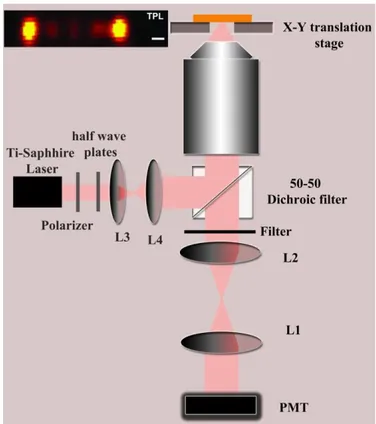
3.1.4 Non-linear photon luminescence microscopy ... 45
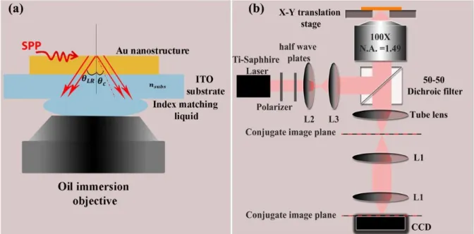
3.1.5 Leakage radiation microscopy ... 48
3.2 Simulation techniques ... 50
3.2.1 Green Dyadic Method ... 50
3.2.2 Transmission Maps ... 53
3.2.3 SPLDOS and TPL Maps ... 56
IV Spectral engineering of two – dimensional plasmonic nanoprisms ... 63
4.1 Introduction ... 63
6
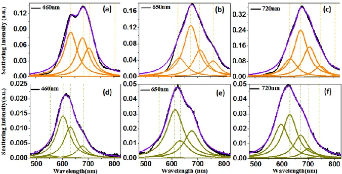
4.2.1 Spectral response of Au nanoprisms and Lorentzian decomposition ... 64
4.2.2 Variation of spectral features with size of the cavity ... 67
4.3 Spectral control of SP resonances in a MIM configuration ... 71
4.3.1 Spectral response of Au nanoprisms on 30nm thin Au film ... 71
4.3.2 Tuning of spectral responses of Au prism with different metallic substrates ... 75
4.4 Spectral response of Au nanoprism in presence of hole ... 76
4.5 Conclusions ... 79
V Multimodal bowtie antennas for efficient far-field to near-field conversion ... 84
5.1 Introduction ... 84
5.2 TPL response of the multimodal bowtie antenna ... 85
5.3 Local field enhancement and multiscale nature of the antennas ... 91
5.4 Conclusions ... 94
VI Designing transmission eigenstates for tailoring SPP propagation in 2D plasmonic device... 99
6.1 Introduction ... 99
6.2 Computation of the transmission maps ... 101
6.2.1 Excitation of the diabolo structure by a dipole ... 101
6.2.2 Excitation of the diabolo structure by a Gaussian shaped plane wave ... 102
6.2.3 Excitation of the diabolo structure by real Gaussian function ... 103
6.3 Designing of diabolo ... 104
6.4 Transmittance of plasmonic signal in a 2D diabolo cavity ... 106
6.4.1 Tuning of transmittance with incident polarization and excitation position... 108
6.4.2 Tuning of transmittance with incident wavelength ... 117
6.4.3 Spectral detuning in asymmetrical diabolo ... 117
6.5 Conclusion ... 120
VII Reconfigurable modal plasmonic logic gates ... 124
7.1 Introduction ... 124
7.2 Gedanken Experiment ... 126
7
7.4 Realization of modal logic gates on double hexagon structures ... 133
7.4.1 Numerical proof of the principle... 133
7.4.2 Experimental implementation ... 135
7.5 Reconfiguration of the modal plasmonic logic gates ... 138
7.5.1 Reconfiguration of logic gates with different threshold ... 138
7.5.2 Reconfiguration based on different set of input locations ... 140
7.5.3 Reconfiguration based on different set of polarizations ... 141
7.6 Conclusion ... 143
VIII Conclusions and future perspectives ... 147
Résumé en français de la thèse ... 153
9
Chapter I
Motivations
In 1959, when Richard Feynman said “There is plenty of room at the bottom” [1], his statement was not received so enthusiastically by the scientific community. But in a little more than a decade, the interest for the nano-world had increased rapidly leading to the emergence of a new field called nanotechnology [2]. Besides electronics, one of the fields of nanotechnology that has undergone a remarkable expansion and progress is plasmonics, the technology based on the interaction between free electrons in noble metals and impinging electromagnetic fields [3], [4]. The plasmon resonances can be categorized in two types – surface plasmon polaritons (SPP), which are collective electronic waves propagating along a metal-dielectric interface and localized surface plasmon, (LSP) which are confined oscillations of surface electrons on a metal nanoparticle. Research on plasmons has essentially investigated the properties of either macroscopic metallic structures that facilitate propagation, wave guiding and routing of SPP or nanometre-scale metallic particles that produce intense resonances and a strong field confinement.Beyond a wealth of fascinating physics, this field has generated innovative applications ranging from superfast computer [5], [6] to treatment of cancer [7], [8] , highly sensitive molecular detectors [9], data storage devices [10], [11], optical information processing [12], [13] , quantum optics [14], [15] etc.
Surprisingly, much less attention has been paid to an intermediate regime of micrometer-sized structures in which both localized LSP resonances and propagating SPP co-exist and contribute equivalently to the optical properties of the structure. This doctoral work is dedicated to a comprehensive study of individual metallic structures in this intermediate size regime and will explores new possible applications in plasmon-based information processing.
So far, the most advanced plasmonic devices and interconnects are produced by a standard top-down microfabrication approach [16]. In the micrometer-size range, the performances of such devices are limited are by scattering-related energy dissipation which essentially originates in the amorphous or polycrystalline nature of the original metallic film
[17]. More than a decade ago, it was shown that chemically produced crystalline nanowire suffered comparatively less energy dissipation than top-down fabricated plasmonic waveguide
10
of identical geometry [18]. This was generalized to flat two-dimensional plasmonic antennas carved out inside thin crystalline gold plates [19]. Information processing circuits and prototypes exploiting the properties of crystalline nanowires of flakes have been demonstrated. However, generally, the working principle involves the encoding of both the input information and the transfer function of the device in the form of polarization or wavelength of the incident beam(s). For example, a full family of logic gates was recently realized using polarization and phase dependent interferences between plasmon signals propagating along silver nanowires
[20]. While complex logic gate functions have been reported by cascading elementary logic gates [20], [21], the performances of such interferential devices are limited by the precision of the relative positioning of the active building blocks with respect to each other and of the excitation spot.
In this thesis, we propose to revert this paradigm, i.e. to design plasmonic devices in two dimensions and in a size regime that confers them with characteristic confined resonances or modes independently from the excitation configuration. We will seek to tailor and control the spectral and spatial behaviour of the mesoscale structures, to exploit them for capturing photons to excite plasmons, routing plasmonic signal from one point to another and to explore new ideas for the realization of complex plasmonic modal logic gates.
Chapter II of this thesis provides a brief introduction to the field of plasmonics. Plasmon phenomena are exposed along with the basic models describing them. Next we detail the concept of local density of plasmonic states which conveniently describes the properties of objects bearing a large but finite number of modes. The chapter concludes by a description of the specific crystalline plasmonic nanoparticles used in this work. These are ultrathin triangular or hexagonal platelets with lateral dimensions comprised between 0.5 and 5.0 m.
The third chapter collects the technical details regarding all the experimental fabrication procedures and characterization techniques used throughout the thesis. A detailed section is dedicated to the description of simulation tools based on Green Dyadic Method developed by Christian Girard (CEMES). All the simulations presented in this work were performed using these codes.
In chapter IV, we present, a systematic study of the spectral properties of sharp triangular gold nanoprisms as their size is increased from 400nm to 900nm. These objects host a collection of resonances the characteristics of which will be experimentally examined and compared to simulations. Next we wondered if the spectral response of the gold nanoprisms
11
supported on glass could be altered by the presence of a nearby thin metal film or by the introduction of a hollow defect in the gold nanoprism.
Chapter V will focus on one first information processing function: far-field to near-field conversion antennas. A bowtie antenna configuration will be constructed by the coupling between two of these crystalline mesoscale prisms. The effect of the relative size of the prism cavities will be studied. In particular, we will investigate, whether, the incident polarization and relative position of one cavity with the other have an effect on the properties of the antenna. In chapter VI, we will focus on the ways to transmit information from one incident point to another emitting point by exciting delocalized modes with well-defined spatial distribution. For this we will consider introducing a rectangular channel connecting two individual triangular cavities in a diabolo-like geometry. A comprehensive experimental and numerical study of the plasmon transmittance will be conducted by examining the effects of changing the incident polarization, the excitation position, the relative size of the two prisms or the excitation wavelength. This study will indicate how a tailored two dimensional metallic cavity can be relevant to the design of more complex modal plasmonics devices
Chapter VII presents the most advanced proposal of this work as it described the design and implementation of a modal plasmonic architecture realizing the function of Boolean logic gates. Gedanken experiments proposed earlier in our group will be experimentally implemented for the first time. In particular, we will demonstrate how to create 2-input, 1-output logic gates based on the modal features of the 2D metallic structures. In the final part of this chapter, we will investigate the concept of reconfigurable logic gates that demonstrates the high potential of our non-conventional approach for creating even more complex information processing devices.
12
References
[1] R. P. Feynman, “There’s plenty of room at the bottom: An invitation to enter a new field of physics,” Eng. Sci., vol. 23, pp. 22–35, 1960.
[2] E. K. Drexler, “Molecular Machinery and Manufacturing With Applications to Computation,” Engineering, no. 1977, pp. 1–487, 1977.
[3] L. Novotny and B. Hecht, "Principles of Nano-Optics", Cambridge University Press, 2nd Ed., no. 1. 2012.
[4] S. A. Maier, “Plasmonics: Fundamentals and Applications,” Springer, 2007.
[5] H. A. Atwater, “The promise of plasmonics,” ACM SIGDA Newsl., vol. 37, no. 9, pp. 1–1, 2007. [6] J. R. Kerrn, “Perspective on plasmonics,” Nat. Photonics, vol. 6, no. 11, pp. 714–715, 2012.
[7] C. Yang, L. Ma, X. Zou, G. Xiang, and W. Chen, “Surface plasmon-enhanced Ag/CuS nanocomposites for cancer treatment,” Cancer Nanotechnol., vol. 4, no. 4–5, pp. 81–89, 2013.
[8] S. B. Lakshmanan, X. Zou, M. Hossu, L. Ma, C. Yang, and W. Chen, “Local field enhanced Au/CuS nanocomposites as efficient photothermal transducer agents for cancer treatment,” J. Biomed. Nanotechnol., vol. 8, no. 6, pp. 883–890, 2012.
[9] J. N. Anker, W. P. Hall, O. Lyandres, N. C. Shah, J. Zhao, and R. P. Van Duyne, “Biosensing with plasmonic nanosensors,” Nat. Mater., vol. 7, no. 6, pp. 442–453, 2008.
[10] D. O’Connor and A. V. Zayats, “Data storage: The third plasmonic revolution,” Nat. Nanotechnol., vol. 5, no. 7, pp. 482–483, 2010.
[11] P. Zijlstra, J. W. M. Chon, and M. Gu, “Five-dimensional optical recording mediated by surface plasmons in gold nanorods,” Nature, vol. 459, no. 7245, pp. 410–413, 2009.
[12] B. Lamprecht, J. R. Krenn, G. Schider, H. Ditlbacher, M. Salerno, N. Felidj, A. Leitner, and F. R. Aussenegg, “Surface plasmon propagation in microscale metal stripes,” Appl. Phys. Lett., vol. 79, no. 1, pp. 51–53, 2001.
[13] J. Liu, G. Fang, H. Zhao, Y. Zhang, and S. Liu, “Plasmon flow control at gap waveguide junctions using square ring resonators,” J. Phys. D. Appl. Phys., vol. 43, no. 5, p. 55103, 2010.
[14] D. E. Chang, A. S. Sorensen, P. R. Hemmer, and M. D. Lukin, “Quantum optics with surface plasmons,” Phys. Rev. Lett., vol. 97, no. 5, 2006.
[15] A. V. Akimov, A. Mukherjee, C. L. Yu, D. E. Chang, A. S. Zibrov, P. R. Hemmer, H. Park and M. D. Lukin, “Generation of single optical plasmons in metallic nanowires coupled to quantum dots,” Nature, vol. 450, no. 7168, pp. 402–406, 2007.
[16] W. Pfaff, A. Vos, and R. Hanson, “Top-down fabrication of plasmonic nanostructures for deterministic coupling to single quantum emitters,” J. Appl. Phys., vol. 113, no. 2, 2013.
[17] A. Trügler, J.-C. Tinguely, J. R. Krenn, A. Hohenau, and U. Hohenester, “Influence of surface roughness on the optical properties of plasmonic nanoparticles,” Phys. Rev. B, vol. 83, no. 8, p. 81412, 2011. [18] H. Ditlbacher, A. Hohenau, D. Wagner, U. Kreibig, M. Rogers, F. Hofer, F. R. Aussenegg, and J. R.
Krenn, “Silver Nanowires as Surface Plasmon Resonators,” Phys. Rev. Lett., vol. 95, no. 25, p. 257403, 2005.
[19] J.-S. Huang, V. Callegari, P. Geisler, C. Brüning, J. Kern, J. C. Prangsma, X. Wu, T. Feichtner, J. Ziegler, P. Weinmann, M. Kamp, A. Forchel, P. Biagioni, U. Sennhauser and B. Hecht “Atomically flat
single-13
crystalline gold nanostructures for plasmonic nanocircuitry,” Nat. Commun., vol. 1, no. 9, p. 150, 2010. [20] H. Wei, Z. Wang, X. Tian, M. Käll, and H. Xu, “Cascaded logic gates in nanophotonic plasmon networks,”
Nat. Commun., vol. 2, p. 387, 2011.
[21] H. Wei and H. Xu, “Nanowire-based plasmonic waveguides and devices for integrated nanophotonic circuits,” Nanophotonics, vol. 1, no. 2, pp. 155–169, 2012.
15
Chapter II
Introduction
2.1 Introduction to Plasmonics
The invention of laser in 1960 brought a revolution in the field of optics and photonics which has since then grown into an important technology with widespread applications including optical information processing. The development in silicon photonics have resulted in the realization of small on-chip devices which enable routing and modulation of optical signals [1]. Few examples of photonics based devices which have been demonstrated on small chips are optical switches, optical modulators, optical sensors, photonic interconnects, photonic waveguides, etc. [2]–[5]. These photonic devices, however, are diffraction limited which means that, it is not possible to confine light into the regions that are smaller than its wavelength
[6]. This diffraction limit can be overcome by using photons to excite surface plasmons, which provide us a way to manipulate and guide light at a sub-wavelength scale via strong electromagnetic field confinement [7], [8].
The scientific investigation of plasmonic effects began as early as 1902 by Robert Wood when he observed a dark band in spectrum of light diffracted from a metallic grating which is now called Wood’s anomalies [9]. It was followed by the physical interpretation of the phenomenon by Lord Rayleigh [10] in 1907 who suggested that the anomaly in the spectrum of diffracted light takes place at a wavelength for which the scattered wave emerges tangentially to the surface. It took a couple of decades before Ugo Fano predicted the existence of polarized quasi stationary waves resonating along metal surface associated with these anomalies [11]. In 1957, R. H. Ritchie recorded loss of energy of an electron beam when diffracted at thin metallic foils [12]. He predicted that this energy loss is due to the coherent excitations of electrons inside the metal which were later on termed as surface plasmons. However, it was not before 1968 that the systematic study of the surface plasmon could start, when Erich Kretschmann [13] and Andreas Otto [14], almost simultaneously came up with techniques to optically excite surface plasmons. In last five decades, with the breakthroughs in various nanofabrication and characterization techniques and development of electromagnetic modelling, plasmonics has evolved from a physical phenomenon to an optical technology which has kept researchers across the spectrum interested.
16
2.1.1 Surface plasmon polaritons
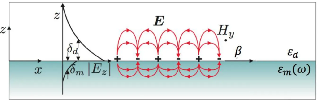
Surface plasmon polaritons (SPP) are two dimensional electromagnetic wave travelling along an interface between materials with dielectric constants of opposite sign (i.e. a conductor and a dielectric) and evanescent in the direction perpendicular to the interface. The schematic of a SPP propagating along a metal-dielectric interface is shown in figure 2.1.
Figure 2.1 Schematic of SPP propagation at an interface of metal and dielectric with dielctric constants εm(ω) and εd respectively.
The SPP waves are propagating along the x axes and the field has no spatial dependence along the y-direction. The x-y plane overlaps with the interface between a metal with a dielectric constant εm(ω) and a dielectric medium (z > 0) with the positive dielectric constant εd. These evanescent waves confined to the interface exists only for transverse magnetic (TM) polarization where field components Ex, Ez and Hy are non zero. For TE modes, field
components Hx, Hz and Ey are non zero and are given by –
𝐸𝑦(𝑧) = 𝐴2 𝑒𝑖𝛽𝑥𝑒−𝑘𝑑𝑧 (2.1a) 𝐻𝑥(𝑧) = −𝑖𝐴2 1 𝜔𝜇0𝑘2 𝑒 𝑖𝛽𝑥𝑒−𝑘𝑑𝑧 (2.1b) 𝐻𝑧(𝑧) = −𝑖𝐴1 1 𝜔𝜇0 𝑒 𝑖𝛽𝑥𝑒−𝑘𝑑𝑧 (2.1c) for z > 0 and 𝐸𝑦(𝑧) = 𝐴1 𝑒𝑖𝛽𝑥𝑒−𝑘𝑚𝑧 (2.1d) 𝐻𝑥(𝑧) = −𝑖𝐴1 1 𝜔𝜇0 𝑘1𝑒 𝑖𝛽𝑥𝑒−𝑘𝑚𝑧 (2.1e) 𝐻𝑧(𝑧) = −𝑖𝐴1 1 𝜔𝜇0 𝑒 𝑖𝛽𝑥𝑒−𝑘𝑚𝑧 (2.1f)
17
for z < 0. Here, Hx and Ey will be continuous at the interface only when
𝐴1(𝑘𝑑+ 𝑘𝑚) = 0 (2.2) Since kd and km are both of same sign, the condition can be fulfilled only when A1 and A2 both
are zero.
Thus, SPP modes is only possible with the TM polarization where the electric field, E is parallel to the plane of incidence and thus we have component of electric field along x and z directions. To better understand this, let us first consider the solutions of the propagating wave confined to the interface for TM polarization [15] –
𝐻𝑦(𝑧) = 𝐴2 𝑒𝑖𝛽𝑥𝑒−𝑘𝑑𝑧 (2.3a) 𝐸𝑥(𝑧) = −𝑖𝐴2 1 𝜔𝜀0𝜀2𝑘2 𝑒 𝑖𝛽𝑥𝑒−𝑘𝑑𝑧 (2.3b) 𝐸𝑧(𝑧) = −𝑖𝐴1 1 𝜔𝜀0𝜀2 𝑒 𝑖𝛽𝑥𝑒−𝑘𝑑𝑧 (2.3c) for z > 0 and 𝐻𝑦(𝑧) = 𝐴1 𝑒𝑖𝛽𝑥𝑒−𝑘𝑚𝑧 (2.3d) 𝐸𝑥(𝑧) = −𝑖𝐴1 1 𝜔𝜀0𝜀1 𝑘1𝑒 𝑖𝛽𝑥𝑒−𝑘𝑚𝑧 (2.3e) 𝐸𝑧(𝑧) = −𝑖𝐴1 1 𝜔𝜀0𝜀1 𝑒 𝑖𝛽𝑥𝑒−𝑘𝑚𝑧 (2.3f)
for z < 0. For continuity of Ex, Ez and Hy at the interface, A1 and A2 must be equal we must
fulfil following conditions -
𝑘𝑑 𝑘𝑚= − 𝜀𝑑 𝜀𝑚 (2.4a) 𝑘𝑚2 = 𝛽2− 𝑘02𝜀𝑚 (2.4b) 𝑘𝑑2 = 𝛽2− 𝑘02𝜀𝑑 (2.4c) Combining above three relations results in the dispersion relation for SPP propagating along the interface which is given by -
18 𝛽 = 𝑘0√
𝜀𝑚(𝜔)𝜀𝑑
𝜀𝑚(𝜔)+𝜀𝑑 (2.5)
where 𝛽 is the SPP propagation constant. The SPPs exponentially decay in the dielectric and the metallic mediums as shown in the figure 2.1. The penetration depths 𝛿𝑑 and 𝛿𝑚 respectively in the two mediums are given by –
𝛿𝑖 = 𝜆 2𝜋√
𝑅𝑒|𝜀𝑚|+𝜀𝑑
(𝜀𝑖)2 (2.6)
where ‘i’ denotes the medium in which SPP is penetrating. The corresponding SPP dispersion curve is shown in figure 2.2 along with the dispersion curve for a free space photon. The figure shows that the SPP dispersion relation curve is always placed to the right of the light line. A momentum projection of photons falling on the interface at an angle ‘’ to the normal surface, 𝑘𝑥 = 𝑘0𝑠𝑖𝑛𝜃 will always be smaller than 𝛽. This condition makes it impossible to excite the SPP with a standard propagating electromagnetic wave. Before discussing the possible techniques to excite SPP, it is worth understanding damping and losses mechanism in SPPs. The dielectric constant of metal, 𝜀𝑚(𝜔) in the dispersion relation consists of both real and imaginary components. The imaginary part of the dielectric constant describes the energy dissipation due to electron oscillations in the metal which is also called as Ohmic damping. This imaginary part of the dielectric constant also appears in the solution for the SPPs in form of an exponentially decaying damping term which leads to an SPP propagation length given by
𝛿𝑆𝑃 = 1
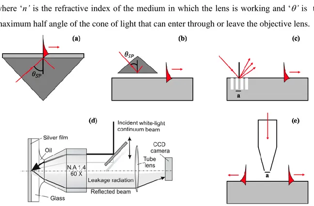
2𝐼𝑚(𝛽) (2.7) The momentum of light and SPP can be matched using different coupling configurations based on uses of prisms [13], [14], grating [16]–[18], optical fibre tip [19], and high numerical aperture objective lens [20]. There are basically two different prism based SPP excitation techniques. Both techniques are based on the coupling of the SPPs to the evanescent electromagnetic field that is formed upon total internal reflection of a light beam at the surface of a thin metal film. The first configuration is called the Kretschmann configuration [13] where, the metal film is evaporated on top of a glass prism and is then illuminated through the dielectric prism at an angle of incidence greater than the critical angle. Now, the light reflected at the interface between the prism and the metal film has an in-plane momentum of 𝑘𝑥= 𝑘0√𝜖𝑝𝑟𝑖𝑠𝑚 𝑠𝑖𝑛𝜃. Under these conditions, the resonant light tunnel through the thin metal layer and couples to the SPP.
19
Figure 2.2 The dispersion curve for a SPP propagating at a gold – dielectric interface. The grey line to the right of SPP dispersion curve is the light line. The value of dielectric constant has been taken from Johnson and Christy 1972. Frequency, is normalized by plasma frequency, p.
The principle of the Kretschmann configuration is shown in figure 2.3(a). However, with the increase in the thickness of the metal film, the tunnelling distance also increases which result in decrease in the efficiency of the SPP excitation. For the thicker metal film, Otto’s configuration is used to excite the SPP (figure 2.3(b)). Here the prism is place close to the metal surface with a gap of air in between and thus the tunnelling occurs through the air gap between the prism and metal. The resonant conditions are similar to those in the Kretschmann configuration. This excitation configuration is also useful when the direct contact of the metal film and the prism needs to be avoided. The other coupling technique used to avoid the mismatch in the SPP and the impinging photon wave vectors is a grating coupling technique. The phase matching for a one dimensional grating of grooves with lattice constant ‘a’ as shown in figure 2.3(c) will occur at the following condition -
𝛽 = 𝑘0 𝑠𝑖𝑛𝜃 ± 𝑛𝐺 (2.8)
where 𝐺 =2𝜋
𝑎 is the reciprocal vector of the grating and n is an integer. Similar to the prism coupling, excitation of the SPPs can be detected by a minimum in the reflected light. One of
20
the most widely used technique to excite SPP in thin films is by using a high numerical aperture oil microscope objective. The numerical aperture of an objective lens is given by
NA = n sin (2.9)
where ‘n’ is the refractive index of the medium in which the lens is working and ‘’ is the
maximum half angle of the cone of light that can enter through or leave the objective lens.
Figure 2.3 SPP excitation by means of (a, b) prism coupling in Kretschmann configuration and Otto configuration respectively, (c) grating coupling, (d) high aperture oil immersion objective lens coupling
[Reprinted with permission from reference [20]] and (e) optical fibre based coupling in scanning near field microscope (SNOM).
When the NA of the objective lens is high, a large angular spread of the focused excitation beam is obtained. This also includes angles θ greater than θc, the critical angle for total internal
reflection, thus allowing the phase matched excitation of SPPs at the metal-air interface at an angle 𝜃𝑆𝑃𝑃 = sin−1 𝛽𝑛𝑘
0 . The excited SPPs leak back into the glass substrate through an index
matching liquid where an oil immersion objective is used to collect the signal (See figure 2.3(d)).
The excitation mechanism discussed above excite the SPPs over a macroscopic area defined by size of the incident beam. In contrast, scanning near field optical microscopy (SNOM) technique excite the SPPs locally over an area much less than the wavelength of the incident beam, 𝜆0. The SNOM is equipped with a small fibre probe tip of aperture 𝑎 ≤ 𝜆𝑆𝑃𝑃 ≤
21
𝜆0 which illuminates the metallic film in the near field ( See figure 2.3 (e)). The smaller aperture of the tip ensure that the light from the tip consists of wave vector components 𝑘 ≥ 𝛽 ≥ 𝑘0 which fulfils the condition for phase-matching to SPPs at the metal/air interface. SPPs propagating from the illumination spot can be collected in form of leakage radiation into the substrate as explained, in the previous case, for thin films.
Thus, various excitation configurations can be used to overcome the phase matching limitation in case of SPPs and thus excite them. This last excitation scheme has been used throughout this thesis. On the other hand, the non-propagating counterparts of SPPs, which are termed as localized surface plasmon (LSP) can be excited by direct coupling with a spatially profiled beam of light with no special condition. We will discuss the LSP in detail in the next section.
2.1.2 Localized Surface Plasmons
Localized surface plasmons (LSP) are another fundamental plasmonic excitation which results from the confinement of electron gas in a nanoparticle of size comparable to or smaller than the wavelength of light used to excite the plasmon. For such small isolated metal nanoparticles with sizes in the range of the penetration depth of an electromagnetic field, an external field can easily penetrate into the volume and drives coherently, the conduction electrons with respect to the ion lattice. This oscillations of the conduction electrons with respect of the positive ion lattice depends on the charge density, effective electron mass and size and shape of the nanoparticles. The simplest design in which LSP modes can exists is a metallic sphere. We will describe here the case of the dipolar plasmon resonance in a metal sphere with a radius ‘a’ much smaller than the wavelength of the incident field (a< 𝜆). This gives us the freedom to treat this case in the quasi-static approximation, in which the Helmhotz equation reduces to Laplace equation which is given by [21]–
∇2𝜑 = 0 (2.10) where ‘φ’ is the scalar potential. The above equation gives us the electric field, ‘E’ as
𝑬 = −∇φ (2.11) The boundary conditions at the interface between the metallic sphere and the surroundings medium can be satisfied when both the tangential component of the electric field and the
22
normal component of the displacement field vector are continuous. The obtained solution for the electric field has a component of the applied field E0 and an electric dipole with a dipole
moment given by (CGS units) -
𝑝 = 𝛼𝐸0 (2.12) where 𝛼 is the polarizability of the metallic nanospheres and is given by
𝛼 = 𝑎3 𝜖𝑚−𝜖𝑠
𝜖𝑚+2𝜖𝑠 (2.13)
In equation (2.12), 𝜖𝑚and 𝜖𝑠 are the permittivity of the metal and the surrounding medium respectively. The relation (2.2) suggest that a resonant condition can be achieved when denominator of 𝑅𝑒{(𝜖𝑚+ 2𝜖𝑠)} = 0. This requirement, called the Frohlic condition, can be satisfied in the case of noble metals for which the real part of the permittivity is negative at optical frequencies.
Figure 2.4 An illustration of LSPR excitation for a nanorod. The discrepant oscillation of electrons at longitudinal and transverse plasmon bands results in different plasmonic spectra [Reprinted with permission from reference[22]]
The equation (2.12) defines the parameters which can be used to tune the LSP resonance such as size of the metallic sphere (a), dielectric permittivity of the metal and the surrounding
23
medium. However, for a slightly asymmetric nanostructure like a nanorod, two polarization states of the electromagnetic waves with respect to the two orthogonal axes of the nanoparticle are possible. Figure 2.4 (a) shows the LSP excitation mechanism for a metallic nanorod geometry. In the absorption spectra shown in figure 2.4 (b), there are two peaks present, one corresponds to the higher energy transverse plasmon mode and the other to the lower energy longitudinal plasmon mode.
For larger and more complex nanoparticles, the quasi-static limit is not valid any more. For example, in larger micrometre sized structures, higher order modes (quadrupole, octopole, etc.) are also present. The energy dissipation associated with the movement of electrons in the metal is described by the imaginary part of the dielectric function of the metal. In case of gold, in the visible to near-UV regions, the interband transitions also contribute to the imaginary part of the dielectric function which results in smaller line width and thus sharper peaks. As the size of the nanoparticle increase, the energy loss due to coupling of LSP oscillation with the radiation field becomes significant [23]. This effect is known as radiation damping. As a result for a particular mode, with the increase in the size of the nanoparticles, the line width increases.
2.1.3 Micrometre sized metallic structures
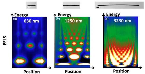
The macroscopic metallic structures support propagation [24], [25] and waveguiding and [26] of the SPP signal, while nanometer scale metallic structures supports LSP resonances whic produce evanescent field, strong confinement [27]. In this thesis, we have used metallic nanostructures which falls in the size range between nanometer scale systems and macroscopic scale system and thus are called micrometer sized metallic structures. The micrometer-sized system combines the characteristics of both SPP and LSP and thus has proven to be a useful candidate for designing plasmonic based optical devices. The micrometric plasmonic structures sustain higher order plasmon modes that have been used in this study to implement different functionalities such as (a) plasmonic transmittance between two selected locations in the system and routing of the plasmonic signal from one location to another, and (b) Boolean logic gate devices. These systems contain higher order plasmonic modes in the visible and near infra red and a new approach is required to describe the modal behaviour of these systems because modes are no more discrete and well separated as in the case of smaller nanoparticles. This can be better understood with the help of figure 2.5 where electron energy loss spectroscopy (EELS) intensity maps recorded over metallic rods of sizes (a) 630nm, (b) 1250nm and (c)
24
3230nm respectively has been displayed. The corresponding SEM images are shown above the EELS maps with scale bars of 200nm each.
Figure 2.5 EELS intensity map measured over metallic nanorods of three different sizes (a) 630nm, (b) 1250nm and (c) 3230nm respectively. The SEM images of the metallic rods are shown above the EELS maps. The scale bars in white are 200nm. [This unpublished work was done previously in collaboration between E. Dujardin and M. Bosman in IMRE Singapore].
In figure 2.5 (a), when the size of the metallic rod is small, the modes are energetically well separated. In this case, the modal behaviour of the metallic rod can be reasonably accounted for by considering dipolar mode and neglecting the two next modes. For the rod of larger dimension in figure 2.5 (b), the modes start appearing closer to each other and for rod of even larger size figure 2.5(c), the modes appear so close to each other that the individual modes are difficult to single out and any optical response will result from contribution of many modes. The modal behaviour of such a system can be better understood in terms of plasmon local density of states (SPLDOS) which provides the modal information inside a given ensemble of nanostructures irrespective of the illumination mode and by taking into account all contributing modes. We discuss in detail about the plasmonic local density of states in the next section.
2.2 Local density of states
Density of states (DOS) is a scalar function, when multiplied with the energy in a given interval gives us the total number of available states in that energy range. For a non-homogenous system, the spatial variation can be taken into account by considering local properties and thus we calculate the local density of states (LDOS) instead. The notion of LDOS thus become very important in case of nanometre scale systems. It is well established
25
fact that the LDOS of both electrons [28] and photons [29] is modified by the presence of a surface. M. F. Crommie in 1993 used a scanning tunnelling microscope (STM) to show that the electronic LDOS inside an iron corral built on a copper (111) surface gives eigenmodes expected for an electron trapped in a 2D round object [30]. This experiment was followed by theoretical explanations [31], [32] including one based on Green function formalism by Crampin and Bryant [31] in which a fully 3D scattering calculation of the electronic standing wave around the iron corral was explained by the authors. The optical analogy of these electronic quantum corrals was proposed by G. Colas des Francs and C. Girard [33]. The authors performed full scattering calculations of the change in electromagnetic LDOS in the near field when moving from a disordered arbitrary geometry to a perfect circular corral. The change of optical LDOS was found to increase significantly above each pad of the corral. The experimental realization was performed on gold nanoparticle arranged in a corral shape on a dielectric surface [34]–[36]. A scanning near-field optical microscope (SNOM) was used to image the projected LDOS which revealed the electric field confinement around the gold corrals for two orthogonal polarizations of the source dipole. This LDOS corresponding to the optical system is termed as photonic LDOS.
In this chapter, we first recall the definition of photonic LDOS. This is followed by the extension of the concept of photonic LDOS to the plasmonic states inside the metallic nanostructure called surface plasmon local density of states (SPLDOS). We then demonstrate how the intensity of the non linear photoluminescence (NPL) signal depends on the plasmonic modes supported by the metallic nanostructures.
2.2.1 Photonics LDOS
The probability of finding the intensity of the electric field associated with photons of energy ′ℏ𝜔′ in an infinitesimal small volume ‘dr’ at a given point ‘r’ is 𝜌(𝒓, 𝜔). The term 𝜌(𝒓, 𝜔) is the photonic LDOS and is the given by -
𝜌(𝒓, 𝜔) = ∑ |𝑬𝑛 𝒏(𝒓, 𝜔𝑛)|2𝛿(𝜔 − 𝜔𝑛) (2.14) where |𝑬𝒏(𝒓, 𝜔𝑛)| is the amplitude of the normalized electromagnetic field associated with the nth electromagnetic mode and is given by –
∫ |𝑬𝒏(𝒓, 𝜔𝑛)|2𝛿𝒓 = 1 (2.15) Photonic LDOS can be computed by GDM based formulism based on calculation of the electric field susceptibility 𝑺(𝒓, 𝒓′, 𝜔). All these electromagnetic modes obey the Helmholtz equation derived from Maxwell’s equation [36] –
26
−∇ × ∇ × 𝑬𝒏(𝒓, 𝜔𝑛) + 𝑘𝑛2𝑬𝒏(𝒓, 𝜔𝑛) = 0 (2.16) and a closure formula –
∑ 𝑬𝑛 𝒏(𝒓, 𝜔𝑛)𝑬𝒏∗(𝒓, 𝜔𝑛)= 𝑰𝛿(𝒓 − 𝒓′) (2.17) where I is the unit dyadic and 𝛿(𝒓 − 𝒓′) is the Dirac delta function which can be represented by
𝛿(𝑥) = − 1
𝜋𝑦→0lim𝐼𝑚( 1
𝑥+𝑖𝑦) (2.18) Using equation (2.18), we can rewrite equation (2.3) as
𝜌(𝒓, 𝜔) = − 1
𝜋𝑦→0lim𝐼𝑚(
|𝑬𝒏(𝒓,𝜔𝑛)|2
𝑘02−𝑘𝑛2+𝑖𝑦) (2.19)
Next, we define the electric field susceptibility of the system, S(r, r’,) similar to equation (2.16)
−∇ × ∇ × 𝑺(𝒓, 𝒓’, 𝜔)+𝑘02𝑺(𝒓, 𝒓’, 𝜔) = −4𝜋𝑘02𝑰𝛿(𝒓 − 𝒓′) (2.20) The closure formula (2.17) can be used here to deduce the spectral representation of the propagator of the system as a function of the |𝑬𝒏(𝒓, 𝜔𝑛)| -
𝑺(𝒓, 𝒓′, 𝜔) = −4𝜋𝑘𝑛2∑ 𝑬𝒏(𝒓,𝜔𝑛)𝑬𝒏∗(𝒓,𝜔𝑛)
𝑘02−𝑘𝑛2
𝑛 (2.21) From equations (2.19) and (2.21), we arrive at following equation –
𝜌(𝒓, 𝜔) = 1 4𝜋𝑘02
𝐼𝑚[𝑇𝑟{𝑺(𝒓, 𝒓′, 𝜔)}] (2.22a) The equation (2.22a) gives the relationship between photonic LDOS and the propagator associated with a metal structure, which is a dyadic tensor containing the whole electromagnetic response of the object. This equation can also be expressed in terms frequency unit, 𝜔 as –
𝜌(𝒓, 𝜔) = 1
2𝜋𝜔2 𝐼𝑚[𝑇𝑟{𝑺(𝒓, 𝒓
′, 𝜔)}] (2.22b) Using this equation (2.22), we can calculate the photonic LDOS as a function of frequency at a
given point of space around the metal structure. This equation also concludes that the photonic LDOS gives us the spectral distribution of different electromagnetic modes irrespective of the characteristics of the illumination field. Figure 2.6(a) presents an example where this technique has been used by C. Girard et. al. [36] to calculate the photonics LDOS maps in a plane parallel to the surface of nanometer sized gold arranged in form of a hexagonal corral at a constant distance of z = 120nm above the structure. The signal modulation inside the hexagonal corral reveals the confined electromagnetic states sustained by the corral. A nice symmetrical image of the hexagonal corral was obtained by using a circularly polarized light. This numerical simulation quantitatively reproduced the experimental map measured by SNOM in the near vicinity of the system (displayed in figure 2.6 (b)).
27
Figure 2.6 SNOM images computed (A) and measured (B) in the vicinity of nanometer- sized gold arranged like a hexagonal corral (image size: 6 μm × 6 μm). The imaging wavelength is λ0 =543nm. [Reference [36]]
2.2.2 Surface plasmon local density of states (SPLDOS)
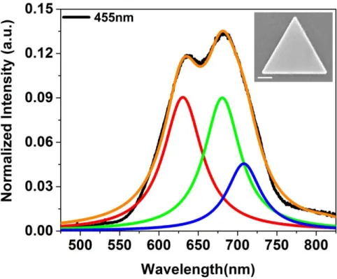
To understand the concept of surface plasmon local density of states, let us consider an example of triangular gold nanoprism. Figure 2.7 (a), (b) and (c) shows the photonic LDOS maps calculated at a plane parallel to the gold nanoprism at Z =100nm, 50nm and 25nm respectively above the prism. For the first map, when Z =100nm, the photonic LDOS consists of non-evanescent complex intensity pattern mostly outside the gold nanoprism. When we decrease the height of the observation plane to Z=50nm, the photonic LDOS pattern starts shrinking. At Z=25nm, it further shrinks and the photonic LDOS which was previously mostly present outside the metallic nanoprism now appears mostly along the outer perimeter and some contrast emerges directly above the nanoprism This implies that as we move closer and closer to the nanostructure there is a significant increase in evanescent states near to the edges of the nanoprism. In figure 2.7 (d), when we go to Z=0nm, the LDOS present in the system is now related to the plasmonic modes inside the metallic nanostructure. At this stage, we would like to introduce an equivalent but distinct concept called surface plasmon local density of states or SPLDOS which are the local density of the states occupied by collective electron oscillations inside a metallic nanostructure. These states govern various properties of metallic nanoparticles like local heat generation, energy loss of a passing by electron, etc. Figure 2.7 (c) in which LDOS has been calculated in near vicinity of the nanoprism appears related to the LDOS map in figure 2.7 (d) but the two maps describe completely different quantities which are photonic LDOS and SPLDOS respectively. Indeed in figure 2.7d, SPLDOS is strictly null out of the structure. SPLDOS can be probed by experimental techniques such as electron energy loss spectroscopy (EELS) and cathodoluminescence [37],. In this work, we have used another very widely used experimental technique called nonlinear photon luminescence microscopy (NPL)
28
to probe SPLDOS inside a metallic nanostructure. NPL is preferred over PL because, as a consequence of nonlinear excitation in NPL, the emission intensity is proportional to nth power of the excitation intensity where n is the number of photons used in multi-photon excitation. This higher luminescence intensity compared to PL, results in better image contrast . In the next section we will establish the relationship between the plasmonic modes supported by the gold nanostructures and nonlinear photon luminescence (NPL).
Figure 2.7 (a), (b) and (c) photonic LDOS maps calculated in three planes (Z=constant) located at Z=100 nm, Z=50 nm, and Z=25 nm above a triangular gold nanoprism. (d) SP–LDOS of the same structure given for comparison. [Reference [38]]
2.2.3 NPL and SPLDOS
To derive a relation between NPL and SPLDOS, we start with considering the standard relation for quantity of energy radiated in a linear process, by an elementary cell of volume ‘r’ positioned at ‘r’ in the nanostructure supported by a transparent substrate and subjected to an illumination field, 𝑬𝒐(𝒓𝟎, 𝒓, 𝜔) position in ‘r0’ –
𝐼(𝒓) = 𝐴𝜒2(𝜔0) |𝑬(𝒓𝟎, 𝒓, 𝜔0)|2𝛿𝒓2 (2.23) where ‘A’ is a real constant and 𝑬(𝒓𝟎, 𝒓, 𝜔0) is the local field induced by the illumination field 𝑬(𝒓𝟎, 𝒓, 𝜔0) and 𝜒(𝜔0) is the linear susceptibility of the nanostructure in vacuum. The dipole induced in the nanostructure by the illumination field is given by –
𝑷𝟎(𝒓, 𝑡) = 𝜒(𝜔0) 𝑬𝟎 (𝒓𝟎, 𝒓, 𝜔0)𝛿𝒓 (2.24) By applying Gauss’ theorem to the oscillating dipole, we can rewrite the equation for radiated energy as [33] -
𝐼(𝒓) = −〈∫ 𝑑𝒓 𝑱(𝒓, 𝑡) 𝑬(𝒓, 𝑡)𝑉 〉 (2.25) where 〈 〉 defines the time average over a period of oscillation, 𝑬(𝒓, 𝑡) denotes the local electric field and 𝑱(𝒓, 𝑡) describe the current density due to the oscillating dipole. Performing Fourier transform on induced current density and local electric field, equation (2.25) can be rewritten as –
29
𝐼(𝒓) = −〈∫ 𝑑𝒓𝑉 ∫−∞∞ 𝑑𝜔 ∫ 𝑑𝜔′∞∞ 𝑱(𝒓, 𝜔). 𝑬(𝒓, 𝜔′) exp[−𝑖(𝜔 + 𝜔′)𝑡]〉 (2.26) Now, since the dipole 𝑷𝟎(𝒓, 𝑡) is induced by the monochromatic illumination field and circularly polarized in XOY plane, it can be written as –
𝑷𝟎(𝒓, 𝑡) = (𝑷𝟎 𝑐𝑜𝑠(𝜔0𝑡), 𝑷𝟎 𝑠𝑖𝑛(𝜔0𝑡), 0) (2.27) and the current density associated with the oscillating dipole can written as –
𝑱(𝒓, 𝜔) = −𝑖𝜔𝑷𝟎(𝒓, 𝜔)𝛿(𝒓′− 𝒓) (2.28) where 𝑷𝟎(𝒓, 𝜔) is the Fourier transform of 𝑷𝟎(𝒓, 𝑡). Now introducing the propagator 𝑺(𝒓, 𝒓𝟎, 𝜔) corresponding to the system which connects the local field to the dipole, we have –
𝑬(𝒓, 𝜔) = 𝑺(𝒓, 𝒓𝟎, 𝜔). 𝑷𝟎(𝒓, 𝜔) (2.29) Then from equation (2.22), (2.24) and (2.25) we have
𝐼(𝒓) = −〈∫−∞∞ 𝑑𝜔∫−∞∞ 𝑑𝜔′𝜔× 𝑷𝟎𝜶(𝒓, 𝜔) 𝑷𝟎𝜷(𝒓, 𝜔′) 𝑺𝜶𝜷(𝒓, 𝒓, 𝜔) exp[−𝑖(𝜔 + 𝜔′)𝑡]〉 (2.30) where (𝛼, 𝛽) = x or y and 𝑃0𝑥(𝜔) = 𝑃0 2 [𝛿(𝜔 − 𝜔0) ± 𝛿(𝜔 + 𝜔0)] and 𝑃0𝑦(𝜔) =𝑃0 2𝑖[𝛿(𝜔 − 𝜔0) ± 𝛿(𝜔 + 𝜔0)] (2.31) After time averaging equation (2.26), we finally obtain –
𝐼(𝒓) = 𝜔0𝑃02
2 𝐼𝑚{𝑆𝑥,𝑥(𝒓, 𝒓, 𝜔0) + 𝑆𝑦,𝑦(𝒓, 𝒓, 𝜔0)} (2.32) Now since the SP-LDOS is given by –
𝜌||(𝒓, 𝜔0) = 1 2𝜋2𝜔
0 𝐼𝑚{𝑆𝑥,𝑥(𝒓, 𝒓, 𝜔0) + 𝑆𝑦,𝑦(𝒓, 𝒓, 𝜔0)} (2.33)
we can rewrite equation (2.32) as –
𝐼(𝒓) = 𝑃02𝜋2𝜔02 𝜌||(𝒓, 𝜔0) (2.34) Now correlating equation (2.23) for energy radiated at position ‘r’ to equation (2.24) and (2.34), we arrive at the equation –
|𝑬(𝒓𝟎, 𝒓, 𝜔)|2 = |𝑬𝟎(𝒓𝟎, 𝒓, 𝜔)|2𝜋2𝜔02𝐴−1𝜌||(𝒓, 𝜔0) (2.35) Equation (2.35) tells us that the local field distribution at a given position ‘r’ is directly proportional to the SPLDOS present at ‘r’. Now the non linear photon luminescence intensity coming out of the metallic nanostructure depends upon the non-linear co-efficient, 𝜂(𝜔0) associated to the metal. In our case, the non-linearity is mostly close to second order
[39]. So we will from now onwards in this work, term the non-linear photoluminescence as two photon luminescence (TPL). The TPL intensity coming out of an elementary cell of volume ‘𝜈’ is thus given by –
30
𝐼𝑇𝑃𝐿(𝒓𝟎, 𝒓, 𝜔) = [ 𝜂(𝜔0). |𝑬(𝒓𝟎, 𝒓, 𝜔)|2]2𝜈 (2.36) Replacing value of |𝑬(𝒓𝟎, 𝒓, 𝜔)|2 from equation (2.35) in to equation (2.36), we get –
𝐼𝑇𝑃𝐿(𝒓𝟎, 𝒓, 𝜔) = 𝜂2(𝜔0)𝜋4𝜔
04𝐴−2∫ |𝑬𝑉 𝟎(𝒓𝟎, 𝒓, 𝜔)|4𝜌2||(𝒓, 𝜔0)𝑑𝒓 (2.37) Equation (2.36) shows us the relationship between TPL signal generated at a point ‘r’ and the existing SPLDOS at the same point ‘r’. It tells us that TPL intensity results from the convolution of squared SPLDOS with the Gaussian beam profile at a given point ‘r’. When the beam waist tends to zero, the TPL maps converge towards the squared-SPLDOS maps. Figure 2.8 shown below has four TPL maps calculated with decreasing beam waist diameter (a) 300nm, (b) 200nm, (c) 100nm and (d) 50 nm respectively. The TPL maps clearly shows that the TPL features depends on the beam waist diameter and as we decrease the beam waist diameter it converges towards SPLDOS map (of figure 2.7fd).
Figure 2.8 TPL maps computed on a gold triangular nanoprism illuminated with a circularly polarized light of beam waist diameter of 300 nm, 200 nm, 100 nm, and 50 nm for (a), (b), (c), (d)) respectively. A SEM image of the object is superimposed to the computed map in (a). [38]
2.3 Single crystalline colloidal system
The exploration of optical characteristics of metallic structures has led to the development of different nanofabrication tools and techniques. All these nanofabrication techniques can be categorized into two parts – top down fabrication approach and bottom up fabrication approach. In this section we briefly discuss the two different nanofabrication approaches, their advantages and shortcomings. We then discuss why the single crystalline colloidal systems are a suitable candidate for the use in plasmonic based devices.
2.3.1 Top down and bottom up approaches
Top-down fabrication is a subtractive process in which material is removed to synthesize nanostructures of desired shapes and sizes. The most common example of the top
31
down fabrication approach is lithography. Lithography consists of a series of fabrication which help in transferring an image from a mask to a substrate. A typical lithographic process has following three steps: (i) coating a substrate with a sensitive precursor material called resist, (ii) exposing the resist to light, electrons or ion beams, (iii) and finally developing the resist image with a suitable chemical, which reveals an image on the substrate. For example, in the case of an electron beam lithography system, nanometer sized focused beam of electrons is used to form a latent image in a layer of resist. This exposure is performed in order to render the resist either more soluble (called a positive tone resist) or less soluble (negative tone resist) in an appropriate developer solution. A desired material is then deposited by physical approach like sputtering or electron beam physical vapour deposition. The left out resist is then etched out of the substrate. Another top down approach, that is widely used for fabrication of nanostructures is focussed ion beam(FIB) milling. In this technique, a focussed ion beam is used to directly mill out a particular structure out of a metallic film. Figure 2.9 (a) shows a silver nanoprism milled out of a silver film by FIB at CEMES. The advantage of the top down approach is the amazing control on the positioning, size and geometry of the fabricated nanostructure. However, the nanostructures fabricated by top down approaches are amorphous in nature, contains granular boundaries and are potentially contaminated by the sputtering atoms or adsorbed resist. These boundaries can be easily seen in the figure 2.9(a). Due to the granular boundaries present on the surface, propagating SPPs scatters in the surface or radiates out of the surface in form of light [17], [40]. This is in addition to the ohmic losses encountered by the conduction electron. Thus scattering through these granular boundaries results in significant SP damping and reduced propagation lengths which leads to limited performance of the plasmonic devices based on the above mentioned fabrication techniques.
The bottom up fabrication on the other hand is an additive process in which atoms are controlled to synthesize different nanostructures like nanowires, nanorods, nanoprisms, etc. Bottom up methods can be divided into gas-phase and liquid-phase methods. In both cases, the nanomaterial is fabricated through a controlled fabrication route that starts from the single atom or molecules. Gas-phase methods include plasma arcing [42] and chemical vapour deposition while sol-gel synthesis [43], [44], colloidal chemistry [45] and molecular self-assembly [46]
are the example of the liquid phase methods. The nanostructures synthesized from bottom up approaches are highly crystalline in nature. Crystalline surface suffers comparatively less scattering related losses and the losses in the nanostructures are limited by the ohmic losses. Figure 2.9(b) shows the SEM images of nanostructures fabricated by colloidal chemistry. We can clearly observe the difference in the crystallinity of the nanostructures fabricated by the
32
two different approaches discussed above. The reduced losses in these highly crystalline nanostructures make them suitable candidates for designing plasmonic based devices.
Figure 2.9 (a)SEM image of silver nanoprism obtained by focussed ion beam milling [41] of 30nm thin Ag film deposited by electron beam physical vapour deposition technique,(b) SEM image of gold nanoprism fabricated by colloidal chemistry
In this work, we have taken advantages of control of geometry from top down approach and high crystallinity from bottom up approach and when necessary, combined the two fabrication approaches to design our nanostructures. In chapter VI and VII, the desired plasmonic devices have been milled out of the highly crystalline gold micro-platelets of size of several of microns by focussed ion beam. This mixed approach has been developed as a tool to design highly efficient plasmonic devices for information transfer and processing related applications.
2.3.2 Crystalline colloidal systems for reconfigurable plasmonic devices
In recent years, there has been abundant scientific literature on interesting plasmonic based devices and information processing prototypes [47]–[50]. The performance of these devices and prototypes however are limited by the scattering losses by the lattice defects and granular boundaries of the system [51]. The increase in imaginary component of the dielectric permittivity of the system results in the damping of SPP signal which further reduce the SPP propagation length and enhancement of the electric field intensity [52], [53]. These limitations in the presently available plasmonic based devices can be overcome by using bottom up strategies. The effort to control shape and size of the nanostructures have led to development of many different chemical synthesis routes for nanorods [54], [55], triangular prisms [56]– [58], nanocubes [59], [60] and many more. These synthesis protocols have gone through continuous improvement over past few decades by gaining a better control over various
33
reaction parameters, homogeneity and the production yield. High crystallinity of the nanostructure produced by the chemical synthesis has led to it use for designing of nanoscale optical interconnects. For example, in a recently reported work by group of M. Kall and N. Hallas, a complete set of basic logic gate operations have been realized using highly crystalline silver nanowires interconnects [61]. The polarization and phase dependent interference between plasmon beams propagating through the wire interconnects were used to realized the logic gate operations. The authors further have proposed more complex logic gates operations and photonic circuits designed by cascading the basic gates. However, the challenge with such kind of interferential devices is the control over positioning of each building block. In addition, cascading of building blocks for realising complex logic gate operations is very difficult because of dissipation in the metallic nanostructures.
These limitations can be overcome by designing plasmonic based devices which can support all complex logic gates operations on single structure. To realize such plasmonic based device, Viarbitskaya et. al. [62] in their work, proposed the use of large 2D Au crystalline nanoprisms which sustain delocalized plasmon modes extending up to micrometre range. The authors have emphasized on the use of SPLDOS as a tool in plasmonic information technology which can be effectively engineered by the control of shape, size and geometry of the gold cavities. This proposal serves as the basis of the designing of the plasmonic based devices in this thesis.
In this work we have used two different gold nanostructures for our studies. The first one is the triangular and hexagonal nanoprisms of size ranging from 300nm to 2m and with a thickness of 202 nm. Spatial properties of these gold cavities and different techniques to tailor and control these properties have been extensively probed by Viarbitskaya et. al. [62], [63] and Cuche et. al. [64]. In this work, these gold cavities will be further probed for understanding of their spectral characteristics in chapter IV. This will be followed by the probing of these gold cavities in a bowtie antenna configuration in chapter V.
Another type of gold nanostructures used in this work has been produced by one pot method (discussed next chapter). These gold nanoparticles are comparatively larger than the previous gold cavities with size ranging from 1 to 20 microns and thickness of 302 nm. These cavities have been used for designing plasmonic cavities of particular shape, size and geometry by focussed ion beam(FIB) milling. These specifically designed resonators with multiple inputs and outputs have been used in this work to realize plasmonic based information processing (chapter VI) and reconfigurable logic gate devices (chapter VII).
34
References:
[1] M. Asghari and A. V. Krishnamoorthy, “Silicon photonics: Energy-efficient communication,” Nat. Photonics, vol. 5, no. 5, pp. 268–270, 2011.
[2] J. Leuthold, C. Koos, and W. Freude, “Nonlinear silicon photonics,” Nat. Photonics, vol. 4, pp. 534–544, 2010.
[3] A. Politi, M. J. Cryan, J. G. Rarity, S. Yu, and J. L. O’Brien, “Silica-on-silicon waveguide quantum circuits.,” Science, vol. 320, no. 5876, pp. 646–9, 2008.
[4] M. Kohnen, M. Succo, P. G. Petrov, R. A. Nyman, M. Trupke, and E. A. Hinds, “An array of integrated atom–photon junctions,” Nat. Photonics, vol. 5, no. 1, pp. 35–38, 2011.
[5] G. Lepert, M. Trupke, M. J. Hartmann, M. B. Plenio, and E. A. Hinds, “Arrays of waveguide-coupled optical cavities that interact strongly with atoms,” New J. Phys., vol. 13, no. 113002, pp. 1–22, 2011. [6] C. Girard, A. Dereux, O. J. F. Martin, and M. Devel, “Importance of confined fields in near-field optical
imaging of subwavelength objects,” Phys. Rev. B, vol. 50, no. 19, pp. 14467–14473, 1994.
[7] W. L. Barnes, A. Dereux, and T. W. Ebbesen, “Surface plasmon subwavelength optics,” Nature, vol. 424, no. 6950, pp. 824–30, 2003.
[8] D. K. Gramotnev and S. I. Bozhevolnyi, “Plasmonics beyond the diffraction limit,” Nat. Photonics, vol. 4, no. 2, pp. 83–91, 2010.
[9] R. W. Wood, “On a Remarkable Case of Uneven Distribution of Light in a Diffraction Grating Spectrum,” Proc. Phys. Soc. London, vol. 18, no. 1, pp. 269–275, 1902.
[10] L. Rayleigh, “On the Dynamical Theory of Gratings,” R. Soc. London, vol. 79, no. 532, pp. 399–416, 1907.
[11] U. Fano, “The Theory of Anomalous Diffraction Gratings and of Quasi-Stationary Waves on Metallic Surfaces (Sommerfeld’s Waves),” J. Opt. Soc. Am., vol. 31, no. 3, p. 213, 1941.
[12] R. H. Ritchie, “Plasma Losses by Fast Electrons in Thin Films,” Phys. Rev., vol. 106, no. 5, pp. 874–881, 1957.
[13] E. Kretschmann and H. Raether, “Radiative Decay of Non Radiative Surface Plasmons Excited by Light,” Zeitschrift fur Naturforschung - Section A Journal of Physical Sciences, vol. 23, no. 12. pp. 2135–2136, 1968.
[14] A. Otto, “Excitation of nonradiative surface plasma waves in silver by the method of frustrated total reflection,” Zeitschrift f??r Phys., vol. 216, no. 4, pp. 398–410, 1968.
[15] S. a Maier, Plasmonics : Fundamentals and Applications, vol. 677, no. 1. 2004.
[16] A. Kocabas, A. Dåna, and A. Aydinli, “Excitation of a surface plasmon with an elastomeric grating,” Appl. Phys. Lett., vol. 89, no. 4, pp. 1–4, 2006.
[17] H. Raether, “Surface Plasmons on Smooth and Rough Surfaces and on Gratings,” Springer Tracts in Modern Physics, vol. 111. p. 136, 1988.
[18] S. Park, G. Lee, S. H. Song, C. H. Oh, and P. S. Kim, “Resonant coupling of surface plasmons to radiation modes by use of dielectric gratings,” Opt. Lett., vol. 28, no. 20, p. 1870, 2003.
[19] B. Hecht, H. Bielefeldt, L. Novotny, Y. Inouye, and D. Pohl, “Local Excitation, Scattering, and Interference of Surface Plasmons,” Phys. Rev. Lett., vol. 77, no. 9, pp. 1889–1892, 1996.
35 886, 2005.
[21] K. Milton and Ernest M. Loebl, The Scattering of Light and Other Electromagnetic Radiation, 1969th ed. Academic Press, 1969.
[22] J. Cao, T. Sun, and K. T. V Grattan, “Gold nanorod-based localized surface plasmon resonance biosensors: A review,” Sensors Actuators, B Chem., vol. 195, pp. 332–351, 2014.
[23] A. Wokaun, J. P. Gordon, and P. F. Liao, “Radiation damping in surface-enhanced Raman scattering,” Phys. Rev. Lett., vol. 48, no. 14, pp. 957–960, 1982.
[24] R. M. Dickson and L. A. Lyon, “Unidirectional plasmon propagation in metallic nanowires,” J. Phys. Chem. B, vol. 104, no. 26, pp. 6095–6098, 2000.
[25] B. Lamprecht et al., “Surface plasmon propagation in microscale metal stripes,” Appl. Phys. Lett., vol. 79, no. 1, pp. 51–53, 2001.
[26] S. Kumar, N. I. Kristiansen, A. Huck, and U. L. Andersen, “Generation and controlled routing of single plasmons on a chip,” Nano Lett., vol. 14, no. 2, pp. 663–669, 2014.
[27] P. Fan et al., “An electrically-driven GaAs nanowire surface plasmon source,” Nano Lett., vol. 12, no. 9, pp. 4943–4947, 2012.
[28] J. Tersoff and D. R. Hamann, “Theory of the scanning tunneling microscope,” Phys. Rev. B, vol. 31, no. 2, pp. 805–813, 1985.
[29] G. S. Agarwal, “Quantum electrodynamics in the presence of dielectrics and conductors. I. Electromagnetic-field response functions and black-body fluctuations in finite geometries,” Phys. Rev. A, vol. 11, no. 1, pp. 230–242, 1975.
[30] M. F. Crommie, C. P. Lutz, and D. M. Eigler, “Confinement of Electrons to Quantum Corrals on a Metal Surface,” Science (80-. )., vol. 262, no. 5131, pp. 218–220, 1993.
[31] S. Crampin, M. H. Boon, and J. E. Inglesfield, “Influence of bulk states on laterally confined surface state electrons,” Phys. Rev. Lett., vol. 73, no. 7, pp. 1015–1018, 1994.
[32] S. Crampin and O. Bryant, “Fully three-dimensional scattering calculations of standing electron waves in quantum nanostructures: The importance of quasiparticle interactions,” Phys. Rev. B, vol. 54, no. 24, pp. R17367–R17370, 1996.
[33] G. Colas des Francs et al., “Optical Analogy to Electronic Quantum Corrals,” Phys. Rev. Lett., vol. 86, no. 21, pp. 4950–4953, 2001.
[34] C. Chicanne et al., “Imaging the Local Density of States of Optical Corrals,” Phys. Rev. Lett., vol. 88, no. 9, p. 97402, 2002.
[35] A. Dereux et al., “Subwavelength mapping of surface photonic states,” Nanotechnology, vol. 14, no. 8, pp. 935–938, 2003.
[36] C. Girard et al., “Imaging surface photonic states with a circularly polarized tip,” Europhys. Lett., vol. 68, no. 6, pp. 797–803, 2004.
[37] A. Losquin and M. Kociak, “Link between Cathodoluminescence and Electron Energy Loss Spectroscopy and the Radiative and Full Electromagnetic Local Density of States,” ACS Photonics, vol. 2, no. 11, pp. 1619–1627, 2015.
[38] S. Viarbitskaya et al., “Tailoring and imaging the plasmonic local density of states in crystalline nanoprisms,” Nat. Mater., vol. 12, no. 5, pp. 426–432, 2013.
![Figure 2.9 (a)SEM image of silver nanoprism obtained by focussed ion beam milling [41] of 30nm thin Ag film deposited by electron beam physical vapour deposition technique, (b) SEM image of gold nanoprism fabricated by colloidal chemistry](https://thumb-eu.123doks.com/thumbv2/123doknet/2114600.8088/32.892.192.700.169.414/nanoprism-deposited-deposition-technique-nanoprism-fabricated-colloidal-chemistry.webp)