HAL Id: hal-02936738
https://hal.archives-ouvertes.fr/hal-02936738
Submitted on 15 Sep 2020
HAL is a multi-disciplinary open access
archive for the deposit and dissemination of
sci-entific research documents, whether they are
pub-lished or not. The documents may come from
teaching and research institutions in France or
abroad, or from public or private research centers.
L’archive ouverte pluridisciplinaire HAL, est
destinée au dépôt et à la diffusion de documents
scientifiques de niveau recherche, publiés ou non,
émanant des établissements d’enseignement et de
recherche français ou étrangers, des laboratoires
publics ou privés.
Design and Development of a Tunable Ferroelectric
Microwave Surface Mounted Device
Caroline Borderon, S. Ginestar, H.W. Gundel, Abdullah Haskou, K. Nadaud,
R. Renoud, A. Sharaiha
To cite this version:
Caroline Borderon, S. Ginestar, H.W. Gundel, Abdullah Haskou, K. Nadaud, et al.. Design and
Development of a Tunable Ferroelectric Microwave Surface Mounted Device. IEEE Transactions on
Ultrasonics, Ferroelectrics and Frequency Control, Institute of Electrical and Electronics Engineers,
2020, 67 (9), pp.1733-1737. �10.1109/TUFFC.2020.2986227�. �hal-02936738�
ACCEPTED MANUSCRIPT
Abstract— Based on a Ba(1-x)SrxTiO3 ferroelectric thin film, a
discrete tunable surface mounted device (SMD) capacitor has been developed for microwave frequency applications purpose. The proposed SMD topology has the particular advantage of inherent decoupling between the RF signal and the DC biasing voltage, necessary to tune the ferroelectric permittivity. The design and technological development of the SMD component is presented and synthesis of the ferroelectric thin film is summarized. Material characterization shows convenient tunability, while low dielectric losses at 10 MHz. Integration of the SMD tunable capacitor into a Planar Inverted-F Antenna has been done in order to evaluate the agility and tunability performance of the antenna.
Index Terms—Ferroelectric devices, Ferroelectric applications,
tunable antenna.
I. INTRODUCTION
HE today's fast and important deployment of connected objects contribute significantly to the development of miniature and agile antennas. In a smart antenna, the volume consumption is greatly reduced as one single resonant element can be used to cover several frequency bands or generate different radiation patterns. High antenna tunability is hence looked for which can be obtained when modifying the antenna electrical length, for example, by insertion of active components such as PIN diodes (positive intrinsic negative diode) [1] or MEMS (micro-electro-mechanical systems) [2]. The tunability can be also obtained by using materials with specific properties controlled by an external stimulus (such as an electric or a magnetic field), like meta-materials [3] or ferromagnetics [4]. Due to the tunability of its permittivity under a DC electric field, the use of ferroelectric materials like potassium tantalate niobate (KTa1-x NbxO3) [5] or barium
strontium titanate (Ba1-xSrxTiO3) [6] can be envisaged, too.
In the present work, we were interested in the design and development of a tunable microwave component which can be integrated as a SMD (Surface Mounted Device) element into a given antenna topology in order to achieve antenna agility. The SMD element has a MIM (metal/insulator/metal) structure
C. Borderon, S. Ginestar, H.W. Gundel and R. Renoud are with IETR UMR CNRS 6164, Université de Nantes, 2 rue de la Houssinière, 44322 Nantes, France
A. Haskou and A. Sharaiha are with IETR UMR CNRS 6164, Université de Rennes 1, 35042 Rennes, France
K. Nadaud is with GREMAN UMR CNRS 7347, Université de Tours, 16 rue Pierre et Marie Curie, 37071 Tours, France
and is based on the perovskite Ba0.80Sr0.20TiO3 (BST)
compound which has a Curie temperature TC = 60 °C [7]. For
the present study, the BST is doped with 1% at. of manganese (Mn2+) which limits the oxygen vacancies in the ferroelectric thin film, thus allowing reduction of the dielectric losses [8].
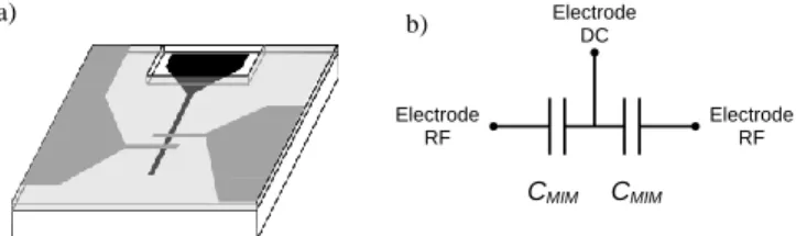
The chosen SMD structure consists of two three-layers MIM capacitors (Fig. 1a). The common bottom electrode (black, Fig. 1a) allows applying the DC bias voltage, necessary to change the polarization state of the ferroelectric thin film (transparent light grey, Fig. 1a) and hence to tune its permittivity. The two coplanar RF top electrodes (grey, Fig. 1a) are designed to be directly inserted into the chosen antenna ground topology and are in series seen from the RF signal (Fig. 2b). The particular advantage of the SMD design is the inherent electrical decoupling between the DC and the RF signal without the need of any additional blocking capacitance, contrary to what has already been reported in the literature [6]. Realization of an SMD component allows easy integration of the tunable capacity into any antenna topology, unlike monolithic integration which is limited due to the high annealing temperature of the ferroelectric material (750 °C), most often not compatible with the antenna fabrication technology process.
In the following we present the realization of the SMD prototype, dielectric characterization of the MIM capacitor (measured between the DC electrode and the RF electrodes), and the example of a Planar Inverted-F Antenna which shall be charged with the SMD element of tunable capacity.
II. EXPERIMENTS
The tunable SMD structure based on the ferroelectric BST thin film was formed on an alumina substrate of 1´´×1´´ surface by successive deposition of the bottom electrode, the BST layer and the top electrode.
The bottom electrode is made of a 40 nm titanium adhesion layer and a platinum film of 300 nm thickness, using radio
Design and development of a tunable
ferroelectric microwave surface mounted device
C. Borderon, S. Ginestar, H.W. Gundel, A. Haskou, K. Nadaud, R. Renoud, A. Sharaiha
T
Fig. 1. Illustration of a) the tunable SMD topology and b) the equivalent electric circuit. Electrode RF Electrode RF Electrode DC a) b) CMIM CMIM
ACCEPTED MANUSCRIPT
This article has been accepted for publication in a future issue of this journal, but has not been fully edited. Content may change prior to final publication. Citation information: DOI 10.1109/TUFFC.2020.2986227, IEEE Transactions on Ultrasonics, Ferroelectrics, and Frequency Control
IEEE Transactions on Ultrasonics, Ferroelectrics, and Frequency Control 2
frequency (RF) magnetron sputtering deposition through a mechanical mask. The pattern of the bottom electrode which consists of a tapered contact pad with a finger shaped electrode of 800 µm length and 35 µm width at its extremity is shown in Fig. 2a.
The deposition of the 1% Mn2+ doped Ba0.80Sr0.20TiO3 film
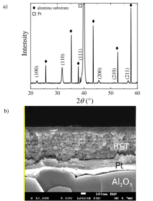
(hereafter denoted BST) was realized by chemical solution deposition. The 1% dopant rate has been found to be optimum [8] for reducing the leakage current, the dielectric losses, and the low frequency charge carrier diffusion in the thin film [8-10]. The precursor solution was composed of barium and strontium acetates to which titanium n-propoxide and an organic stabilizer were mixed in appropriate proportions. Details of the solution preparation are given in [8, 11]. The solution has been deposited on an alumina substrate at 4000 rpm during 20 s and the sample has been annealed during 15 min in a pre-heated open air furnace at 750 °C in order to evaporate the organic material and crystallize the BST film in the ferroelectric perovskite structure (Fig 3a). The BST film does not have a preferential orientation as it can be seen from the X-ray diffraction (XRD) pattern performed with a Brucker
D8 diffractometer using the CuKα radiation but it is well
crystallized and no parasitic peak is visible. Successive
deposition of eight layers results in an overall film thickness of typically 500 nm and in a polycrystalline structure (Fig 3b) [11, 12]. The BST thin film covers the entire surface of the substrate.
Before the deposition of the top electrodes, a via opening to the bottom electrode was created by chemical etching of the BST layer [13]. The mask used for the via, consisting of rectangle of 2 mm length and 900 µm width, is shown in Figure 2b.
The deposition of the top electrodes (copper, 1.2 micron thick), performed by RF-sputtering through a mechanical mask, completes the MIM varactor. The geometry of the two RF electrodes (Fig. 2c) is a tapered contact pad with a finger electrode of 300 µm length and 25 µm width. The two resulting MIM capacitors CMIM have a nominal surface of 875
µm² each.
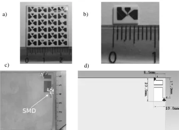
24 SMD elements have been elaborated on one alumina substrate of 1´´×1´´ surface (Fig. 4a) which can be cut out with a diamond saw. The typical SMD dimension is 5 × 3 mm² (Fig. 4b). As an example it is inserted into a Planar Inverted-F Antenna (PIFA) which has been printed on a Rogers duroid
RT5880 substrate (Fig. 4c and 4d). This PIFA antenna
resonance frequency at 2.97 GHz without loading (open circuit) can be tuned in the UHF band by varying the SMD capacitance value. The SMD bottom electrode is connected to the DC bias voltage whereas the two top electrodes are connected to the PIFA antenna ground and are in series for the RF signal.
The final SMD component was examined with an optical microscope (Fig. 5a) which allows verifying high-quality
Fig. 2. Illustration of the different masks used for the elaboration of the ferroelectric SMD: mask for a) the bottom electrode, b) the via opening, and c) the top electrodes.
a) b) 20 30 40 50 60 Pt (21 1) (21 0) (20 0) (11 1) (11 0) Intensit y 2 (°) (10 0) alumina substrate
Fig. 3. a) X-ray diffraction pattern of the elaborated thin film on a platinum coated alumina substrate and b) Cross section SEM micrograph of the deposited BST thin film.
a)
b)
ACCEPTED MANUSCRIPT
This article has been accepted for publication in a future issue of this journal, but has not been fully edited. Content may change prior to final publication. Citation information: DOI 10.1109/TUFFC.2020.2986227, IEEE Transactions on Ultrasonics, Ferroelectrics, and Frequency Control
IEEE Transactions on Ultrasonics, Ferroelectrics, and Frequency Control 3
etching of the BST thin film and deposition of the electrodes. The measured widths of the electrode fingers are approximately 21 µm and 38 µm for the RF and the DC electrode, respectively (Fig. 5b). The resulting MIM capacitor surface of 800 µm² is about 10 % smaller than its nominal value, which is proper to the deposition technique using a mechanical mask and its dimensional tolerances.
In order to determine the dielectric characteristics of the integrated SMD, the capacitance and the dielectric loss factor (tan ) were measured between the DC electrode and the PIFA antenna ground from 100 Hz to 10 MHz using an Agilent 4294A impedance analyzer at 500 mV and the dielectric permittivity of the BST thin film was then calculated. As the two RF electrodes are interconnected via the antenna ground, they are in parallel and the measured capacitance corresponds to 2 CMIM. In order to change the material's polarization state
and hence to determine the permittivity tunability, a DC bias voltage has been superposed to the AC measuring voltage. All the measurements were done at room temperature (20 °C).
III. CHARACTERIZATION RESULTS AND DISCUSSION
Low frequency characterization (< 10 MHz) of the integrated SMD component based on the BST thin film is shown in Fig. 6. A capacitance value 2 CMIM = 4.2 pF and
dielectric losses tan = 0.008 at 10 MHz and 0 V bias have been found. This corresponds to a RF capacitance CMIM of
2.1 pF. Considering the actual dimensions of the MIM structure (surface of 800 µm² and a BST film thickness of 500 nm), a permittivity value of 150 is calculated for the deposited thin film. The capacitance evolution for two applied DC bias voltages is also shown in Fig. 6. A variation from 4.2 pF to 2.4 pF is observed when the DC voltage increases from 0 V to 35 V (at 10 MHz) which corresponds to a tunability of 42.9 %. The tunability nr is defined by:
(0) ( ) (%) 100 (0) r C C V n C (1)
with C(0) and C(V) the capacity without and under the bias voltage V, respectively. The dielectric losses tan at the high frequency side of the measured frequency range are low (tan < 10-2) for 0 V and even under 35 V bias. At low frequency (< 10 kHz) and for 35 V bias, however, the dielectric losses are high due to conduction losses in the electrodes. As this conduction mechanism is not present at the antenna operating frequency (1 GHz), this is not an inconvenient for the using of the SMD variable capacitor.
The dielectric properties of the SMD element at 10 MHz as a function of the voltage are shown in Fig. 7. The C(V) loop presents a butterfly evolution which indicates that the BST
Fig. 4. Photography of a) an alumina substrate with 4×6 SMD components, b) a single SMD, c) the tunable PIFA antenna realized with the ferroelectric SMD and d) the schematic PIFA antenna with the different dimensions.
a) b)
Fig. 5. Photography of the final SMD component showing more particularly a) the via to the bottom electrode and b) the bottom and top electrode fingers separated by the (transparent) BST thin film.
102 103 104 105 106 107 0 1 2 3 4 5 6 Capacity tan 0 V 35 V 0,00 0,05 0,10 0,15 0,20 Capaci ty (pF) tan Fréquency f (Hz)
Fig. 6. Capacity and the dielectric losses tan of the SMD component as a function of the frequency for two DC bias voltages (0V and 35V).
-40 -30 -20 -10 0 10 20 30 40 2.0 2.5 3.0 3.5 4.0 4.5 C a p a c it y ( p F ) Voltage (V) Capacity tan 0.000 0.004 0.008 0.012 0.016 0.020 ta n
Fig. 7. Capacity and the dielectric losses tan of the SMD component as a function of the DC bias voltage at 10 MHz.
c)
c)
a) b)
ACCEPTED MANUSCRIPT
This article has been accepted for publication in a future issue of this journal, but has not been fully edited. Content may change prior to final publication. Citation information: DOI 10.1109/TUFFC.2020.2986227, IEEE Transactions on Ultrasonics, Ferroelectrics, and Frequency Control
IEEE Transactions on Ultrasonics, Ferroelectrics, and Frequency Control 4
thin film is in the ferroelectric state. The asymmetry of the loop is due to the different bottom and top electrode material [15]. It should be noted that low dielectric losses (from 9×10⁻³ to 4×10⁻³ without bias and at 35 V) have been obtained.
In the actual SMD topology, the component's dielectric properties cannot be determined beyond 10 MHz. According to Joncher [14], however, far away from a relaxation, the ferroelectric permittivity and thus the capacity vary following a power law. The capacitance values at high frequencies hence can be deduced by extrapolating the characteristics obtained at low frequencies. The 1 GHz capacity thus has been estimated to 4.06 pF without bias and to 2.35 pF for a DC bias voltage of 35 V, resulting in a tunability of 42%, which is only slightly smaller compared to what has been measured at 10 MHz. At 1 GHz, the dielectric losses should be inferior to the corresponding 10 MHz values and hence below 1×10⁻², too.
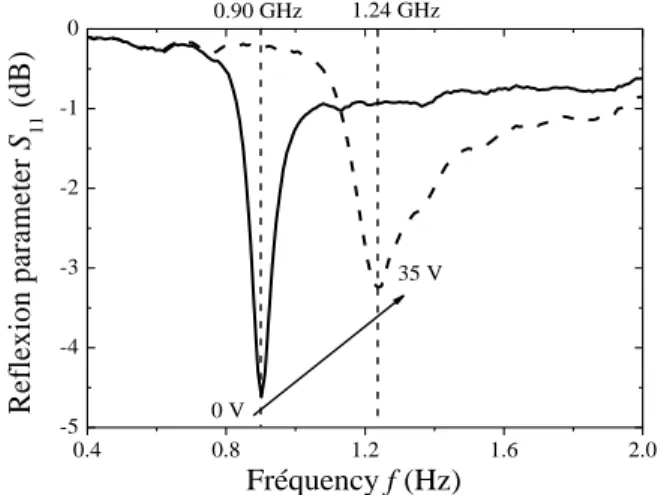
The reflection coefficient of the antenna as a function of the DC voltage applied to the integrated SMD component has been measured using an Agilent E8364B vector network analyzer with an output power of –17dBm. The rf signal is applied via the connector whereas the DC voltage is directly applied between the DC electrode and the ground plane. In Fig. 8 it is shown that the resonant frequency of the antenna prototype shifts from 900 MHz to 1.24 GHz when a DC bias voltage of 35 V is applied. This shift is due to the decrease of the SMD capacity from 4 pF to 2.4 pF. This corresponds to a frequency tuning rate TR of 31.8% which is calculated by:
minmin maxmax
( ) ( ) ( ) ( ) / 2 f C f C TR f C f C (2)
where f(Cmin) and f(Cmax) are the resonant frequencies of the
antenna with respectively the minimum and the maximum capacity values of the SMD (with or without bias). In order to quantify the efficiency of the antenna frequency tunability, a tunability performance () is defined as [6]:
max min TR E
(3)
where Emax and Emin (kV/cm) are the electric bias fields used
for the tuning control of the SMD. Emin is equal to 0 kV/cm
and Emax is related to the maximum bias voltage of 35 V and
corresponds to 700 kV/cm. The resulting tunability performance is 0.045 which is superior of what is reported up to now in the literature [6] for a BST thin film. The tuning rate TR of 31.8 % of the PIFA antenna is comparable to performance on PIFA antenna with commercial varactor diode or RF-MEMS switch [16-18]. The measured reflexion parameter S11 shows also that the radiation efficiency is not
very high compared to HFSS simulation. This is due the dielectric losses of the SMD, especially at 35 V where conduction losses become higher as can be seen in Fig. 6.
IV. CONCLUSION
A discrete tunable surface mounted device capacitor has been developed based on a ferroelectric Ba(1-x)SrxTiO3 thin film
doped with 1% manganese. The particular three-electrodes configuration has been designed in order to obtain inherent decoupling between the DC bias voltage and the RF antenna signal. Easy implementation of the 3x5 mm² SMD element into different antenna topologies hence is possible. Dielectric characterization shows a moderate permittivity tunability of approximately 42% (at 10 MHz, 35 V bias), while rather low dielectric losses (tan = 9×10⁻³ at zero bias and tan = 4×10
-3
at 35 V). For demonstration purpose, the tunable SMD capacitor has been integrated into a Planar Inverted-F Antenna designed for operating in the 1 GHz frequency range. An antenna frequency agility of almost 32% and a tunability performance of 0.045 under 35 V bias have been obtained. Optimization of the electrode configuration, improvement of the material's tunability and further miniaturization of the SMD component is still possible. More generally, integration of the discrete SMD capacity into any adaptive circuit for the development of smart electronic devices may be envisaged.
ACKNOWLEDGMENT
The support of the French National Research Agency (ANR) in the frame of the project SENSAS (Programme INFRA 2013) for part of the work is gratefully acknowledged.
REFERENCES
[1] J-M. Laheurte, “ A switchable CPW-fed slot antenna for multifrequency operation”, Electronics Letters, 2001, vol. 37 (25), pp.1498-1500, 2001. [2] Z. Liu, K. Boyle, J. Krogerus, M.d. Jongh, K. Reimann, R. Kaunisto, J.
Ollikainen, “MEMS-Switched, Frequency-Tunable Hybrid Slot/PIFA”, IEEE Antennas and Wireless Propagation Letters, vol. 8, pp 311-315, 2009.
[3] M.A. Abdalla, Z. Hu, “Compact and tunable metamaterial antenna for multi-band wireless communication applications”, 2011 IEEE International Symposium on Antennas and Propagation (APSURSI), p. 1054-1057 , 2011.
[4] R.K. Mishra, S.S. Pattnaik, N. Das, “Tuning of microstrip antenna on ferrite substrate”, IEEE Transactions on Antennas and Propagation, vol. 41 (2), pp. 230-233, 1993. 0.4 0.8 1.2 1.6 2.0 -5 -4 -3 -2 -1 0 1.24 GHz 35 V R ef le x io n p ar am et er S 11 ( d B ) Fréquency f (Hz) 0 V 0.90 GHz
Fig. 8. Reflexion parameters S11 of the PIFA antenna as the function of frequency for two different DC bias voltages applied to the SMD component.
ACCEPTED MANUSCRIPT
[5] Q. Simon, Y. Corredores, X. Castel, R. Benzerga, R. Sauleau, K. Mahdjoubi, A.L. Febvrier, S. Deputier, M. Guilloux-Viry, L. Zhang, P. Laurent, G. Tanne, “Highly tunable microwave stub resonator on ferroelectric KTa0.5Nb0.5O3 thin film”, vol. 99 (9), pp 092904-3, 2011. [6] H.V. Nguyen, R. Benzerga, C. Borderon, C. Delaveaud, A. Sharaiha, R.
Renoud, C. Le Paven, S. Pavy, K. Nadaud, H.W. Gundel, Materials Research Bulletin 67 2015) 255.
[7] B.A. Baumert, L.-H. Chang, A.T. Matsuda, T.-L. Tsai, C.J. Tracy, R.B. Gregory, P.L. Fejes, N.G. Cave, W. Chen, D.J. Taylor, T. Otsuki, E. Fujii, S. Hayashi, K. Suu, Journal of Applied Physics 82/5 (1997) 2558. [8] K. Nadaud, C. Borderon, R. Renoud, H.W. Gundel, “Effect of manganese
doping of BaSrTiO3 on diffusion and domain wall pinning”, Journal of Applied Physics, vol. 117 (8), pp 084104, 2015.
[9] M.-C. Chiu, Y.-C. Lee, F.-S. Shieu, “Effect of MgO dopant on the microstructure and dielectric properties of rf-sputtered Ba0.5Sr0.5TiO3 thin films”, J Electrochem Soc, vol. 152(11), pp 194-201, 2005..
[10] D. Levasseur, E. Bouyssou, R.D. Paolis, A. Rousseau, F. Coccetti, G. Guegan, S. Payan, M. Maglione, “Systematic tuning of the conduction mechanisms in ferroelectric thin films”, Journal of Physics: Condensed Matter, vol. 25 (49), pp. 495901, 2013..
[11] K. Nadaud, C. Borderon, R. Gillard, E. Fourn, R. Renoud, H.W. Gundel, “Temperature stable BaSrTiO3 thin films suitable for microwave applications”, Thin Solid Films, vol. 591 Part A, pp 90-96, 2015. [12] C. Borderon, “Développement et étude des matériaux ferroélectriques
accordables en vue d’une application pour les antennes intelligentes », PhD Thesis, Université de Nantes, 2008.
[13] S. Pavy, C. Borderon, S. Baron, R. Renoud, H.W. Gundel, “Study of wet chemical etching of BaSrTiO3 ferroelectric thin films for intelligent antenna application”, Journal of Sol-Gel Science and Technology, vol. 74 (2), pp 507-512, 2015.
[14] A.K. Jonscher, “Dielectric relaxation in solids”, Journal of Physics D: Applied Physics, vol. 32 (14), pp. 57-70, 1999.
[15] N. Sama, C. Soyer, D. Remiens, C. Verrue, R. Bouregba, “Bottom and top electrodes nature and PZT film thickness influence on electrical properties”, Sensors and Actuators A: Physical, vol. 158 (1), pp. 99-105, 2010.
[16] Ganesh S., Choukiker Y.K., “Dual band frequency tunable planar inverted-F antenna for mobile handheld devices”, International journal of rf an dmicrowave computer-aided engineering, pp. e22150, 2020. [17] Grigoriev A., Djalilov B, “Tunable antenna for mobile applications”,
2016 IEEE NW Russia Young Researchers in Electricaland Electronic Engineering Conference, pp 408-410, 2016.
[18] Chaabane G, Madrangeas V., Chatras M., Arnaud E., Huitema L., Blondy P., “High-Linearity 3-Bit Frequency-Tunable Planar Inverted-F Antenna for RF Applications”, IEEE Antennas and Wireless Propagation Letters, vol. 16, pp 983-986, 2017