HAL Id: hal-02999474
https://hal.archives-ouvertes.fr/hal-02999474
Submitted on 10 Nov 2020HAL is a multi-disciplinary open access archive for the deposit and dissemination of sci-entific research documents, whether they are pub-lished or not. The documents may come from teaching and research institutions in France or abroad, or from public or private research centers.
L’archive ouverte pluridisciplinaire HAL, est destinée au dépôt et à la diffusion de documents scientifiques de niveau recherche, publiés ou non, émanant des établissements d’enseignement et de recherche français ou étrangers, des laboratoires publics ou privés.
UV nanophotodetector based on a single ZnO:Au
nanowire functionalized with Au-nanoparticles
Vasile Postica, Thierry Pauporte, Bruno Viana, H. Cavers, Mathias Hoppe,
Rainer Adelung, Oleg Lupan
To cite this version:
Vasile Postica, Thierry Pauporte, Bruno Viana, H. Cavers, Mathias Hoppe, et al.. UV nanophotodetec-tor based on a single ZnO:Au nanowire functionalized with Au-nanoparticles. Oxide-based Materials and Devices XI, Feb 2020, San Francisco, France. pp.70, �10.1117/12.2548136�. �hal-02999474�
1 Please cite this article as:
V. Postica,1 Th. Pauporté,2 B. Viana,2 H. Cavers,3 M. Hoppe,3 R. Adelung,3 O. Lupan,1,2,3
UV nanophotodetector based on a single ZnO:Au nanowire functionalized with
Au-nanoparticles
Spie Proceedings Volume 11281, (2020) 112812C DOI:10.1117/12.2548136
1 Center for Nanotechnology and Nanosensors, Department of Microelectronics and Biomedical Engineering, Technical University of Moldova, 168 Stefan cel Mare Blvd., MD-2004, Chisinau, Republic of Moldova E-mail: [email protected]
2 PSL Université, Chimie ParisTech-CNRS, Institut de Recherche de Chimie Paris, UMR8247, 11 rue P. et M. Curie, 75005 Paris, France
3 Functional Nanomaterials, Institute for Materials Science, Kiel University, 24143 Kiel, Germany
ABSTRACT
In this work, an individual nanowire of zinc oxide (ZnO-NW), decorated with gold nanoparticles (Au-NPs/ZnO-NW), was integrated in a nanophotodetector using a dual beam focused electron/ion beam (FIB/SEM) system. Au-NPs/ZnO-NW arrays were synthesized by one-step electrochemical deposition at relative low-temperatures (90 °C). The nanodevice fabricated with a single nanowire Au-NPs/ZnO-NW demonstrated fast detection of UV radiation up to the operating temperature of 120 ºC. The improved UV sensing properties of an individual Au-NPs/ZnO-NW compared to a single, undecorated, ZnO NW was explained based on the formation of Schottky barriers at the Au/ZnO NW interface, which resulted in a much more narrowed conduction channel and a lower dark current. These results prove that high-performance hybrid nanomaterials may possess superior electrical, optical and sensing properties and are of great interest for further fundamental studies.
Keywords: ZnO, nanosensor, methane, UV light, multifunctional.
1. INTRODUCTION
In the past few decades, the ultraviolet (UV) photodetectors based on wide bandgap semiconductor nanowires have been successfully developed and proposed for monitoring of UV light, advanced communications, flame detection, air purification, ozone sensing, leak detection, etc. [1,2,3,4]. In addition, the progress of nanotechnologies has enabled the development of a new generation of photodetectors based on individual micro- and nanostructures of different wide bandgap semiconductors [5,6]. Individual quasi-unidimensional (Q1D) nanostructures are ideal building nano-blocks for development of high-performance photodetectors due to enormous surface-to-volume ratio and possibility to achieve high internal gain [7]. Therefore, integration of individual Q1D nanostructures in nanophotodetectors has attracted an intense attention. For example, Hu et al.
2
obtained an ultrahigh external quantum efficiency of 1.32 × 10⁷ for device based on individual SnO 2 NW with uniform diameter and large surface-to-volume ratio [8]. Fang et al. reported for the first time a new high-performance UV photodetector made of an individual Nb2O5 nanobelt with excellent light selectivity and high external quantum-efficiency [9]. Hu et al. successfully fabricated a novel 1D/1D nanocomposite photodetector based on ZnS/ZnO nanobelt with a wide-range UV-A light photoresponse and fast response speed [10]. Zheng et al. reported a low-dimensional-structure vacuum-ultraviolet-sensitive photodetector based on high-quality AlN micro-/nanowires [11]. Liu et
al. demonstrated the possibility of significant enhancement of the UV sensing performances for
individual ZnO NWs by surface functionalization with Au NPs [12].
Herein, the UV sensing properties of the individual ZnO NWs functionalized with Au NPs (Au-NPs/ZnO-NW) prepared by one-step electrochemical deposition as reported previously [13], is presented. Such important parameters, such as applied bias voltage, and the effect of changing the operating temperature, up to 120 ºC, are investigated in detail. The approach used excludes the necessity of additional technological steps for post-growth surface functionalization of ZnO NWs with noble metal nanoparticles, which was also demonstrated for Pd-modified ZnO nanowires [14], and allow easier fabrication of high-performance nanophotodetectors based on individual surface functionalized nanostructures.
2. MATERIAL SYNTHESIS AND DEVICE STRUCTURES FABRICATION
The synthesis method of Au NPs-functionalized ZnO NW arrays is presented in detail in our previous work [13]. In short, it is based on one-step electrochemical deposition on fluorine doped tin oxide coated glass (FTO) with a resistance of 10 Ω/ , which was used as a working electrode (WE), at relatively low temperature (90 ºC) [15]. The electrolyte solution consists of 0.2 mM ZnCl2, 0.1 M KCl and different concentrations of HAuCl4[13].More details on morphological, structural, chemical and optical properties are presented in our previous work [13]. After deposition, samples were thermally annealed at 250 ºC for 10 h. No additional technological steps for post-growth surface functionalization were performed. However, the structural and morphological investigations demonstrated the presence of gold nanoparticles on the surface of ZnO NWs [13]. Based on individual Au-NPs/ZnO-NWs the nanophotodetectors devices were fabricated using FIB/SEM system following the procedure developed in detail by Lupan et al. [16,17,18]. The electrical measurements and UV sensing investigations were performed as was described in previous works [3,19,20,21]. The applied bias voltage was varied in a range from 1 V to 8 V, in order to investigate the influence of self-heating effect on UV sensing properties, and in order to prove the observed results, the operating temperature was varied from room temperature (RT, 25 ºC) to 120 ºC using the external heater mounted into the stage where the nanophotodetector chip was placed.
3. RESULTS AND DISSCUSIONS
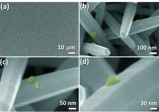
Figure 1(a) shows typical SEM images with top view of Au NPs-functionalized ZnO NW arrays grown for 9000 s on FTO substrate using 2.0 μM of HAuCl4 in electrolyte solution at – 0.65 V vs saturated calomel electrode (SCE). From Figure 1(a) it can be observed that the FTO substrate is fully covered by the dense arrays of Au-NPs/ZnO-NW, which are vertically oriented. The radius of the NWs vary in the 50 – 100 nm range (see Figure 1(b)). The effect of HAuCl4 concentration in electrolyte solution on morphology of nanowires was investigated in our previous work [13]. Figure 1(c,d) clearly
3
shows the presence of Au-NPs on the surface of ZnO NWs. Transmission electron microscopy (TEM) analysis demonstrated that NPs are composed of fcc gold with interplanar distances of d = 0.231 nm and d = 0.201 nm for (1 1 1) and (0 0 2) planes, respectively [13]. The diameter of Au NPs is 10 – 100 nm (see Figure 1(c,d)). The simultaneous growth of ZnO NWs and Au NPs was tentatively explained based on close values between applied bias voltage (– 0.65 V vs SCE) and kinetic regime of gold deposition (– 0.50 V vs SCE) in the case of HAuCl4, as was reported by Wijnhoven et al. [22]. The evidence of Au doping of ZnO NWs, even at higher concentrations of HAuCl4 in electrolyte solution, was not demonstrated using the described investigation methods in our research.
Figure 1. SEM images of Au-modified ZnO nanowire arrays grown using 2.0 μM of HAuCl4 in electrolyte solution at – 0.65 V vs SCE.
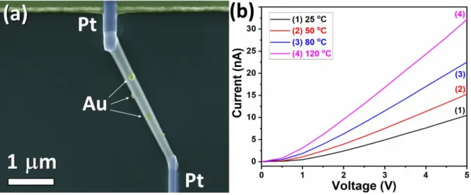
Based on an individual Au NPs-functionalized ZnO NW with radius of ~ 90 nm at one end, the two-terminal nanophotodetector was fabricated. The SEM image of the integrated Au-NPs/ZnO-NW is presented in Figure 2(a). Both ends of the NW were contacted to pre-patterned Au/Cr electrodes on SiO2 (350 nm)/Si substrate using platinum (Pt) complex, as was described previously [23]. The nanophotodetector, fabricated in this work with Pt- Au-NPs/ZnO-NW -Pt structure, demonstrated non-linear current – voltage (I-V) characteristics at room temperature, which indicates the formation of Schottky contacts at both ends of NWs (see Figure 2(b)) [24,25]. The increase in forward current with increasing temperature up to 120 ºC, was observed. The Schottky barrier height (ФBn) and the ideality factor (n) were calculated from the I-V characteristics using the thermionic-emission model for non-ideal Schottky diode [26,27]:
− − = * 2exp exp 1 nkT qV kT q T SA I Bn F (1)
4
where IF is the forward current, S is the area of Schottky contact, A* is the theoretical Richardson’s constant (≈32 A K-2 cm-2 for ZnO [28]), q is the electron charge, k is the Boltzmann’s constant, T is the absolute temperature and V is the applied bias voltage. The values calculated for n at 25, 50, 80 and 120 ºC are ~ 6, ~ 5.2, ~ 4.1, and ~ 2.9, respectively, while the values for ФBn are ~ 0.43, ~ 0.47, ~ 0.49, and ~ 0.52, respectively. The dependence of values on temperature indicates that the electron transport is governed by thermionic emission [29].
Figure 2. (a) SEM image of the nanophotodetector based on an individual Au-NPs/ZnO-NW. (b) Forward current –
voltage characteristics of developed device at different operating temperatures.
Next, the UV sensing properties of the nanophotodetector based on an individual Au-NPs/ZnO-NW is presented. All measurements were performed in air at 20 – 30 % relative humidity. Figure 3(a) shows the dependence of UV response on applied bias voltage (from 1 V to 8 V). The UV response was calculated as the ratio of the measured currents under UV illumination (IUV, λ was 365 nm and light irradiance of about 1 mW/cm2, which was calibrated using the SSEYL Sentry ST-513 UV meter) and dark current (Idark). The highest response, of ~ 7, was obtained at 3 V, while the further increase in the applied bias voltage to 8 V led to a considerable decrease of response to 1.3. According to previous investigations, this can be attributed to self-heating effect of Au-NPs/ZnO-NW [3,30]. Therefore, by increasing the applied bias voltage, rise in local operating temperature and increase in dark current (see Figure 3(b)) are obtained due to Joule heating [3,30]. The increase in operating temperature also increases the probability of recombination of photogenerated e− – h+ pairs, and to the decrease in UV sensing properties, as a result [31]. The dynamic response of individual Au-NPs/ZnO-NW to several exposures of UV illumination at different applied bias voltages is presented in Figure 3(c). The nanophotodetector shows stable electrical baseline without a continuous drift, which is suitable for real applications and does not require additional electrical schemes. In order to evaluate the speed of the nanophotodetector on/off commutation, the rise and decay time constants of the photocurrent were determined through a bi-exponential fit [19]:
− + − + = 1 − 1 1 − 2 ) ( 1 r 2 r t t dark A e A e I t I (2)
5 2 1 4 3 ) ( d d t t dark Ae A e I t I − − + + = (3)
where A1, A2, A3 and A4 are positive constants; τr1, τr2 and τd1, τd2 are the time constants for rising and decaying photocurrent, respectively. The results of fitting are presented in Figure 3(e). The decrease in the values of all the time constants by increasing the bias voltage can be observed from our experimental results.
Figure 3. The dependence of UV response on: (a) applied bias voltage at room temperature; and (b) operating temperature
6
temperature and different operating temperatures; and (d) at different values of operating temperatures for 5 V applied bias voltage. (e) The calculated time constants for rising and decaying photocurrent of individual Au-NPs/ZnO-NW at different bias voltages. (f) Dynamic UV response at 5 V applied bias voltage on nanosensor.
In order to support these assumptions, we performed the UV sensing measurements at different operating temperatures, using an external heater. Figure 3(b) shows the dependence of UV response on operating temperature at the 5 V applied bias voltage. A decrease in the UV response from 3.8 to 1.3 with an increase in temperature from 25 to 120 ºC was observed. The dynamic response of individual Au-NPs/ZnO-NW to several exposures of UV illumination at different operating temperatures is presented in Figure 3(d). It shows an evident increase in dark current and decrease in photocurrent. The multiple exposures to on/off cycles of UV light illumination is presented in Figure 3(f), in order to demonstrate the good stability of the developed nanophotodetector.
Compared to pristine ZnO NW, even with smaller radius (50 nm), reported in a previous work
[32], the UV response of a single Au-NPs/ZnO-NW at 3 V bias voltage is about 6.5 time higher, showing a considerable increase in response value. The enhanced UV response can be explained based on formation of Schottky barriers at the Au/ZnO NW interface due to higher work function of Au (φAu = 5.1 eV) compared to those of ZnO (φAu = 4.1 eV) [12,33]. This will result in a much more narrow conduction channel of Au-NPs/ZnO NW together with a higher modulation of surface electron depletion region after photodesorption of oxygen species, and respectively to a higher UV response. Responsivity (R) and internal photoconductive gain (G) are important parameters of photodetectors and were calculated using the following equations [7]:
G hc q P I R opt ph = = (4) V L G 2e 1 (5)
where Iph is the photocurrent, Popt is the incident optical power of the UV source (~ 1 mW/cm2), η is the quantum efficiency, h is the Planck’s constant, c is the speed of light, λ is the wavelength of UV light (365 nm), L is the interelectrode spacing (~ 2.7 µm), μe is the electron mobility and τ is the photocarrier lifetime. The estimated values for R are 7, 87, 152 and 126 A/W for applied bias voltages of 1, 3, 5 and 8 V, respectively. While the estimated values for G are 2, 25, 45 and 37, respectively. This indicates the occurrence of internal photoconductive gain for fabricated nanophotodetectors, which can be attributed to small interelectrode spacing (see Figure 2(a)) [7,34,35].
5. Conclusions
Herein, we demonstrated the considerable increase in UV detection performances of a nanophotodetector based on a single ZnO nanowire by surface functionalization/modification with Au-NPs. The successful integration of an individual Au-NPs/ZnO nanowire with diameter of 180 nm into nanodevice with good stability using FIB/SEM system was demonstrated. The increase in applied bias voltage up to 8 V, and operating temperature up to 120 ºC demonstrated the considerable decrease in UV response due to the larger probability of recombination of the photogenerated electron-hole pairs. Such nanophotodetectors can be easily integrated into smart devices with low-power consumption for
7
real-time monitoring of UV radiation level, as well as for applications where operating temperature is up to 120 ºC.
Acknowledgements
This research was sponsored in part by the NATO Science for Peace and Security Programme (SPS) under grant G5634 „Advanced Electro-Optical Chemical Sensors” AMOXES. Dr. Lupan gratefully acknowledges PSL University, Chimie-ParisTech for invited professor position in 2018 and 2019, CNRS Council for support as expert scientist at IRCP Chimie ParisTech, Paris. This research was sponsored partially by the German Research Foundation (DFG-Deutsche Forschungsgemeinschaft) under the schemes PAK 902 (SFB1261, FOR2093 & AD 183/16-1) and by Project SFB859.
References
1. Chen, H.; Liu, K.; Hu, L.; Al-Ghamdi, A. A.; Fang, X., New concept ultraviolet photodetectors. Mater.
Today 2015, 18, 493-502
2. Zou, Y.; Zhang, Y.; Hu, Y.; Gu, H., Ultraviolet Detectors Based on Wide Bandgap Semiconductor Nanowire: A Review. Sensors 2018, 18, E2072
3. Lupan, O.; Cretu, V.; Postica, V.; Ahmadi, M.; Cuenya, B. R.; Chow, L.; Tiginyanu, I.; Viana, B.; Pauporté, T.; Adelung, R., Silver-doped zinc oxide single nanowire multifunctional nanosensor with a significant enhancement in response. Sens. Actuators B 2016, 223, 893-903
4. Pauporté, T.; Lupan, O.; Postica, V.; Hoppe, M.; Chow, L.; Adelung, R., Al-Doped ZnO Nanowires by Electrochemical Deposition for Selective VOC Nanosensor and Nanophotodetector. Phys. Status Solidi (a) 2018, 215, 1700824
5. Peng, L.; Hu, L.; Fang, X., Low-Dimensional Nanostructure Ultraviolet Photodetectors. Adv. Mater. 2013, 25, 5321-5328
6. Chen, H.; Liu, H.; Zhang, Z.; Hu, K.; Fang, X., Nanostructured Photodetectors: From Ultraviolet to Terahertz. Adv. Mater. 2016, 28, 403-433
7. Soci, C.; Zhang, A.; Xiang, B.; Dayeh, S. A.; Aplin, D. P. R.; Park, J.; Bao, X. Y.; Lo, Y. H.; Wang, D., ZnO Nanowire UV Photodetectors with High Internal Gain. Nano Lett. 2007, 7, 1003-1009
8. Hu, L.; Yan, J.; Liao, M.; Wu, L.; Fang, X., Ultrahigh External Quantum Efficiency from Thin SnO2
Nanowire Ultraviolet Photodetectors. Small 2011, 7, 1012-1017
9. Fang, X.; Hu, L.; Huo, K.; Gao, B.; Zhao, L.; Liao, M.; Chu, P. K.; Bando, Y.; Golberg, D., New Ultraviolet Photodetector Based on Individual Nb2O5 Nanobelts. Adv. Funct. Mater. 2011, 21, 3907-3915
10. Hu, L.; Yan, J.; Liao, M.; Xiang, H.; Gong, X.; Zhang, L.; Fang, X., An Optimized Ultraviolet-A Light Photodetector with Wide-Range Photoresponse Based on ZnS/ZnO Biaxial Nanobelt. Adv. Mater. 2012, 24, 2305-2309
11. Zheng, W.; Huang, F.; Zheng, R.; Wu, H., Low-Dimensional Structure Vacuum-Ultraviolet-Sensitive (λ < 200 nm) Photodetector with Fast-Response Speed Based on High-Quality AlN Micro/Nanowire. Adv. Mater. 2015, 27, 3921-3927
12. Liu, K.; Sakurai, M.; Liao, M.; Aono, M., Giant Improvement of the Performance of ZnO Nanowire Photodetectors by Au Nanoparticles. J. Phys. Chem. C 2010, 114, 19835-19839
13. Lupan, O.; Postica, V.; Pauporté, T.; Adelung, R., Low-Temperature Solution Synthesis of Au-Modified ZnO Nanowires for Highly Efficient Hydrogen Nanosensors. ACS Appl. Mater. Interfaces2019, 11,
32115−32126
14. Postica, V.; Lupan, O.; Ababii, N.; Hoppe, M.; Adelung, R.; Chow, L.; Sontea, V.; Aschehoug, P.; Viana, V.; Pauporté, T., Detectors based on Pd-doped and PdO-functionalized ZnO nanostructures. SPIE: 2018, Proceedings Volume 10533, Oxide-based Materials and Devices IX; 105332T (2018)
8
15. Lupan, O.; Pauporté, T., Hydrothermal treatment for the marked structural and optical quality improvement of ZnO nanowire arrays deposited on lightweight flexible substrates. J. Cryst. Growth 2010,
312, 2454-2458
16. Lupan, O.; Chai, G.; Chow, L., Fabrication of ZnO nanorod-based hydrogen gas nanosensor.
Microelectron. J. 2007, 38, 1211-1216
17. Lupan, O.; Postica, V.; Adelung, R.; Labat, F.; Ciofini, I.; Schürmann, U.; Kienle, L.; Chow, L.; Viana, B.; Pauporté, T., Functionalized Pd/ZnO Nanowires for Nanosensors. Phys. Status Solidi (RRL) 2017, 12, 1700321 18. Lupan, O.; Postica, V.; Labat, F.; Ciofini, I.; Pauporté, T.; Adelung, R., Ultra-sensitive and selective hydrogen nanosensor with fast response at room temperature based on a single Pd/ZnO nanowire. Sens.
Actuators B 2018, 254, 1259-1270
19. Gedamu, D.; Paulowicz, I.; Kaps, S.; Lupan, O.; Wille, S.; Haidarschin, G.; Mishra Yogendra, K.; Adelung, R., Rapid Fabrication Technique for Interpenetrated ZnO Nanotetrapod Networks for Fast UV Sensors. Adv. Mater. 2013, 26, 1541-1550
20. Postica, V.; Hölken, I.; Schneider, V.; Kaidas, V.; Polonskyi, O.; Cretu, V.; Tiginyanu, I.; Faupel, F.; Adelung, R.; Lupan, O., Multifunctional device based on ZnO:Fe nanostructured films with enhanced UV and ultra-fast ethanol vapour sensing. Mater. Sci. Semicon. Proc. 2016, 49, 20-33
21. Postica, V.; Hoppe, M.; Gröttrup, J.; Hayes, P.; Röbisch, V.; Smazna, D.; Adelung, R.; Viana, B.; Aschehoug, P.; Pauporté, T.; Lupan, O., Morphology dependent UV photoresponse of Sn-doped ZnO microstructures. Solid State Sci. 2017, 71, 75-86
22. Wijnhoven, J. E. G. J.; Zevenhuizen, S. J. M.; Hendriks, M. A.; Vanmaekelbergh, D.; Kelly, J. J.; Vos, W. L., Electrochemical Assembly of Ordered Macropores in Gold. Adv. Mater. 2000, 12, 888-890
23. Lupan, O.; Cretu, V.; Deng, M.; Gedamu, D.; Paulowicz, I.; Kaps, S.; Mishra, Y. K.; Polonskyi, O.; Zamponi, C.; Kienle, L.; Trofim, V.; Tiginyanu, I.; Adelung, R., Versatile Growth of Freestanding Orthorhombic α-Molybdenum Trioxide Nano- and Microstructures by Rapid Thermal Processing for Gas Nanosensors. J.
Phys. Chem. C 2014, 118, 15068-15078
24. Wang, Z. L.; Song, J., Piezoelectric nanogenerators based on zinc oxide nanowire arrays. Science 2006, 312, 242-246
25. Das, S. N.; Moon, K.-J.; Kar, J. P.; Choi, J.-H.; Xiong, J.; Lee, T. I.; Myoung, J.-M., ZnO single nanowire-based UV detectors. Appl. Phys. Lett. 2010, 97, 022103
26. Hu, Y.; Zhou, J.; Yeh, P. H.; Li, Z.; Wei, T. Y.; Wang Zhong, L., Supersensitive, Fast‐Response Nanowire Sensors by Using Schottky Contacts. Adv. Mater. 2010, 22, 3327-3332
27. Cheung, S. K.; Cheung, N. W., Extraction of Schottky diode parameters from forward current‐voltage characteristics. Appl. Phys. Lett. 1986, 49, 85-87
28. Ip, K.; Heo, Y. W.; Baik, K. H.; Norton, D. P.; Pearton, S. J.; Kim, S.; LaRoche, J. R.; Ren, F.,
Temperature-dependent characteristics of Pt Schottky contacts on n-type ZnO. Appl. Phys. Lett. 2004, 84, 2835-2837
29. Suyatin, D. B.; Jain, V.; Nebol’sin, V. A.; Trägårdh, J.; Messing, M. E.; Wagner, J. B.; Persson, O.; Timm, R.; Mikkelsen, A.; Maximov, I.; Samuelson, L.; Pettersson, H., Strong Schottky barrier reduction at
Au-catalyst/GaAs-nanowire interfaces by electric dipole formation and Fermi-level unpinning. Nat. Commun. 2014, 5, 3221
30. Prades, J. D.; Jimenez-Diaz, R.; Hernandez-Ramirez, F.; Barth, S.; Cirera, A.; Romano-Rodriguez, A.; Mathur, S.; Morante, J. R., Ultralow power consumption gas sensors based on self-heated individual nanowires. Appl. Phys. Lett. 2008, 93, 123110
31. Guo, L.; Zhang, H.; Zhao, D.; Li, B.; Zhang, Z.; Jiang, M.; Shen, D., High responsivity ZnO nanowires based UV detector fabricated by the dielectrophoresis method. SEns. ActuatorsB 2012, 166-167, 12-16 32. Lupan, O.; Chai, G.; Chow, L.; Emelchenko, G. A.; Heinrich, H.; Ursaki, V. V.; Gruzintsev, A. N.; Tiginyanu, I. M.; Redkin, A. N., Ultraviolet photoconductive sensor based on single ZnO nanowire. Phys.
Status Solidi A 2010, 207, 1735-1740
33. Joondong, K.; Ju-Hyung, Y.; Chang Hyun, K.; Yun Chang, P.; Ju Yeon, W.; Jeunghee, P.; Jung-Ho, L.; Junsin, Y.; Chang-Soo, H., ZnO nanowire-embedded Schottky diode for effective UV detection by the barrier reduction effect. Nanotechnology 2010, 21, 115205
9
34. Peng, S.-M.; Su, Y.-K.; Ji, L.-W.; Wu, C.-Z.; Cheng, W.-B.; Chao, W.-C., ZnO Nanobridge Array UV Photodetectors. J. Phys. Chem. C 2010, 114, 3204-3208
35. Lupan, O.; Postica, V.; Pauporté, Th.; Viana, B.; Terasa, M-I.; Adelung, R., Room temperature gas nanosensors based on individual and multiple networked Au-modified ZnO nanowires. Sensors & Actuators: