Technology researchers and makes it freely available over the web where possible.
This is an author-deposited version published in: https://sam.ensam.eu
Handle ID: .http://hdl.handle.net/10985/6748
To cite this version :
François GRUSON, Philippe LE MOIGNE, Philippe DELARUE, Arnaud VIDET, Xavier
CIMETIERE, Michel ARPILLIERE - A Simple Carrier-Based Modulation for the SVM of the Matrix Converter - IEEE Transaction on Industrial Informatics p.947-956 - 2013
Any correspondence concerning this service should be sent to the repository Administrator : [email protected]
Abstract - Today, industry has not fully embraced the matrix converter solution. One important reason is its high control complexity. It is therefore relevant to propose a simpler but efficient modulation scheme, similar as three phase VSI modulators with the well-known symmetrical carrier-based ones. The modulation presented in this paper is equivalent to a particular Space Vector Modulation (SVM) and takes into account harmonics and unbalanced input voltages, with the same maximum voltage transfer ratio (86%). The aim of this work is to propose a simple and general pulse-width-modulation method using carrier-based modulator for an easier matrix converter control. Furthermore, a simple duty cycle calculation method is used, based on a virtual matrix converter. Finally, simulations and experimentations are presented to validate this simple, original and efficient modulation concept equivalent to matrix converter SVM.
Index Terms - Matrix converter, power conversion, AC–AC, AC-AC conversion, power converter, pulse-width-modulated power converters, pulse-width modulation, PWM, DPWM.
I. INTRODUCTION
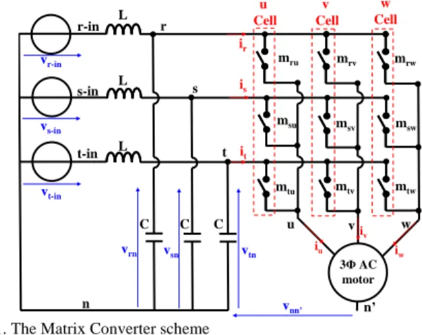
he Matrix Converter, shown in Fig. 1, is a direct three-phase to three-three-phase forced-commuted power converter which directly connects the mains power supply (r, s, t) to the motor (u, v, w) through nine fully controlled bidirectional switches. The input network (r-in, s-in, t-in) is connected to the matrix converter through an L-C input filter as shown in Fig.1. This converter, which can be decomposed in three “cells” as shown in Fig. 1, generates variable frequency and amplitude output voltages (limited to 86% of the input voltage amplitude with over-voltage modulation) with any three-phase electrical network. This converter is able to produce sinusoidal input currents, which limits the volume of the L-C input filter.
Manuscript received November 28, 2011. Acknowledgment: This work is supported in part by the European Union, French state, Région Nord Pas-de-Calais and other part by Schneider Toshiba Inverter Europe (STIE). The Europe involve in the Nord pas-de-Calais region with the European fund for the regional development.
Francois Gruson is with Arts et Metiers ParisTech, L2EP, 8 Bvd Louis XIV, 59046 Lille Cedex (phone: +33(0)3-20-62-22-46; e-mail: [email protected])
Ph. Le Moigne and X.Cimetiere are with the Univ Lille Nord de France, F-59000 Lille, France and Laboratoire d’Electrotechnique et d’Electronique de Puissance (L2EP) of Lille at the Ecole Centrale de Lille (ECLille), BP-48 - 59851 Villeneuve d’Ascq, France (phone: +33(0)3-20-67-60-75; e-mail: [email protected]; [email protected]).
Ph. Delarue and A.Videt are with the Univ Lille Nord de France, F-59000 Lille, France and the Laboratoire d’Electrotechnique et d’Electronique de Puissance (L2EP) of Lille at the Université des sciences et technologie de Lille (USTL), 59655 Villeneuve d’Ascq Cedex, France (e-mail: [email protected], [email protected]).
M. Arpillière is with the Schneider Toshiba Inverter Europe (STIE) Electrical Engineering Department, 27120 Pacy-sur-Eure, France (e-mail: michel.arpilliè[email protected]).
Copyright (c) 2009 IEEE. Personal use of this material is permitted. However, permission to use this material for any other purposes must be obtained from the IEEE by sending a request to [email protected].
This converter has a high power density and a potentially high reliability since electrolytic storage capacitors are not required. Thus, it could become a compact industrial solution for adjustable speed drive applications feeding induction motors.
r s t u n’ w n v mru mrv mrw msu mtu mtv msw mtw msv 3Φ AC motor u Cell ir is it iu iv iw v Cell w Cell vnn’ L L L C C C vr-in vs-in vt-in vrn vsn vtn r-in s-in t-in
Fig. 1. The Matrix Converter scheme
The more useful and interesting modulations are the Space Vector Modulation (SVM) [1]-[4] and the Rectifier and Inverter Vector Modulation (RIV) [5], [6]. These modulations are based on graphical representation methods, duty cycle calculations, and sequenced states application to create the Pulse-Width Modulation (PWM). An 86% voltage ratio (RMS fundamental output voltage divided by the RMS input voltage) is obtained with these methods. In fact, both modulations are equivalent and able to produce sinusoidal output voltages, even when there is unbalance or harmonics in the mains voltages. Since current references of the mains are chosen proportional to the input voltages, input currents are balanced and sinusoidal as long as the mains power supply is a perfect sinusoidal source. A PWM that limits the number of switchings during the modulation period has also been introduced with the SVM representation, using the calculated duty cycles and a defined switching table [7]-[8]. These matrix converter modulations are efficient, but complex to understand, to synthesize compared to the three phase voltage source inverter (VSI) modulations, and thereby heavy to implement in digital processors. The carrier based modulations proposed in the literature are complex to implement into industrial process, by using a discontinuous carrier wave modulator [9], [10] or an asymmetrical one which needs to sum some duty cycles [11],[12].
Hysteresis control methods and Direct Torque Control (DTC) for matrix converter are other interesting alternatives [1],[13],[14]. However, drawbacks still exist such as torque ripple in the low speed region or switching frequency variation according to the change of the motor speed. Thus, industrial applications still focus on controlled-frequency PWM, and especially carrier-based solutions.
Today, industry has not fully embraced the matrix converter solution, mainly due to its high control complexity (modulation, switching control…) and implementation in a digital processor
A Simple Carrier-Based Modulation for the
SVM of the Matrix Converter
F. Gruson, Ph. Le Moigne, Ph. Delarue, A.Videt, X. Cimetière and M. Arpillière.
[15]. It is therefore relevant to propose simple, but efficient modulation schemes like the three phase VSI modulation, with the well-known symmetrical carrier-based modulation. Thus, an interesting scientific and industrial approach is to propose a symmetrical carrier based modulation to greatly simplify this implementation and its understanding.
Moreover, an interesting approach has been introduced by Ishiguro in [16] for the matrix duty cycle calculation, as it limits the number of duty cycle calculations, but it does not propose a satisfying carrier-based modulator.
The aim of this paper is to propose a scalar matrix converter modulation equivalent to the SVM ones in order to obtain the same electrical characteristics (same logic state at each time, same constraints, same efficiency…), with a simple approach. Firstly, this modulation method calculates duty cycles and generates the conversion matrix [M], by using the principle presented in [16] limiting the number of calculations and introducing a virtual matrix converter for better understanding and computing of the matrix modulation. Then, the proposed symmetrical carrier-based PWM, equivalent to the SVM, creates, without any additional calculation, the nine logic control signals of the matrix converter switches by using the matrix [M]. This modulation process can be extended to other PWM strategies.
II. SPACE VECTOR MODULATION (SVM) FOR MATRIX
CONVERTER
In this part, the basic knowledge of the SVM applied to matrix converter is introduced to highlight the proposed modulation objectives. The well-known matrix converter Space Vector Modulation (SVM) [1]-[4] approach leads to define three vector families:
- First family: 6 rotating vectors (each phase input is connected to a different phase output).
- Second family: 3 null vectors (free wheeling ie a switches configuration leading to zero voltage on the load) called Oi with i = 1, 2 or 3.
- Third family (the remaining ones): 18 active vectors called
Aj (with a fixed angular position, and proportional to one input phase-to-phase voltage), where j is an integer between 1 and 18.
Matrix SVM modulations use only the two last families to create output voltages and input currents [17], [18], as the first one has a vector position varying with the time, which is not useful for building the references with the space vector approach.
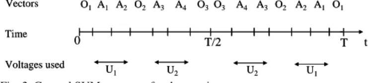
The general matrix SVM sequence, shown in Fig. 2, uses four active vectors Ak (among the six vectors nearest to the
output voltage reference vector), and one to three null states
Ok to complete the PWM period. This specific sequence
allows having only one switching when a vector is changed.
O3 A4 A3 O2 A2 A1 O1 O1 A1 A2 O2 A3 A4 O3 0 T/2 t U2 U2 U1 U1 Voltages used Vectors Time T O3 A4 A3 O2 A2 A1 O1 O1 A1 A2 O2 A3 A4 O3 0 T/2 t U2 U2 U1 U1 Voltages used Vectors Time T
Fig. 2. General SVM sequence for the matrix converter
In classical SVM methods, only the two greatest phase-to-phase input voltages (U1 and U2 in Fig. 2) and also a null
voltage (free-wheeling state) are connected to outputs (u, v, w)
during a PWM period (T) [19]-[21].
The null vector O2 automatically involves at the output the
common potential to U1 and U2, which is in fact the highest
input phase potential in absolute value. A particular modulation can be defined by only using this null state O2, which generates
a discontinuous modulation (DPWM) [19]. This terminology is proposed here, as this specific choice allows blocking one of the three “switching cells” of the matrix converter, in the same way as one inverter leg is blocked when using discontinuous PWM in VSI. This particular modulation, presented in Fig. 3, reduces the number of switching and increases the converter efficiency compared to the general SVM sequence (Fig.2.).
A4 A3 O2 A2 A1 A1 A2 O2 A3 A4 0 T/2 t U2 U1 U1 Voltages used Vectors Time T
Fig. 3. DPWM SVM sequence for the matrix converter To generate this DPWM SVM, it is necessary to
- use the two greatest phase-to-phase input voltages to build the output voltages,
- use only the null state connected to the highest input phase potential in absolute value. In the SVM sequence, this particular null state is necessarily positioned in the medium part of the half PWM period.
The aim of the article is to propose a carrier based modulation method to obtain the SVM DPWM sequence, involving less calculation and thereby a simpler solution compared to the classical SVM implementation.
III. COMPUTING THE DPWM CONVERSION MATRIX [M]
The calculation method of the conversion matrix [M], involving the DPWM and based on a virtual matrix converter concept, is presented in this part.
tw tv tu sw sv su rw rv ru m m m m m m m m m M (1)In order to avoid any short circuit of the input voltage sources and open circuit output currents, the sum of duty cycles for each cell must be equal to 1:
1
sk tk rkm
m
m
, k є u, v, w (2)A. Conversion matrix [M] calculation
A general relation [16] for producing two output phase-to-phase voltages with the three input phase-to-phase-to-phase-to-phase ones is defined in (3). Since the three phase-to-phase voltages are equal to zero, the third output voltage is automatically deducted from (3).
rr rr st st rt rt rs rs uw rr rr st st rt rt rs rs uvu
c
u
c
u
c
u
c
u
u
b
u
b
u
b
u
b
u
(3)bij is a duty cycle that connects uij to uuv. Indirectly, brs controls the 4 switches that can connect r or s to u or v. cij is associated to the output voltage uuw. Since coefficients bij and
cij are duty cycles, they are automatically bounded between zero and one.
With the aim of producing an equivalent modulation to the SVM, only the two largest input phase-to-phase voltages (U1 and U2) must be introduced as explained earlier. In order
to simplify the calculation of the conversion matrix [M], [16] has proposed to calculate the duty cycles of [M] with particular values of input voltages and output voltage references, as shown in Fig. 4. 0.04 0.041 0.042 0.043 0.044 0.045 0.046 0.047 0.048 0.049 0.05 -200 0 200 t (s) In pu t V ol tag es (V ) 0.04 0.041 0.042 0.043 0.044 0.045 0.046 0.047 0.048 0.049 0.05 -200 0 200 t (s) O ut pu t V ol tag es (V ) Vrn Vsn Vtn Vwn' Vvn' Vun' Choice area
Fig. 4. Particular area choice of voltage values to calculate [M]
In this particular time area, urs and urt are the two greatest and positive input phase-to-phase voltages. They are used to create outputs uuv and uuw, which are, in this time range, two positive phase-to-phase voltage references. “u” is the common potential of these two positive references, which will always be connected to “r”, the common potential of the two positive input voltage urs and urt. According to this specific choice, the converter builds the two greatest phase-to-phase output voltage references with the help of the two greatest phase-to-phase input voltages. As a consequence, the highest voltage capability of the converter is necessarily reached in these conditions (voltage ratio equal to 86%).
rr rw rt tw rs sw uw rr rv rt tv rs sv uvu
m
u
m
u
m
u
u
m
u
m
u
m
u
(4) As the output potential “u” is always connected to the input phase “r”, the “u” cell is necessarily blocked.The duty cycles used in equation (4) are defined in (5) and derived from [14], considering that:
- all duty cycles are chosen proportional to the input voltage in order to have input current proportional to the input voltage, as explained in the appendix and in [16], [22]-[23].
- The u cell is blocked.
This way, duty cycles and then the conversion matrix [M] can be defined (5). This solution has the advantage of only requesting the calculation of four duty cycles.
2 st 2 rt 2 rs uw tr st tw 2 st 2 rt 2 rs uv tr st tv tu 2 st 2 rt 2 rs uw st rs sw 2 st 2 rt 2 rs uv st rs sv su tw sw rw tv sv rv ru u u u u ) u u ( m u u u u ) u u ( m 0 m u u u u ) u u ( m u u u u ) u u ( m 0 m m m 1 m m m 1 m 1 m M (5)In the case of asymmetric components and/or harmonics contained in input voltages, the matrix [M] defined in (5)
automatically compensates input voltage disturbances [17]. This propriety will be presented and validated in the simulation of the conversion matrix part (III.C).
B. Matrix-Based Type
The [M] matrix defined in (5) is simple to compute but cannot be used directly for all input and output voltages values. This section defines how this principle can be extended to obtain [M] in any case.
In order to use always the greatest matrix converter input phase-to-phase voltages and to block one of the three switching cells, it is necessary to permanently connect the greatest absolute input voltage to the greatest output voltage with the same sign as the input one, as showed in Fig. 5. This way, the modulation is created by the variation of the two other output potentials which have to be sorted in value and sign (+, 0, 0+, 0-, -), with:
+: highest potential
0: intermediary potential, with a positive value (0+), with a negative value (0-) -: lowest potential + 0 -+ 0 -Input voltage Output voltageTo be created
-U1 U2 + 0 -+ 0 -Input voltage Output voltageTo be created
-U1 U2 -0 + -0 + Input voltage Output voltageTo be created
+
U1
U2
Or
Fig. 5. The 2 possibilities of classified voltage
The choice of the blocked switching cell and of its “ON switch” is dependent on the greatest values of the input voltages (r, s, t) and of the output voltage references (u, v, w), which changes with the time. Two selectors (Fig.6.) have been introduced to realize these inputs and outputs voltage classifications.
In order to be able to use at any time the same matrix-based duty cycle (5), a “virtual matrix converter” (Fig. 6) is introduced with classified input (r’, s’ and t’) and output (u’, v’ and w’) made by both selectors. This virtual converter always has its first virtual cell (u’ cell) blocked as shown in Fig. 6. Consequently, the duty cycle mr’u’ is always equal to 1, and other duty cycles of the first cell (ms’u’ and mt’u’) are always equal to zero.
mr’u’ mr’v’ mr’w’ ms’u’ mt’u’ mt’v’ ms’w’ mt’w’ ms’v’
u’ cell v’ cell w’ cell
s’ t’ u’ v’ w’ Input sel ector Output selector u v w r s t
Virtual Matrix Converter r’ mr’u’ mr’v’ mr’w’ ms’u’ mt’u’ mt’v’ ms’w’ mt’w’ ms’v’
u’ cell v’ cell w’ cell
s’ t’ u’ v’ w’ Input sel ector Output selector u v w r s t
Virtual Matrix Converter r’
Fig. 6. Virtual matrix converter concept with its two selectors
The states of the input selector and of the output selector have to be defined according to the input and output voltage values. Input potential and output reference potential levels
can be classified, with “+” defining the greatest, “-’’ the lowest and “0” the intermediary one. Thus, selectors have been defined with the following principles:
- The aim of the input selector is to connect the two positive and greatest input phase-to-phase voltages to (r’, s’) and (r’,
t’) inputs of the virtual converter. For this, the input potential
with the largest absolute input value (input potential with the opposite sign to the other two) is always connected to r'.
- The output selector connects to u' the output which has the largest voltage reference with the same sign as r' input,
- This modulation method needs to compute, at any moment, the same four duty cycles (ms’v’, ms’w’, mt’v’ and mt’w’), using equation (4) as shown in (6). The two other input potential assignments (s' and t') and the two other output potential assignments (v' and w') are initially arbitrary. The allocation choice of these input and output potentials generates a permutation of the two last rows (for s' and t' assignment) and two last columns (for v' and w' assignment) in the conversion matrix [MVirtual] defined in (6). A choice has been done to be able to determine the conversion matrix [M].
2 ' t ' s 2 ' t ' r 2 ' s ' r ' w ' u ' r ' t ' t ' s ' w ' t 2 ' t ' s 2 ' t ' r 2 ' s ' r ' v ' u ' r ' t ' t ' s ' v ' t ' u ' t 2 ' t ' s 2 ' t ' r 2 ' s ' r ' w ' u ' t ' s ' s ' r ' w ' s 2 ' t ' s 2 ' t ' r 2 ' s ' r ' v ' u ' t ' s ' s ' r ' v ' s ' u ' s ' w ' t ' w ' s ' w ' r ' v ' t ' v ' s ' v ' r ' u ' r Virtual u u u u ) u u ( m u u u u ) u u ( m 0 m u u u u ) u u ( m u u u u ) u u ( m 0 m m m 1 m m m 1 m 1 m M (6)
The final conversion matrix ([M]) is defined by relation (7).
[M]= [M Input Selector]x[M Virtual]x[M Output Selector] (7)
Finally, the conversion matrix [M] is obtained with a lines and columns specific rotation of the virtual converter conversion matrix [M Virtual].
C. Simulations of the conversion matrix
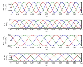
This method for generating the conversion matrix [M] has been implemented in Matlab-Simulink® software. Fig. 7 shows the matrix converter input and output voltages and currents without PWM with a 50-Hz input frequency and maximal voltage input network equal to 325V. The output reference is created with 30Hz and 195V maximal voltage values. The matrix converter operates at 10kVA R-L load with a power factor of 0.86 (4.9Ω; 15.5mH). The 195V at 30Hz voltage applied to this three phases load generates a 34,2A maximum value of the output currents. In order to conserve the input and output active power equality, the maximal input currents should be equal to 17,6A. Fig. 7 validates this modulation approach as the electrical outputs and inputs have the expected values.
0 0.01 0.02 0.03 0.04 0.05 0.06 0.07 0.08 0.09 0.1 -200 0 200 t (s) V rn , V sn , V tn ( V ) 0 0.01 0.02 0.03 0.04 0.05 0.06 0.07 0.08 0.09 0.1 -20 0 20 t (s) Ir , Is , It ( A ) 0 0.01 0.02 0.03 0.04 0.05 0.06 0.07 0.08 0.09 0.1 -200 0 200 t (s) V u n ', V v n ', V w n ' ( V ) 0 0.01 0.02 0.03 0.04 0.05 0.06 0.07 0.08 0.09 0.1 -40 -20 0 20 40 t (s) Iu , I v Iw ( A )
Fig.7. Simulation of the matrix converter with the average model (a) Input network voltages (imposed by the grid) (b) Input network currents generated by the modulation (c) Output voltages generated by the modulation (d) Output currents generated in the R-L load
Fig. 8 shows the u cell duty cycles (mru, msu, mtu). One of these three duty cycle is equal to one and the two others to zero when
vun’ is the largest output reference with the same sign as the largest absolute input voltage, which illustrates the DPWM.
0 0.01 0.02 0.03 0.04 0.05 0.06 0.07 0.08 0.09 0.1 -400 -200 0 200 400 t (s) V rn, V sn, V tn (V ) 0 0.01 0.02 0.03 0.04 0.05 0.06 0.07 0.08 0.09 0.1 -200 0 200 t (s) V un' , V vn' , V w n' (V ) 0 0.01 0.02 0.03 0.04 0.05 0.06 0.07 0.08 0.09 0.1 0 0.5 1 t (s) M ru, M su, M tu Msu Mtu Mru Vun' Vvn' Vwn' Vsn Vtn Vrn msu mtu mru msu , mtu , mru
Fig.8. Simulation of the matrix converter with average model (a) Input network voltages (imposed by the grid) (b) Output voltages generated by the modulation
(d) 3 duty cycle evolution in the “u cell” of the matrix converter This modulation has also been successfully validated by simulation with variable input and output constraints (variations of the frequency, of the input voltages and variable voltage transfer ratio limited to 86%), and under unbalanced/disturbed conditions. Fig.9 shows simulation results of the proposed modulation in this case. One input voltage is increased by 10% and an homopolar component is added in the network voltage (5% of the rms network voltage at 500Hz). The output reference is created with 30Hz and 195V values. The matrix converter operates at 10kVA R-L load with a power factor of 0.86.
0 0.01 0.02 0.03 0.04 0.05 0.06 0.07 0.08 0.09 0.1 -400 -200 0 200 400 t (s) V rn , V sn , V tn ( V ) 0 0.01 0.02 0.03 0.04 0.05 0.06 0.07 0.08 0.09 0.1 -20 0 20 t (s) Ir , Is , It ( A ) 0 0.01 0.02 0.03 0.04 0.05 0.06 0.07 0.08 0.09 0.1 -200 0 200 t (s) V u n ', V v n ', V w n ' ( V ) 0 0.01 0.02 0.03 0.04 0.05 0.06 0.07 0.08 0.09 0.1 -40 -20 0 20 40 t (s) Iu , I v Iw ( A )
Fig.9. Simulation of the matrix converter with the average model in the case of disturbed network
(a) Input network voltages (imposed by the grid) (b) Input network currents generated by the modulation (c) Output voltages generated by the modulation (d) Output currents due to (c) on the R-L load
It generates the same output voltages and consequently the same output current as the balanced ones. Only input currents are modified according to the control principle [16]. Therefore, the proposed matrix calculation of [M], based on the “virtual matrix converter concept”, is validated.
IV. MATRIX CONVERTER PWM MODULATOR
These nine duty cycles (mjk) have to be transformed into logical signals adapted for the control of the nine switches (Sjk), generating the connection matrix [S] (8), with the help of a carrier-based PWM.
tw tv tu sw sv su rw rv ru s s s s s s s s s S (8)A. Carrier Based Switching Cell Modulator.
Each switching cell (u, v, w) is composed of three switches, with only one “ON” switch in each cell at any time (9).
1 S S S 1 S S S 1 S S S tw sw rw tv sv rv tu su ru (9)
With Sij=1 when the switch Sij is ON, Sij=0 when it is OFF. The principle of the modulator, for each switching cell, is to compare one duty cycle to a triangle carrier wave and a second one to this carrier wave complemented to 1. The logic control of the last switch is created by the complement to 1 of the sum of the two previous logic signals as shown in Fig. 10.
Carrier Wave Complement Carrier Wave 1 Sru Ssu= Stu 1 mtu= 0.21 mru= 0.65 Complement To 1 of Sru+Stu
Fig. 10. The based switching cell modulator (ex where Ssu is complemented)
According to this description, the ON switching signal created by the “sum complement to 1” appears automatically in the middle of each slope (Ssu in Fig. 10), and the two other
ON switch signals, at the beginning and the end of the carrier slope (Sru and Stu in Fig. 10).
B. Matrix Converter Carrier-Based Modulator
In order to reproduce the DPWM SVM modulation, each duty cycle of a matrix line must be assigned in “real time”, with the help of “selector concept” (Fig. 6), to the same control allocation (comparison to the carrier wave, to its complement to 1 or equal to the sum of both previous duty cycles complemented to 1). According to “ON signal” positions (Fig. 10), it can be noted that the line complemented to one creates the “ON” state automatically in the “medium part” of each slope, similarly to the position of the null vector
O2 in the DPWM SVM modulation (Fig 3).
The null vector O2 line in the DPWM SVM modulation must
be detected in the conversion matrix [M]. It is necessarily the one with a duty cycle equal to 1 (blocked cell). Then, to the two other lines must be assigned to carriers as shown in Fig. 11. Therefore, the control allocation changes during time (“selector concept”). In example (Fig. 12), the second line has the duty cycle equal to one (msv). Therefore the carriers
control is affected here to the first and third lines. Fig. 12 also illustrates both the active vectors Ak and the null vector O2,
connected here to the “s” input. The second cell (v cell) is blocked (DPWM) and is always connected to the “s” input.
tw tv tu sw sv su rw rv rum
m
m
m
m
m
m
m
m
M
1
1 1Assignment strategy
2 . 0 0 45 . 0 7 . 0 1 2 . 0 1 . 0 0 35 . 0 M 2 . 0 0 45 . 0 7 . 0 1 2 . 0 1 . 0 0 35 . 0 M 1 r s t r s t r s t r s t r s t u v w u v w u v w u v w u v w Equivalent DPWM SVM sequence A1 A2 O2 A3 A4
Fig. 12. Illustration of DPWM modulator and equivalent SVM vector sequence.
This carrier-based modulator is simple to implement and needs only the calculation of the four duty cycles of [M]. It can be applied, with same results, on the virtual converter or on the real matrix converter (fig. 13.) according to the good choice of the line “complemented to one”. The output of modulator is the connexion matrix [S].
PWM [MVirtual] Real Virtual Real Virtual Real Virtual Real Virtual [S] Input voltages Output references
or
PWM [MVirtual] Real Virtual Real Virtual Real Virtual Real Virtual [S] Input voltages Output referencesFig. 13. Carrier wave-based Modulator implementation.
This feature allows making a more flexible modulator and facilitates its implementation in an industrial application.
C. Simulations
This carrier-based modulator has been implemented in Matlab-Simulink® software with the same balanced conditions as in the previous part and with a 10-kHz carrier wave frequency. This modulation technique has been compared to the classical SVM modulation and gives the same value of the connexion matrix [S] for both modulations in each sampling time. Fig. 14 shows the DPWM simulation of the matrix converter. As they are chopped (PWM) and balanced, only one input current (ir) and one output voltage (vun’) are represented to facilitate reading and understanding. As in previous simulations (with the average model), input network parameters are set to 50Hz and 325V, output voltage reference parameters are set to 30Hz and 195V. The matrix converter operates at 10kVA R-L load with a power factor of 0.86.
The motor voltage (vun’), chopped sinusoidal voltage at 30Hz, is presented. It has the expected fundamental RMS value since the three motor currents iu, iv, iw are sinusoidal and balanced with the same RMS value compared to simulations shown in Fig. 7. Input
currents are chopped and in phase with their respective input voltages. As an example here, only ir is presented and its
respective input voltage vrn is shown in continuous bold line.
0 0.01 0.02 0.03 0.04 0.05 0.06 0.07 0.08 0.09 0.1 -200 0 200 t (s) V rn , V sn , V tn ( V ) 0 0.01 0.02 0.03 0.04 0.05 0.06 0.07 0.08 0.09 0.1 -40 -200 20 40 t (s) Ir ( A ) 0 0.01 0.02 0.03 0.04 0.05 0.06 0.07 0.08 0.09 0.1 -400 -200 0 200 400 t (s) V u n ' ( V ) 0 0.01 0.02 0.03 0.04 0.05 0.06 0.07 0.08 0.09 0.1 -40 -200 20 40 t (s) Iu , I v Iw ( A )
Fig.14. Simulation of the matrix converter with the instantaneous model (a) Input network voltages (imposed by the grid)
(b) Input network currents generated by the modulation (c) Output voltages generated by the modulation (d) Output currents generated in the R-L load
Fig. 15 shows simulation results of one output voltage (vun) and the common mode voltage vnn’. The vun voltage illustrates the blocking state (DPWM) of the “u cell” when vun’ is the largest output reference, with the same sign as the largest absolute input voltage.
Fig.15. Simulation of the matrix converter with the instantaneous model
(a) Input network voltages (imposed by the grid) (b)vun (output voltage) generated by the modulation
(c) vn’n (homopolar voltage) induced by the modulation
V. EXPERIMENTATION
A matrix converter prototype as shown in Fig. 16 has been developed with FF200R12KT3_E IGBT and ARCAL2210 driver modules to test this original modulation method, implemented here into a DSP from Texas Instrument (TMS320F2812) and a CPLD from Altera (DB3256-144).
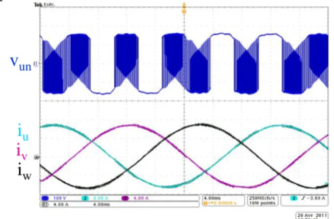
The matrix converter input filter is composed of a 0.6mH inductor, which has a 4.7mΩ internal resistance, and a 10μF capacitor. Experimental results shown in the Fig.17 to Fig.19 have been obtained with an input voltage equal to 120V RMS at 50Hz. The matrix converter has been connected to a three phases R-L load with a 0.63 power factor (R=11.85Ω; L=7.7mH). The ratio q (RMS output voltage divide by the RMS input voltage) is set to 0.8, the output voltage is 96V RMS and the output frequency is defined at 30Hz. The triangle carrier wave frequency has been set to 10 kHz.
For secure commutations, gate transistor signals of Matrix
0 0.01 0.02 0.03 0.04 0.05 0.06 0.07 0.08 0.09 0.1 -400 -200 0 200 400 t (s) V rn , V sn , V tn (V ) 0 0.01 0.02 0.03 0.04 0.05 0.06 0.07 0.08 0.09 0.1 -400 -2000 200 400 t (s) V un (V ) 0 0.01 0.02 0.03 0.04 0.05 0.06 0.07 0.08 0.09 0.1 -400 -200 0 200 400 t (s) V nn ' ( V ) 0 0.01 0.02 0.03 0.04 0.05 0.06 0.07 0.08 0.09 0.1 -400 -2000 200 400 t (s) V un ' ( V )
converter require proper sequences as presented in [4],[24]-[27]. The commutation sequence used in our experiment is either two step current commutation sequences technique or four step voltage commutation sequences ones. A clamp circuit [1],[25] has also been introduced in the matrix converter prototype, as a safety system, in order to prevent any commutation failure.
Fig.16. Matrix converter prototype.
Fig. 17 shows the input voltage vrn and the filtered input current
ir. The input RMS current value is equal to 2.54A for this test. A slight phase shift between voltage and current and a distortion is introduced by the L-C input filter. The harmonic frequency of 2 kHz appearing in the input current is a consequence of the resonance frequency of the input filter [25].
i
r-inv
rnFig.17. Experimental results: Line current (ir-in) and line voltage (vrn)
Fig. 18 shows an output voltage (vun’) and the three load currents (iu, iv, iw). These three load currents are perfectly sinusoidal and balanced (5.1A RMS).
i
vV
un’i
ui
wFig.18. Experimental results: Load currents and vun’ voltage.
As presented in the Fig. 19, the vun voltage exhibits several
none chopped time area. It illustrates the u cell blocking of the matrix converter, which validates the DPWM operation of the proposed modulation method.
i
vv
uni
ui
wFig.19. Experimental results: Load currents and vun voltage.
The input and output power are approximately equal to 925W. These input and output waveform allows validating the operation of the proposed matrix converter modulation.
VI. CONCLUSION
This paper has presented an original carrier-based modulator for matrix converters based on a “virtual matrix converter” concept. The proposed modulation concept is illustrated with the DPWM which blocks one of the three switching cell. This choice limits to four the number of duty cycle calculations. The
proposed carrier-based modulator creates the same
instantaneous connexion matrix [S] as the SVM or the RIV (in the DPWM specific case here), but with less calculation and with a more synthesized and systematic approach. Therefore, this modulation is easier to implement compared to the previous ones and has been patented [28], [29].
Furthermore, the basic modulation concept, illustrated in this paper with the DPWM, can be extended in a simple way to other modulation choices. A future paper will present the general modulation process taking into account the different null states possibilities (freedom degrees) in order to obtain better converter performances (losses, EMC, input currents and output voltages THD….).
Afterwards, it should be an interesting work to compare the efficiency and the electrical characteristics of the proposed modulation methods with the DTC modulation. Then, we should get a global overview of matrix modulation solutions and performances for industry applications.
Finally, the proposed modulation cannot tune the input power factor. In future work, it would be an interesting trend to introduce this parameter in the proposed method to be able to compensate the slight phase shift introduced by the L-C input filter between voltage and current [30] and/or generate reactive power flow for ancillary services in electrical grid (wind turbine applications….).
APPENDIX
The input currents are chosen to be in phase with their respective input voltages. Each input current is proportional to the respective input voltage. The input reactive power must be null as shown in (10). ² v ² v ² v p v v v v v v N i i i tn sn rn tn sn rn tn sn rn t s r (10) We can define (11) by the general matrix Kirchhoff’s laws
tw tv tu sw sv su rw rv ru w v u t s r m m m m m m m m m M with i i i M i i i (11) In this example the ir current is detailed and leads torelation (12). w rw v rv u ru r r tn sn rn rn r i m i m i m i and p ² v ² v ² v v p i (12)
The input power must be equal to the load power since no storage is used on the matrix converter.
w rw v rv u ru w wn v vn u un r r
i
m
i
m
i
m
)
i
v
i
v
i
v
(
i
(13) The easiest solution for the equation (13) is shown in (14)rn wn tn sn rn rn wn r rw rn vn tn sn rn rn vn r rv rn un tn sn rn rn un r ru v K v v v v v v m v K v v v v v v m v K v v v v v v m '' ² ² ² ' ² ² ² ² ² ² (14)
A simple and evident solution to define switches duty cycles is to have proportionality with input voltages. The calculation method [5] uses the phase-to-phase voltage. This proportionality must be verified with the combination switches duty cycles (bij, cij).
st st rt rt rs rs uw st st rt rt rs rs uv u c u c u c u u b u b u b u (15)
The uuv voltage can be decomposed into three input voltages
and switch duty cycles.
rv rn sv sn tv tn
tn tu sn su rn ru uvv
m
v
m
v
m
v
m
v
m
v
m
u
K
'
v
²
K
'
v
²
K
'
v
²
²
v
K
²
v
K
²
v
K
u
tn sn rn tn sn rn uv
K
K
'
v
²
v
²
v
²
u
uv
rn
sn
tn
rs²
st²
tr²
uvu
u
u
u
(16)The easiest solution for equations (15) and (16) is shown in (17).
st st rt rt rs rsu
b
u
b
u
b
and
st st rt rt rs rsu
c
u
c
u
c
(17)It is therefore possible to conclude that switch duty cycles combination (bij, cij) can be proportional to their input
phase-to-phase voltage.
REFERENCES
[1] J. Rodriguez, M. Rivera, J.W. Kolar, P.W. Wheeler, “A Review of Control and Modulation Methods for Matrix Converters,” IEEE Trans. Ind. Electron., vol.59, no.1, pp.58-70, Jan. 2012.
[2] M. Hamouda, H.F. Blanchette, K. Al-Haddad, F.Fnaiech, “An Efficient DSP-FPGA-Based Real-Time implementation method of SVM algorithms for an indirect matrix converter,” IEEE Trans. Ind. Electron., vol.58, no.11, pp.5024-5031, Nov. 2011.
[3] D. Casadei, G. Grandi, G. Serra, and A. Tani, “Space vector control of matrix converters with unity input power factor and sinusoidal input/output waveforms,” in Proc. EPE Conf., Brighton, U.K., Sep. 13– 16, 1993, vol. 7, pp. 170–175.
[4] S. Hongwu et al., “Implementation of voltage-based commutation in space-vector-modulated matrix converter,” IEEE Trans. Ind. Electron., vol.59, no.1, pp.154-166, Jan. 2012.
[5] J.W. Kolar, T. Friedli, J. Rodriguez, P.W. Wheeler, “Review of Three-Phase PWM AC–AC Converter Topologies,” IEEE Trans. Ind. Electron., vol.58, no.11, pp.4988-5006, Nov. 2011.
[6] O. Simon, M. Bruckmann, H. Schierling, J. Mahlein, “Design of pulse patterns for matrix converters”, EPE Journal, vol. 13, No 1, Feb 2003. [7] D. Casadei, G. Serra, A. Tani, L. Zarri, “Matrix converter modulation
strategies: A new general approach based on space-vector representation of the switch state”, IEEE Trans. Ind. Electron., vol. 49, pp. 370-381, April 2002.
[8] H. Hojabri, H. Mokhtari, C. Liuchen, “A Generalized Technique of Modeling, Analysis, and Control of a Matrix Converter Using SVD,” IEEE Trans. Ind. Electron., vol.58, no.3, pp.949-959, March 2011. [9] Y. Young-Doo, S. Seung-Ki, “Carrier-based modulation technique for
matrix converter”, IEEE Trans. Power Electron., Vol. 21, no. 6, pp 1691-1703, Nov 2006.
[10] J. Oyama, T. Xiarong Xia, Higuchi, E. Yamada, T. Koga, “Effect of PWM pulse number on matrix converter characteristics”, In proc. IEEE PESC, 1996, Vol 2, pp 1306-1311.
[11] P.C. Loh, R. Runjie, F. Blaabjerg, W. Peng, “Digital carrier modulation and sampling issues of matrix converters,” IEEE Trans. Power Electron., vol.24, no.7, pp.1690-1700, July 2009.
[12] X. Liu, P. Wang, P. Loh, F. Blaabjerg, “A Three-phase Dual-Input Matrix Converter for Grid Integration of Two AC Type Energy Resources,” IEEE Trans. Ind. Electron., vol.60, no.1, pp.20-30, Jan. 2013.
[13] C. Ortega, A. Arias, C. Caruana, J. Balcells, G.M. Asher, “Improved waveform quality in the direct torque control of matrix-converter-fed PMSM drives,” IEEE Trans. Ind. Electron., vol.57, no.6, pp.2101-2110, June 2010.
[14] M. Rivera, A. Wilson, C. A. Rojas, J. Rodriguez, J. R. Espinoza, P. W. Wheeler, L. Empringham, “A Comparative Assessment of Model Predictive Current Control and Space Vector Modulation in a Direct Matrix Converter, ” Industrial Electronics, IEEE Trans. Ind. Electron., vol.60, no.2, pp. 578-588, Feb. 2013.
[15] E. Monmasson, L. Idkhajine, M.N. Cirstea, I. Bahri, A. Tisan, M.W. Naouar, “FPGAs in Industrial Control Applications, ” IEEE Trans. Ind. Informat., vol. 7, no. 2, pp. 224-243, May 2011.
[16] A. Ishiguro, T. Furuhashi, “A novel control method for forced commutated cycloconverters using instantaneous values of input line-to-line voltages,” IEEE Trans. Ind. Electron., Vol. 38, pp 166-172, No. 3, June 1991.
[17] P. Mutschler, M. Marcks, “A direct control method for matrix converters”, IEEE Trans. Ind. Electron., vol. 49, no. 2, pp. 362-369, April 2002.
[18] P.W. Wheeler, J.C. Clare, M. Apap, K.J. Bradley, "Harmonic loss due to operation of induction machines from matrix converters," IEEE Trans. Ind. Electron., vol.55, no.2, pp.809-816, Feb. 2008.
converter control directly extracted from the matrix converter modulation”, in proc, conf. PCIM Annu. Meeting, 2009, pp 270-276. [20] D. Casadei, G. Serra, A. Tani, L. Zarri, “Optimal use of zero vectors for
minimizing the output current distortion in matrix converters,” IEEE Trans. Ind. Electron., vol.56, no.2, pp.326-336, Feb. 2009.
[21] E. Ormaetxea, J. Andreu, I. Kortabarria, U. Bidarte, I. Mart nez de Alegr a, E. Ibarra, E. Olaguenaga, “Matrix converter protection and computational capabilities based on a system on chip design with an FPGA”, IEEE Trans. Power Electron., vol.26, no.1, pp.272-287, Jan. 2011.
[22] T. Aoki, S. Muroyama, M. Igarashi “A new switched-mode rectifier with sinusoidal input current waveforms” in Proc. IPEC (Tokyo), 1990, p. 755. [23] A. Ishiguro, K. Inagaki, M. Ishida, S. Okuma, Y. Uchikawa, K. Iwata,
“A new method of PWM control for forced commutated cycloconverters using microprocessors,” in Proc. Conf. IEEE IAS Annu. Meeting, 1988, pp. 712–721.
[24] P. Nielsen, F. Blaabjerg, J.K. Pedersen, “New protection issues of a matrix converter: design considerations for adjustable-speed drives,” IEEE Trans. Ind. Appl., vol.35, no.5, pp.1150-1161, Sep 1999. [25] F. Gruson “Modulation naturelle généralisée des convertisseurs
matriciels pour la variation de vitesse,” Ph.D. Dissertation, Dept. Elect. Eng., L2EP-EClille., Lille, France, 2010.
[26] N. Burany, “Safe control of four-quadrant switches,” in Proc. Conf. IEEE IAS Annu. Meeting, San Diego, CA, 1989, pp. 1190–1194. [27] She Hongwu, Lin Hua, He Bi, Wang Xingwei, Yue Limin, An Xing,
“Implementation of Voltage-Based Commutation in Space-Vector-Modulated Matrix Converter,” IEEE Trans. Ind. Electron., vol.59, no.1, pp.154-166, Jan. 2012.
[28] P. Delarue, P. Le Moigne, F. Gruson, P. Baudesson, “Variateur de vitesse de type convertisseur matriciel,” Patent application WO2010069892 (A1), June, 24, 2010.
[29] P. Le Moigne, P. Delarue, F. Gruson, P. Baudesson, “Variateur de vitesse de type convertisseur matriciel,” Patent application WO2010069891 (A1), June, 24, 2010.
[30] H.M. Nguyen, Lee Hong-Hee, Chun Tae-Won, “Input Power Factor Compensation Algorithms Using a New Direct-SVM Method for Matrix Converter,” IEEE Trans. Ind. Electron., vol.58, no.1, pp.232-243, Jan. 2011.
BIOGRAPHIES
François Gruson received the Ph.D. degree in electrical engineering from the Ecole Centrale de Lille, Lille, in 2010. Since 2011, he has been working as Associate Professor at Arts and Metiers ParisTech in the Laboratoire d’Electrotechnique et d’Electronique de Puissance of Lille (L2EP), Lille, France. His research interests include direct AC-AC converter especially matrix converter for adjustable-speed drives, power quality and power electronic converter for electrical grid application.
Philippe Le Moigne (M’93) received the Engineering degree from the Institut Industriel du Nord, Lille, France, in 1986 and the Ph.D. degree in electrical engineering from the University of Lille, in 1990. He is currently a Professor with the Laboratoire d’Electrotechnique et d’Electronique de Puissance, Ecole Centrale de Lille, where he is also the Head of the Power Electronics Department. His major fields of interest include hard switched power converters and supercapacitors, especially the control of multilevel and matrix topologies for medium- and high-power applications with the aim of high power quality and high efficiency.
Philippe Delarue received the Ph.D. degree from the University of Sciences and Technologies of Lille, Villeneuve d’Ascq, France, in 1989. Since 1991, he has been an Assistant Professor with the Polytech’Lille and the Laboratory of Electrotechnics and Power Electronics, Ecole Polytechnique, Universitaire de Lille, Villeneuve d’Ascq. His main research interests include power electronics and multimachine systems.
Arnaud Videt received the Ph.D degree in electrical engineering from the Ecole Centrale de Lille, Lille, France, in 2008. From 2008 to 2010, he has been R&D power electronics engineer with Schneider Toshiba Inverter, Pacy-sur-Eure, France, where his research focused on multilevel inverter control, electromagnetic compatibility, and input power quality for motor drive applications. Since 2010, he has been working as Associate Professor in the Laboratory of Electrical Engineering of Lille (L2EP), Lille, France. His current research interests include power quality, electromagnetic compatibility, and wide- bandgap semiconductor devices for power conversion.
Xavier Cimetière received the Engineering degree from Ecole Centrale de Lille, Lille, France. Since 1992, he has been a Research Engineer with the Laboratoire d’Electrotechnique et d’Electronique de Puissance, Ecole Centrale de Lille, Lille. His research interests include power electronics and the control of electric machines.
Michel Arpilliere was born in Paris, France, in 1952. He received the M.S. degree in physics and math from Paris VII University, Paris, France. He is a Senior Power Electronics Research/Design Engineer in Schneider Electric, a worldwide French company, which is involved in the broad electrical business. He has been working in the Schneider Drive Department for more than 20 years, after several years spent in a small Switch Mode Power Supply (SMPS) company. He is presently “Drive Architect” in Schneider Toshiba Inverter, and a member of the board the European Center of Power Electronic.
![Fig. 4. Particular area choice of voltage values to calculate [M]](https://thumb-eu.123doks.com/thumbv2/123doknet/7432384.219932/4.918.101.418.202.453/fig-particular-area-choice-of-voltage-values-calculate.webp)