HAL Id: tel-01749752
https://pastel.archives-ouvertes.fr/tel-01749752
Submitted on 29 Mar 2018
HAL is a multi-disciplinary open access
archive for the deposit and dissemination of sci-entific research documents, whether they are pub-lished or not. The documents may come from
L’archive ouverte pluridisciplinaire HAL, est destinée au dépôt et à la diffusion de documents scientifiques de niveau recherche, publiés ou non, émanant des établissements d’enseignement et de
plasticity in FCC polycrystals by X-ray synchrotron
topotomography and CPFEM
Nicolas Guéninchault
To cite this version:
Nicolas Guéninchault. Experimental and numerical investigation of incipient plasticity in FCC poly-crystals by X-ray synchrotron topotomography and CPFEM. Mechanics of materials [physics.class-ph]. Université Paris sciences et lettres, 2017. English. �NNT : 2017PSLEM026�. �tel-01749752�
de l’Université de recherche Paris Sciences et Lettres
PSL Research University
Préparée à MINES ParisTech
Experimental and numerical investigation of incipient plasticity in FCC
polycrystals by X-ray synchrotron topotomography and CPFEM
Étude expérimentale et numérique des premiers stades de la plasticité
dans un polycrystal CFC par topotomographie aux rayons X et CPFEM
École doctorale n
o521
SCIENCES ET MÉTIERS DE L’INGÉNIEUR
Spécialité
MÉCANIQUESoutenue par
Nicolas Guéninchault
le 24 Mars 2017
Dirigée par:
Henry Proudhon,
Wolfgang Ludwig,
Samuel Forest.
COMPOSITION DU JURY :Pr. Henning Friis POULSEN
Danmarks Tekniske Universitet ,Rapporteur Pr. Andreas BORBELY
Mines St Étienne, Rapporteur Dr Andrew KING
Synchrotron Soleil, Examinateur Pr. Stéphane BERBENNI
Université de Lorraine, Président Pr. Samuel FOREST
Mines Paristech, Examinateur Pr. Wolfgang LUDWIG
INSA Lyon, Examinateur Dr. Henry PROUDHON
A Elley, Léo, Noah, Baptiste, Clément, Charlie, Stephen et Lisa, avec tout mon amour.
Je tiens à remercier en premier lieu mes encadrants, Henry Proudhon, Samuel Forest et Wolfgang Ludwig. Vous avez su me supporter au fil des années, et avez toujours été présents lorsque j’en avais besoin, ce qui est assez difficile pour être souligné quand on connait vos agendas. Merci à Wolfgang pour m’avoir formé aux techniques expérimentales sur grands instruments, et à toute la famille Lud-wig pour les moments passes à la montagne. Je regrette vraiment de n’avoir pas pu être plus souvent sur ID11. Merci à Samuel, pour sa passion et pour avoir passé un nombre plus que conséquent d’heures avec moi dans le "money time". Cela a vraiment été une chance de travailler avec quelqu’un d’aussi brillant, et nos innombrables discussions m’ont énormément enrichi tant sur le plan scien-tifique que sur le plan personnel. Enfin, merci à Henry. Merci pour m’avoir pris sous ton aile lorsque je n’étais qu’un "jeune" apprenti ingénieur, et d’avoir vu en moi un potentiel « padawan ». Merci d’avoir eu à cœur de me former jour après jour et d’avoir initié mon projet de thèse. La liste des mercis pourrait être très longue, alors simplement merci pour tout. Je me sens vraiment chanceux d’avoir été aux cotés de trois brillants scientifiques, mais aussi de formidables personnes, comme vous.
Merci à Luc Chevalier, pour m’avoir enseigné les bases de la mécanique, mais aussi et surtout pour avoir su m’orienter quand j’en avais besoin. Certaines per-sonnes changent le cours de votre vie, et vous êtes certainement de ceux-là.
Merci à l’école des mines de Paris, MinesParistech, pour le financement de mes travaux, C’est une réelle chance d’avoir eu une liberté totale lors de mes recherches.
Je remercie mon jury, Henning Poulsen et Andras Borbely pour les rappor-teur, Andrew King et Stéphane Berbenni pour les examinateurs. Cela à été un réel honneur d’avoir été adoubé par de telles références dans le domaine de la science des matériaux.
Je remercie aussi mille fois tout le personnel du centre des matériaux avec qui j’ai eu l’occasion de travailler. Une mention spéciale pour René pour s’être rendu disponible et pour sa gentillesse, et à Sylvain et Abdenour pour leur expertise technique, qu’ils ont essayé de me transmettre. Merci aussi à Odile, pour son
aide plus que précieuse lors de mes recherches bibliographiques.
Un grand merci aux thésards du centre avec qui converser et passer du temps a été un plaisir. Et plus particulièrement Quentin, Juan, François, Thibault, Nathan, Clément, Guillaume, Hayat, David, Pierre-Alexis pour les fous rires, les discussions plus ou moins sérieuses et les soirées. Merci aussi à mes compagnons du bureau, Sicong, Arina, Erembert et Jia pour l’aide que vous m’avez apporté.
Je tiens à remercier Erik Lauridsen pour m’avoir fait rejoindre Xnovo Tech-nology, ainsi qu’à toute l’équipe pour l’accueil que vous m’avez réservé. Vous avez su me pousser dans la dernière ligne droite.
Je remercie aussi mes amis de Copenhague, et tout particulièrement Anh, Neil, Mat, Alex, Robin, Carl, Kenth et Anders. Vous m’avez donné de la chaleur et de la force pour terminer la rédaction pendant le terrible hiver danois !
Une grosse dédicace à Xlaw, mes dingos. Merci pour tout, les fous rires, les voyages, les soirées. Merci de m’avoir accueilli au sein de votre famille !
A mes amis les plus "fit", Valérie, Sébastien, Zouzou, Stéphanie, Caroline, Lloyd, Virginie, Yann, Mélanie, Thibault, Florent, Laura, merci pour tout, les rires, les repas, les voyages, tout !
Un grand merci à mes amis de longue date qui ont contribué de près ou de loin à faire de moi ce que je suis aujourd’hui. Teddy, Steward, Émilie, Lionel, Kelly, Damien, les honneurs sont aussi pour vous.
Comment est-il possible de remercier en quelques lignes Auriane et Jackson, qui ont toujours été à mes cotes et ont su trouver les mots lorsque j’en avais besoin ? Merci tout simplement pour votre amour. Vous faites de mois une per-sonne meilleure jour après jour, et je ne serai probablement pas en train d’écrire ces lignes à cette heure-ci sans vous.
Enfin, merci à ma famille. Je pense particulièrement à mon grand-père et Andrée, pour leur soutien, et sans qui je n’aurais pas pu arriver jusque-là. Je ne pourrais jamais vous remercier assez. Et surtout, à ma mère, pour son amour et soutien inconditionnel. Tu es la meilleure, merci infiniment !
Remerciements 3
Abstract 9
Résumé 11
Introduction 13
1 State of the art 17
1.1 Optical microscopy . . . 18
1.2 Electron microscopy . . . 20
1.2.1 Transmission electron microscopy . . . 21
1.2.2 Electron backscattered diffraction . . . 23
1.3 3D X-ray microstructure characterization techniques . . . 25
1.3.1 Laue micro diffraction . . . 25
1.3.2 X-ray microtomography . . . 26
1.3.3 X-ray diffraction topography . . . 28
1.3.4 Three-dimensional X-ray diffraction . . . 33
2 Materials and methods 37 2.1 Introduction . . . 38
2.2 Material . . . 38
2.2.1 Developments of AlLi alloys . . . 38
2.2.2 Effects of Lithium addition to Aluminum . . . 39
2.2.3 Deformation behavior of binary AlLi alloys . . . 40
2.2.4 Conclusion: material used for the study . . . 41
2.3 Methods . . . 42
2.3.1 Diffraction contrast tomography . . . 42
2.3.2 Topotomography . . . 48
2.3.3 Interpretation of the contrast . . . 49
2.4 Nanox . . . 52
3 Experimental 3D observations 63 3.1 Introduction . . . 64
3.1.1 The experimental setup . . . 64
3.1.2 Sequence of the experiment . . . 64
3.1.3 Displacement fields measurements by Digital Volume Correlation (DVC) . . . 68
3.2 Pre-characterization by DCT . . . 69
3.2.1 The three grains cluster . . . 72
3.3 Topography analysis . . . 74
3.3.1 In-situ topography analysis . . . 74
3.4 Topotomography analysis . . . 80
3.4.1 Reconstruction methodology . . . 80
3.4.2 Reconstructed volumes . . . 81
3.4.3 Quality of the reconstruction . . . 83
3.5 Rocking curves . . . 85
3.5.1 2D rocking curves analysis . . . 85
3.5.2 3D rocking curves analysis . . . 86
4 Numerical analysis 91 4.1 Crystal plasticity . . . 92
4.1.1 Continuum crystal plasticity theory . . . 92
4.1.2 Lattice rotations . . . 93
4.1.3 Lattice curvature and the dislocation density tensor . . . 94
4.1.4 Hardening rule . . . 97
4.2 Identification . . . 97
4.2.1 Mechanical testing on macroscopic samples . . . 98
4.2.2 Identification with an homogenized behavior . . . 100
4.3 3D mesh . . . 101
4.3.1 Meshing polycrystals from DCT data . . . 101
4.3.2 Meshing strategy . . . 101
4.3.3 Results: Comparisons with the experimental DCT data . 104 4.4 CPFEM computations . . . 104
4.4.1 Computations methodology . . . 104
4.4.2 Results . . . 106
4.5 Simulation of diffraction . . . 111
4.5.1 Definitions . . . 111
4.5.2 Geometric principles of diffraction in 3D . . . 115
4.5.3 Generating 3D rocking curves . . . 119
4.6.1 Rocking curves . . . 127
4.6.2 Misorientation surfaces . . . 128
4.6.3 Comparative effects of B and Re . . . 128
4.6.4 Comparison with the experimental data . . . 128
Conclusion and outlook 133 Bibliography 138 A Continuum crystal plasticity theory 163 A.1 Thermomechanics of single crystal behaviour . . . 164
A.1.1 Balance equations . . . 164
A.1.2 Kinematics of single crystals . . . 165
A.1.3 Constitutive equations . . . 167
A.1.4 Lattice rotation . . . 169
A.2 The dislocation density tensor . . . 171
A.2.1 Elements of tensor analysis . . . 171
A.2.2 Dislocation density tensor . . . 173
A.2.3 Lattice curvature . . . 174
A.3 Strain gradient plasticity: The “curlHp” model . . . . 176
A.3.1 Balance equations . . . 176
A.3.2 Energy and entropy principles, constitutive equations . 177 A.3.3 Application of the “curlHp” model to a single slip problem 178 A.4 Conclusions . . . 179
B Solving the trigonometric equationA cos(x) + B sin(x) = C 181 C Band profile analysis 183 C.1 Grain 4 . . . 184
C.2 Grain 10 . . . 186
C.2.1 In situ analysis for the primary slip system . . . 186
C.2.2 Secondary slip system . . . 188
Understanding the intimate details of plastic deformation in polycrystalline ma-terials is an important issue to improve material design and ultimately produce safer structural parts with less impact on the environment. This understanding is presently limited by our ability to observe both the microstructure of the mate-rial and the deformation processes in three dimensions (3D) at small length scales and inform mechanical simulations with physical deformation mechanisms of the crystal lattice. Considerable progress has been made in the last decade with surface observation (eg EBSD coupled to digital image correlation) which led to numerous studies combining experimental observations and simulations from the surface microstructure. However, an accurate comparison without knowing the underlying microstructure remain challenging. In this work, we propose a new methodology which allows a quantitative comparison between the obser-vation of deformation mechanisms, the evolution of the grain lattice curvature and the simulated mechanical fields.
For that purpose, a mechanical stress rig dedicated for synchrotron 4D diffraction imaging experiments has been designed, and used to deform an Aluminium-Lithium specimen under tension. The 3D grain map has been ob-tained by diffraction contrast tomography analysis, and a cluster of three grains within the bulk has been selected to be the region of interest of the 4D observa-tion by X-ray topotomography. The appearance and evoluobserva-tion of 3D crystalline defects as a function of the applied load has been observed to be located along well defined crystallographic planes. All three grains showed plastic activity on along two different set of planes, which is not always coherent with a macro-scopic Schmid Factor analysis. The change of the amplitude and the orientation of the average grain curvature has been measured with an unprecedented level of detail by means of 3D rocking curve analysis.
In parallel, crystal plasticity finite element (CPFE) simulations have been car-ried using the 3D grain map measured experimentally. Tension loading was ap-plied to reproduce the experiment numerically and compare the plastic activity on a grain by grain basis. The slip system activity predicted by the model matches in most cases the observed two slip system scenario. A mathematical framework
to predict the local Bragg angle based on the stretch and rotation of the crystal lattice by the elastic strain tensor was derived. Post-processing the intragranu-lar strains fields from the CPFE results allowed to simulate 3D rocking curves, showing excellent agreement with the experimental measurements. This result confirms that in situ X-ray topotomography is a promising tool to study the early stage of polycrystal plasticity within the bulk of millimetric material specimens.
La compréhension des mécanismes de déformation dans les matériaux poly-cristallins est un problème important, qui conditionne notre capacité à concevoir et à produire des pièces de structure plus sures et avec un impact environnemen-tal moindre. Cette compréhension est aujourd’hui limitée par notre capacité à ob-server à la fois la microstructure du matériau et ses mécanismes de déformation en trois dimensions (3D) aux petites échelles, et à informer les simulations mé-caniques à partir des mécanismes physique de déformations du réseau cristallin. Des progrès considérables ont été faits dans les dernières décennies avec les ob-servations de surfaces (i.e. technique EBSD associée a de la corrélation d’image) qui a permis de nombreuses études combinant des observations expérimentales à des simulations, à partir de la surface de la microstructure. Cependant, une comparaison précise sans connaitre la microstructure sous-jacente reste un défi. Dans ce travail, nous proposons une nouvelle méthodologie basée d’une part sur des mesures couplant la tomographie et la diffraction des rayons X, et d’autre part sur des simulations mécaniques de platicité cristalline. Cette approche permet une comparaison quantitative en volume entre les mécanismes de déformation, l’évolution de la courbure du réseau cristallin et les champs mécaniques simulés. Pour ce faire, une machine de traction dédiée aux expériences 4D d’imagerie par diffraction sur grands instruments a été conçue, et utilisée pour déformer en tension un échantillon d’Aluminium Lithium. La cartographie 3D de la mi-crostructure a été obtenue par tomographie par contraste de diffraction, et un agrégat de trois grains dans le volume de l’échantillon a été choisi comme ré-gion d’intérêt pour des observation 4D par topotomographie. L’apparition des premières bandes de glissement en volume et leur évolution au cours du charge-ment ont été observées le long de plans cristallographiques bien définis. Les trois grains ont montré une activité plastique le long de deux familles de plans différents, pas toujours en accord avec une analyse macroscopique du facteur de Schmid, ce qui est attribué à l’influence du voisinage sur l’activation des sys-tèmes de glissement. Les changements d’amplitude et d’orientation de la cour-bure moyenne des grains ont été mesures avec un niveau de détail sans précédent, par une analyse tridimensionnelle des courbes de reflexions.
En parallèle, des simulations de la plasticité cristalline par éléments finis (CPFE) ont été menées utilisant la cartographie tridimensionnelle de la mi-crostructure mesurée expérimentalement. Un chargement uniaxial de traction a été applique pour reproduire numériquement l’expérience, et comparer grain par grain l’activité plastique. L’activité des systèmes de glissement prédite par le modèle est conforme aux observations expérimentales d’une activité plastique le long de deux plans. Un cadre mathématique pour prédire l’angle de Bragg local en fonction des déformations et des rotations du réseau cristallin a été for-mulé. Un post-traitement des champs intragranulaires de déformation à partir des résultats des simulations CPFE a montré une excellente concordance avec les résultats expérimentaux. Ce résultat confirme que la topotomographie in-situ aux rayons X est un outil prometteur pour l’étude des premiers stades de la plasticité cristalline en volume.
Les matériaux polycristallins composent une grande partie des pièces de structure des moyens de transport modernes ou de production d’énergie. Il est dont impor-tant de disposer des connaissances nécessaires a la conception de ces dernières. L’arrangement spatial, la forme, l’orientation des différents cristaux (grains) qui le compose le polycristal influe grandement sur les propriétés mécaniques du matériau. Les mécanismes de plasticité dans ces matériaux sont spécifiques, et la déforma-tion plastique se produit par le mouvement des dislocadéforma-tions. Souvent, ces défauts s’organisent en structures, comme des bandes de glissement.
Les récents progrès des techniques expérimentales on permettent aujourd’hui d’observer les défauts individuellement ou les structures de dislocations, en 2D, 3D, ou 4D. Ces observations peuvent être utilisées comme données d’entrée pour des simulations du comportement mécanique du matériau, et des modèles prenant en compte les mécanismes particuliers de la déformation plastiques dans les cristaux permettent de prédire les champs locaux de contrainte et de déformation, ainsi que l’orientation locale du cristal ainsi que les paramètres de mailles. Comparer ces études 4D et les simulations reste un défi, mais apparait comme une voie promet-teuse pour améliorer notre compréhension des mécanismes de déformations et nos modèles.
Le premier chapitre de ce travail s’attache a faire une revue des différentes tech-niques d’analyses de la microstructure des matériaux actuelles. Le second chapitre expose les caractéristiques du matériau utilise dans le cadre de cette étude, ainsi que les techniques expérimentales utilisées. Le troisième chapitre détaille une expérience originale menée a l’ESRF, qui a permis d’observer en trois dimension l’apparition et l’évolution de défauts cristallins dans trois différents grains. Enfin, une simulation numérique du comportement mécanique de l’échantillon étudié expérimentalement est menée. à la fois expérimentalement ou numériquement.
As early as prehistoric times, human being have shaped stones to make weapons, and be able to hunt. Now, we are capable to confine a 5 million de-grees plasma in the Tokamak toroidal chamber. We constantly use materials with shapes and applications more and more complex. Materials have evolved with mankind through history, when they were not the factor that took a civilization to the next one, as shown by ages of civilization named after materials.
Among these materials, metals had a special place in History and they were the vector of modernity for several civilizations. The development of metallurgy and the industry of bronze ∼ 8000 years b.c. has been the starting point of deep upheaval of the socio-economic world. In the XIXe century, the industrial
rev-olution has been permitted by the new capabilities in terms of production and machining of steel. Since then, metals have been the most widely used compo-nents in structures for the modern ways of of transportation, energy production and construction. Precious metals, integrated in the most recent micro-electronic systems, were part of the transformation of our world into a society of informa-tion. By their inner structure, metallic materials are very specific. The atomic arrangement is both long range and short range ordered, which gives them very interesting physical (mechanical, electrical, etc.) properties. The use of this class of interestingly materials are dictated by the defect structures. Particular applica-tions require a high crystal purity, like Nickel based superalloys monocrystalline turbine blades used in modern jet turbines, decreasing the amount of creep in high temperature applications. Others use defects to produce specific effects, like Ni-Ti shape memory alloys (SMAs) using the reversible movement of twins, allowing to produce self-expanding stents. Understanding how these defects are generated, move, and interact is essential to better predict the life cycle of struc-tural part (improving safety and reducing the ecological impact) or to optimize the performance linked to a specific use. Therefore, it is important to be able to understand and model the behavior of crystalline materials based on the physical mechanisms of deformation.
In polycrystalline materials, the microstructure composed by the grain shapes, orientations, sizes and spatial arrangement, controls the macroscopic properties such as the yield stress. The plastic deformation by dislocation motion is the principal deformation mechanism and lead to the formation of defects in the crystal structure. Crystal slip is often observed to be localized in slip bands which organize in complex 3D patterns. This has been observed at the surface of metallic specimens for a long time but until now, direct observations of plas-ticity in the bulk of a three-dimensional polycrystalline microstructure relied on transmission electron microscopy, limited to thin foils and destructive.
Recent experimental progress have allowed to measure the 3D grain maps, giving for each grain its shape, position and orientation. This 3D characteriza-tion of the inner structure of these materials can be achieved either destructively
using serial sectioning techniques in combination with surface imaging (electron or light microscopy) or non-destructively by the use of X-rays or neutron beams. The most advanced techniques are now capable to measure in 3D the local orien-tation field, the full strain tensor and the full dislocation density tensor, giving a more accurate picture of the microstructure. The non destructive nature of X-ray characterization and the high brilliance of third generation synchrotron sources allow for low acquisition times, and therefore time-resolved (4D) studies. It is then possible not only to take a snapshot of the microstructure and its defects, but to monitor its evolution.
The obtained 3D grain maps can be used as input for mechanical simulations, and allow to understand the local deformation mechanisms like deformation in-compatibilities between two neighboring grains. Using crystal plasticity finite element modeling (CPFEM), the local strain and stress fields in the polycrystal can be extracted, as well as the evolution of the local crystal orientation and its lattice parameters. Bringing together 4D studies and simulations remains a chal-lenge, but is a promising route to better understand the deformation mechanisms in a polycrystal and improve our constitutive material models.
First, a bibliographical chapter will focus on the current capabilities in terms of imaging for material analysis. It deals from basic microstructural imaging features to the most modern techniques, with an emphasis to the analysis of both the grain structures and intragranular defects analysis.
The second chapter focuses on the material and methods specifically used in this study. A first section introduce the Aluminum Lithium alloys, their mechani-cal behavior and the microstructural features that developed in the case of mono-tonic applied stress. A second section expose on two of three dimensional X-ray diffraction techniques that will be used in the next chapter, namely diffraction contrast tomography and topotomography, examples of applications and their limits. Finally, a published paper of a miniature tensile rig named Nanox specif-ically designed for 3D diffraction studies and used in the experiment mentioned further is included.
The third chapter details an original in-situ 3D diffraction experiment con-ducted at the ESRF. It shows how by the combined use of the stress rig and the two experimental techniques described before, it is possible to reconstruct in 3D the evolution and the localization of crystal defects within the bulk of a AlLi sam-ple for a three grain cluster. An analysis in terms of 3D rocking curves which is a measure of the intragranular orientation spread, is carried out, to be compared with the results of the numerical simulation performed in the next chapter.
The last chapter of this study shows crystal plasticity finite element simula-tions performed on a realistic microstructure, extracted from the results of the experiment of the previous chapter. Individual slip system activities in the grains of interest are directly compared to the experimental observations. A theoretical
framework is developed to process the simulated data and extract corresponding rocking curves. This synthetic is thereafter compared to the experimental data and shows excellent agreement.
State of the art: From standard
characterization techniques to 4D
microstructural studies
Une revue des différentes techniques permettant d’observer la structure internes des matériaux est effectuée. L’accent est mis sur les possibilités de détecter l’apparition et d’observer l’évolution des défauts cristallins (imagerie tridimensionnelle résolue en temps).
Tout d’abord, les différentes possibilités de révéler la microstructure polycristalline grâce à la microscopie optique sont étudiées. Ensuite, l’accent est mis sur les deux techniques de microscopie électronique (microscopie électronique en transmission et détection des électrons rétrodiffusés) largement répandues dans les laboratoires de recherche permettant de mesurer les caractéristiques locales du réseau cristallin. Enfin, Les techniques basées sur l’interaction rayons X-matière et permettant de reconstruire en trois dimensions la microstructure des polycristaux sont passées en revue.
From light microscopy, the most widely used and available technique to ob-serve the microstructure of materials, to XFELs one of today most advanced in-struments for material characterization, scientists have extensively used different characterization techniques to observe and quantify the structure of materials. In this review, we focus on the standard characterization techniques available at most of the material science laboratories (i.e. electron microscopy), and on mi-crostructure characterization techniques available at synchrotron facilities. Each time, we will provide the basics of the techniques, and then focus on studies from 2D to 4D, when possible.
1.1
Optical microscopy
Metallography is the simplest, the oldest and the easiest solution to observe the microstructure of materials. In this section, we limit the study to light mi-croscopy, because quite often, this is the first observation made. An overview of electron microscopy techniques can be found further in this chapter. In his pioneering work of [Sorby, 1863], taught himself how to prepare specimens and vary illumination mode [Vander Voort, 1993]. Indeed, the quality of visible light metallography is strongly dependent on how well the surface specimen has been prepared. The illumination mode must be chosen carefully, and depends on what is the nature of the feature to be observed.
Surface preparation involves grinding, polishing, and chemical etching. Me-chanical preparation is the most widely used technique. Abrasive surfaces with hard particles are used, to remove a moderate volume of the sample surface. Particles employed are iteratively finer and finer, until the surface requirements are achieved. Etching is the process to reveal features that cannot be observed by simply polishing the specimen surface. Both chemical etching and electroetching are used in metallography. In chemical etching, the etchant selectively corrodes microstructural features. In electrolytic etching, the specimen is immersed in an electrolyte and used as the anode, the cathode being a highly insoluble, but con-ductive material. The reduction reaction will produce contrasts at the surface. The nature of the etchant and the time of immersion depends on the materials to be imaged. For example, for Aluminum alloys, the common procedure is to use Keller agent during 10 to 20 seconds. To achieve high quality images, the surface must be as flat as possible since the depth of the field is very limited. Confocal microscopy is an extension of the technique which can be used to image non-flat areas[Hovis and Heuer, 2010].
In optical microscopy, the observation involves visible light, and the image can be directly seen by the human eye. The surface image is magnified by using at least one lens, and optical microscopes use a CCD camera to record images. The
ultimate achievable spatial resolution is limited by the diffraction of the light and is 0.3 µm as stated by [Abbe, 1873]1. In a light microscope, the user can switch
between different modes, increasing the contrast on the structure of interest. A full review of the different modes will not be provided here, but examples of polycrystalline materials imaging will be discussed in the next paragraphs. A review of the important achievements is available in [Evanko et al., 2011] and [Murphy, 2002] provide a full review of the different modes.
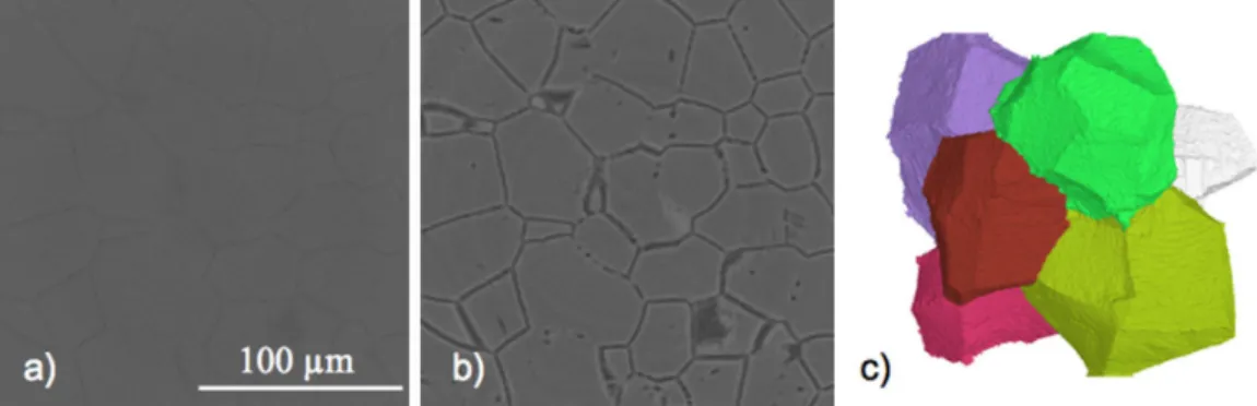
The use of polarized light can reveal the polycrystalline nature of the spec-imen as well. Here a polarizer is positioned in the light path, and because of the interaction between this polarized light and a birefringent material, grains can (mostly) be uniquely identified as shown in Fig. 1.1 (left). Using etch-ing techniques,grain boundaries can be specifically visualized through optical microscopy. They are more severely attacked by the etchant. This results in image contrasts because of the topographic differences, which will reflect the light differently. [Couling and Pearsall, 1957, Larson and Picklesimer, 1966] have demonstrated the possibility to determine the orientation of the c-axis in hexagonal crystal structures.
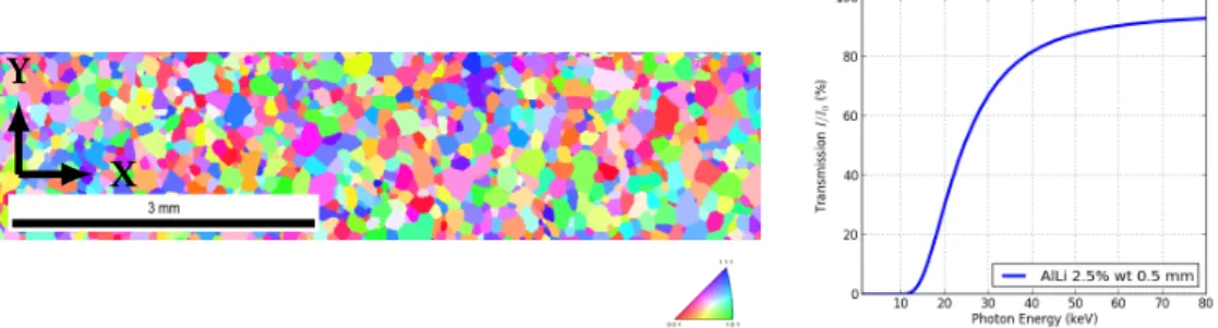
Figure 1.1 – Grain microstructure of a AlLi 2.5wt recrystallized alloy revealed by polarized light microscopy (left) and reconstruction of 4380 grains in a 1115 × 516 × 300 µm3 big volume of β-Ti alloy built from a stack of 200 serial sections
(1.5 µm spacing) by [Rowenhorst et al., 2010] (right).
A three-dimensional (3D) extension of the surface characterization is avail-able through serial sectioning. By repeating observation and the surface prepa-ration procedure, it is possible to reconstruct a 3D map of the microstructure. In a study by [Rowenhorst et al., 2010], 201 raw images were taken in a four weeks time frame. The final reconstruction of the volume, shown in Fig. 1.1 (right), grains have been segmented using dedicated image analysis routines ex-ploiting the etching contrast at the grain boundaries. This is obviously a
time-1Super resolution microscopy techniques are now available. A review of these techniques can
consuming method, and cannot be extensively used in the present from, but ef-forts have been made to completely automate the serial sectioning process. In [Spowart et al., 2003, Spowart and Mullens, 2008], the team at the USAF labora-tory demonstrates how with a specifically designed robot, it is possible to sig-nificantly increase the slice rate, up to 20 slices per hour. This automated pro-cess reduce significantly the difficulty of the image registration using a LVDT [Alkemper and Voorhees, 2001].
Optical microscopy, as well as other surface characterization techniques do not allow for time resolved 3D studies (4D studies), because of the destructive nature of the serial sectioning process.
1.2
Electron microscopy
Electron microscopes use a beam of electrons to illuminate the sample and a detector to measure the quantity of re-emitted electrons from this point. The first electron microscope was built in 1932 by [Knoll and Ruska, 1932] achieving a × 400 magnification, soon followed by the first supermicroscope (overcoming the resolution limit of the visible light) in [Ruska, 1934] with a × 12000 magnification (see Fig. 1.2 (left)).
Nowadays, electron microscopes have become a basic and widely used tool in most research laboratories for material characterization, and can mainly be categorized in two categories: Scanning Electron Microscopes (SEM) and Trans-mission electron microscopes. In TEMs, an electron beam that went through the sample is magnified, to get a picture of the structure in the sample. In SEMs, elec-trons reflected from the surface by a focused beam are detected, while a rectan-gular grid of the sample is scanned2. Users can switch between different modes,
that depend on what type of electrons (Auger, secondary, backscattered, etc.) are used to generate the image (see Fig. 1.2 (right)). 10 times more SEMs are available compared to TEMs..
The next two sections will deal with Transmission Electron Microscopy (TEM) and with Electron BackScatter Diffraction (EBSD), two techniques capable of re-vealing the crystalline structure of the materials and its defects. Secondary Elec-trons (SE) and BackScattered ElecElec-trons (BSE) modes are capable to reveal most of the grain boundaries, with a sample properly prepared3, but cannot give
quan-titative essential information about the crystal such as its orientation, and will not be discussed here.
2A comparable mode exists for TEM, where the transmitted electron from a focused beam are
detected, called Scanning Transmission Electron Microscope (STEM).
3A sample prepared by chemical or electro chemical etching will exhibit facets. As the etching
Figure 1.2 – One of the first image by an electron supermicroscope, a cotton thread magnified approximately 800× from [Ruska, 1934] (left), and the diagram of the interaction between electrons and matter (courtesy of Claudionico, com-mons wiki).
1.2.1
Transmission electron microscopy
TEM, for Transmission Electron Microscopy, uses a transmitted beam of electrons through a very thin (typically ≃ 100 nm) specimen, to generate an image. The electrons emitted by an emission gun interact strongly with the matter, and the analysis of the images thus requires an appropriate theoretical background to be properly analyzed. Since the forward-thinking speech of R. Feynman in 1959 There is Plenty of Room at the Bottom, where he stated The electron microscope is not quite good enough, with the greatest care and effort, it can only resolve about 10 angstroms ... Is there no way to make the electron microscope more powerful?, progress in the optics have permitted to reach resolutions up to 50 pm have been reached [Erni et al., 2009, Kabius et al., 2009, Miao et al., 2016]. Thanks to TEM and its variants (in particular the high-resolution transmission electron mi-croscopy (HREM) and the scanning electron transmission mimi-croscopy (STEM), huge advances have been made to the understanding of the behavior of materials at the nanoscale. The first ever direct image of a dislocation has been published by [Hirsch et al., 1956], and a remarkable review of the historical background leading to these breakthrough is available in [Hirsch, 1986].
Time resolve studies have been made with TEM, since the beginning of the development of the technique. Specifically designed stages, discussed in [Butler, 1979], capable of straining, heating, and cooling the observed sam-ples have been designed. It allowed scientists to develop in-situ experi-ments, and observe the formation [Thomas and Whelan, 1961] and the dilution [Laird and Aaronson, 1966] of precipitates in an AlCu alloy, phase
transforma-tions in [Hull, 1962], radiation damage in [Eyre, 1962], or recrystallization in [Roberts and Lehtinen, 1972]. Essential observations for the understanding of the plastic deformation process have been allowed by the development of me-chanical in-situ testing in TEM. The first movement of dislocations have been observed in [Hirsch et al., 1956] due to the beam heating of the sample. Early stages of plasticity have been studies by [Fujita, 1969] as well as fatigue in [Suga and Imura, 1976]. In-situ testing while taking images at a micrometer or nanometer scale is a difficult process. For TEM, [Martin and Kubin, 1978] discuss about the optimal setup for in-situ experiments.
With the availability of high voltage sources, the work of [Fujita, 1967] and colleagues have shown that the thickness of the sample is an important factor in the deformation behavior of the sample. Indeed, the main drawback of electron microscopes is to only allow observations in a very limited volume. Using sub-stantial volumes, representative of the overall behavior at the scale of interest is of prime importance to get a representative picture.
Three-dimensional extensions of TEM (3D-TEM) have been first available for biological samples in the late 90ś, and rely on the same principles as those used in X-ray tomography. 2D projections are recorded with small increments of the angular position, over a wide angular range. If a specific diffraction condition is maintained, and with the adequate reconstruction procedure (realignment, etc. [Frank et al., 1996]), [Barnard et al., 2006] have demonstrated that one can pro-duce a 3D map of crystal defects, like dislocations. Classic tomography recon-structions are also available from projections in imaging modes. Reconrecon-structions of small objects such as nanometric Pd particles or a Silica bead topped with a nickel nanocrystal are shown in [Ersen et al., 2007].
Orientation imaging is also available in TEMs. In diffraction mode, it is possible to record diffraction patterns, from different tilts of the sample, and to index the Laue patterns to reconstruct the local crystallographic orienta-tion. An EBSD like approach, called Automated Crystal Orientation and phase mapping in TEM (ACOM-TEM), can be adopted, where a nanofocused beam scans the sample and diffraction patterns are acquired rather than Kikuchi lines [Rauch and Véron, 2014]. Phase mapping is possible as well, and spatial reso-lutions down to ∼ 1 nm can be reached. The angular resolution is around 1° limited by the angular step size used to cover the orientation space, and ACOM-TEM is only relevant if the grain size is bigger than the thickness of the foil. The 3D extension of ACOM-TEM is presented in [Eggeman et al., 2015], where pat-terns are recorded pixel-by-pixel and tilt-by-tilt. The possibility to generate 3D orientation maps from TEM (without scanning the sample) in diffraction mode has been demonstrated in [Liu et al., 2011]. The authors have used simulated data and algorithms inherited from 3D X-ray diffraction (detailled further in this section) to prove that TEM diffraction patterns are relevant for 3D orientation
mapping without using a focused beam.
Finally, with the possibility to generate ultra short pulses of electrons, 4D studies have been released for electron microscopy. A 4D movie of the motion of a complex Carbone nanotube has been published in [Kwon and Zewail, 2010]. Here, the time scale (the pico second) used, is totally appropriate to observe the deformation behavior of materials and individual dislocation moving through the crystal lattice, and there is no doubt that in the near future formation of dislocations structure will be observed at the atomic scale in 3D.
1.2.2
Electron backscattered diffraction
The first EBSD patterns have been analyzed by [Coates, 1967], and the tech-nique is now routinely used in materials science facilities. It provides fully auto-mated [Wright and Adams, 1992, Kunze et al., 1993]. The technique is (typically) implemented in a conventionnal SEM, where diffraction patterns (Kikuchi pat-terns [Nishikawa and Kikuchi, 1928, Kikuchi, 1928]) originating from backscat-tered electrons, are collected on a dedicated high speed detector system consist-ing in a phosphor screen and a CCD camera. To maximize the back-scattered electrons signal, the sample is usually tilted at 70°. From the knowledge of the geometry and the crystalline phases existing in the sample, it is possible to gen-erate a precise map of local crystallographic orientation and phase. EBSD is in-trinsically a surface scanning technique, and the depth of the measurement, even though depending on the acceleration voltage and the atomic number of the ma-terial, is approximately 100 nm (but there is no general consensus and research is still conducted in this field [Wisniewski and Rüssel, 2015]).
The ultimate achievable spatial resolution of EBSD is 20 nm, and its angular resolution approximately 0.5°. High resolution modes have been developed [Wilkinson et al., 2006], and angular resolutions down to 0.004° have been reported, allowing the calculation of the GNDs density tensor in [Maurice and Fortunier, 2008, Ruggles and Fullwood, 2013] and elastic strains down a precision of 10−4 in [Wilkinson et al., 2006].
In-situ experiments for EBSD have been developed, to provide 2D-time re-solved studies. Specific tension rigs has been developed to fit EBSD require-ments (and more generally electron microscopy requirerequire-ments like vacuum and space constraints) like in [Chiron et al., 1997]. In [Bao et al., 2010], the authors present a study of the lattice rotation and the twinning of a Ti alloy, through several interrupted in-situ EBSD scans. In [Wright et al., 2016], the evolution of intragranular and overall lattice rotation is presented, as well as the variation of the local misorientation at grain boundaries due neighboring grains. As grains can be individually identified by EBSD, the recrystallization process can be mon-itored, like in [Zhu et al., 2005]. EBSD scans can be coupled to other techniques
to provide multi-channel data sets ("correlative microscopy"). As an example, EBSD coupled with digital image correlation of BSE images provides microex-tensometry [Doumalin and Bornert, 2000].
In [Lewis et al., 2006], the authors present a 3D reconstruction of an austenitic stainless steel. EBSD maps were taken every 33 µm and the reconstructed volume was 250 µm × 250 µm × 160 µm, comprising 138 layers and served as an input for an image-based finite element model to simulate the mesoscale mechanical response of the real microstructure [Lewis and Geltmacher, 2006]. The alignment of the layers was made using Vickers indent marks. This process can now be automated, using robots, as mentioned earlier. The more recent development of dual beams instruments
Figure 1.3 – Schematic of the principle of the tri-beam (left), and picture of the chamber of the microscope (middle). Reconstruction of a polycrystalline Nickel sample. From [Echlin et al., 2012].
(FIB4/SEM) extend the capability of a classical SEM instrument from 2D to 3D
analysis. Thin layers (down to 50 nm) of the sample can be removed by the ac-tion of the FIB on the sample surface, and at each step, a comprehensive anal-ysis taking advantage of the multimodal capabilities of the SEM (SE and BSE imaging, phase, orientation and composition analysis). The typical material re-moval rate by Ga ions drastically limits the volume of material which can be observed (100 µm × 100 µm × 20 µm). Plasma-FIB may be a way forward soon [Burnett et al., 2016], enabling the imaging of larger volumes. More recently, the team of Pr. Tresa Pollock at UCSB has developed a tri-beam microscope, adding a pulsed femto second laser to the previously presented system (Fig. 1.3) [Echlin et al., 2011, Echlin et al., 2012]. This femtolaser focused into a 1 µm spot provide micromachining capabilities by sequentially ablating the surface (com-pared to FIB micromachining, the material removal rate is several orders of mag-nitude higher, which allow to image a much larger volume of material).
1.3
3D X-ray microstructure characterization
techniques
While the serial sectioning techniques rely on sequentially removing thin lay-ers of the samples to provide 3D data, the techniques presented in this section make use of the penetration power of X-rays through matter to provide non-destructive orientation or defect maps.
1.3.1
Laue micro diffraction
Laue diffraction is the oldest X-ray analysis technique. A polychromatic beam illuminates a crystalline sample giving rise to a diffraction pattern onto a detec-tor (an X-ray sensitive photographic plates in the old times), see Fig. 1.4. Here the spatial resolution is linked to the focalization of the X-ray beam. Nowa-days, with the great improvement of X-ray optics, polychromatic beams (typi-cally within the range of 5 and 35 keV5), beams can be focused down to about
a 7 nm spot size [Mimura et al., 2010], although in DXWM 100 nm are rather used. With the acquisition of several Laue patterns, through an indexing and position refinement procedure, it is possible to retrieve not only crystal orien-tation, but the deviatoric elastic strain tensor. The accuracy of these analysis is respectively 0.1° and 10−4. For the hydrostatic component of the elastic tensor,
the energy of at least one reflection must be done, in addition to the white beam data [Robach et al., 2011]. For that purpose, the microlaue diffraction beamlines are equipped with specific optics which allow to switch between polychromatic and monochromatic modes. A direct application of the technique was the high-resolution grain mapping shown in [Tamura et al., 2002]. In situ testing of FIB milled single crystal micro pillars has been made in [Maaß et al., 2007]. Which confirmed the importance of preexisting strain gradients in the slip system acti-vation.
A depth resolved variant of the technique allowing the analysis of bulk sam-ples has been developed in [Larson et al., 2002, Robach et al., 2014], called Differ-ential aperture X-ray microscopy (DAXM). It consists of the acquisition of diffrac-tion patterns while an absorbing thin wire (typically made of tungsten) moves close to the sample surface. By analyzing the different images at each position of the beam, it is possible to perform a triangulation and therefore to know the origin of each diffraction spot. For optimal spatial and temporal resolutions, the wire should be placed close to the surface of the sample. This in turn complicates the extension to 4D studies, due to severe space constraints limiting the possi-bility to include a mechanical test rig into the setup. A reconstructed grain map
Figure 1.4 – A Laue diffraction pattern (left, courtesy of the ESRF), and a recon-structed microstructure of a CeO2film on a Ni substrate from [Ice et al., 2005].
is shown in Fig. 1.4 (right).
1.3.2
X-ray microtomography
From the pioneering work of [Cormack and Koehler, 1976, Hounsfield, 1980] and the first invention of a computed tomography (CT) scan, first applied to medical diagnosis, computed tomography has quickly grown up, thanks to the improve-ment of both sources and detectors, it is nowadays a widely used tool for mate-rials science, enabling non-destructive, three-dimensional analysis of bulk sam-ples. from the nanometer6to the millimeter range. Every synchrotron radiation
facility now accept CT experiments, and plenty of manufacturers provide CT lab solutions, overcoming the intrinsically limited access to synchrotron beamlines. Here, we will focus on applications of synchrotron radiation CT.
Computed tomography, or more commonly named X-ray computed micro-tomography in the field of material science, is based on the acquisition of a set of 2D projections on a high resolution detector. The sample is fixed on a turntable and several images are taken for different angular positions. Al-though many different variants of reconstruction algorithms exist, 3D recon-structions are typically obtained via filtered back projection developed origi-nally by [Feldkamp et al., 1984]. Synchrotron X-ray beams are partially coherent, which makes the detector image a combination of absorption and phase contrast, the later being dependent on the sample detector distance. Due to this, there are mainly three different acquisition modes available for material characterization [Salvo et al., 2003]. In the absorption mode, contrasts arise from the differences of density and atomic number of the material. In this case the detector is placed close to the sample (hence no phase contrast), this mode is not suitable if the
difference of density between the components is too small. When the detector is placed further away (in the edge detection regime), contrasts in the projections as well as in the reconstructed volumes arise from the interferences, revealed by the refraction of the electromagnetic wave in the material. A phase retrieval algorithm for the reconstruction in the edge detection regime is described in [Paganin et al., 2002], but degrades the spatial resolution. In the later, the real part δ of the refractive index is reconstructed7. This technique is called Phase
Contrast Tomography (PCT). By taking images at several propagation distances, and applying a special phase retrieval algorithm (inspired by the high-resolution electron microscopy) presented in [Cloetens et al., 1999] called holotomography, a quantitative analysis of the material density is possible. This latter mode is especially suited when previous modes fail to provide contrast. The difference between the different modes is shown in Fig. 1.5.
Figure 1.5 – Comparison of slices reconstructed by (a) absorption tomogra-phy, (b) phase contrast tomogratomogra-phy, (c) holotomography. The sample was an austenitic/ferritic steel, from [Ludwig, 2010]
As monophasic polycrystalline materials do not exhibit contrasts between grains in term of electronic densities, the previous techniques are not suit-able to provide insight into the grain structure. To reveal the grain bound-aries, it is possible to decorate the grain boundaries with a liquid phase as demonstrated in [Nicholas and Old, 1979]. Liquid Gallium has been used in [Ludwig and Bellet, 2000] to reveal the grain microstructure of an Aluminum alloy, as well as interactions between a fatigue crack and grain boundaries in [Ludwig et al., 2003]. When infiltrated, the Gallium penetrates and diffuses along the grain boundaries which in turn can be reconstructed by means of absorption contrast. One important drawback of this method is that Gallium completely changes the mechanical properties, and makes metals like Al and Zn alloys
tle8. It is therefore not possible to perform in-situ studies with the Gallium
em-brittlement method. Another solution is to use the segregation of alloying el-ements at grain boundaries [Ludwig, 2010]. In some cases, GBs are preferred sites for phase transformations, and the contrast of layer-like GB precipitates can be retrieved by PCT as shown in [Dey et al., 2007], or in [Dake et al., 2016] where the GBs show a higher concentration of Cu and are observable by PCT. These methods will only work in a limited number of material systems and only provide the 3D grain morphologies without access to their orientation. Crystal-lographic orientations and defects play a major role in the mechanical behavior of materials, and for that purpose, there is a need for combined diffraction and imaging techniques, as exposed in [Ludwig, 2010]. This will be covered in the next subsections.
Figure 1.6 – Tomographic reconstruction in the absorption regime (a), and the phase contrast regime (b) of sample made from a metastable β-Ti alloy. Volume rendering of the grains from the segmentation (c). The alloying layer-like pre-cipitation of α-Ti at the grain boundaries is visible in the phase contrast regime. From [Ludwig et al., 2009b].
1.3.3
X-ray diffraction topography
Overview of X-ray topography
Images of the surface or the interior of a single crystal formed by X-ray Bragg reflected from its lattice planes provide information about lattice misorientations and defects in a unique way [Lang, 1993]. X-ray diffraction topography has been widely used since the first topographic experiment has been published by [Berg, 1931, Barrett, 1931], which have respectively observed plastic defor-mation on rock salt and elastic strains in quartz crystals. The capability of
the different topographic techniques to reveal defects in crystalline structures has been of prime interest, especially when crystal quality is crucial like for the semi-conductor industry. The technique consists in recording on a 2D de-tector, the Bragg (or Laue9) reflection of a crystal (single crystal or a grain
embedded in a polycrystal). Different imaging modes can be used: polychro-matic [Ramachandran, 1944, Guinier and Tennevin, 1949], or monochropolychro-matic as Berg in 1931, and with both X-rays produced by conventional X-ray tubes or synchrotron radiation [Tuomi et al., 1974]. From the analysis of the inten-sity variations in the reflections (see below for more details on the physi-cal processes involved), it is possible to determine the spatial location of de-fects like dislocations. For instance, studies have been carried out in neu-tron irradiated [Young Jr et al., 1965] and deformed [Young Jr and Sherrill, 1972] Copper samples. Many different setups exist, and have been reviewed in [Black and Long, 2004].
In synchrotron X-ray topography, both transmission and (back)reflection ge-ometries are used, and defects like precipitates, stacking faults, voids and dislo-cations have been observed. The main assets of synchrotron topography are the high flux allowing low exposure times, and the long source to sample distance increasing drastically the spatial resolution. The ultimate geometric resolution r is given in [Tuomi, 2002] as:
r = s
Lw (1.1)
with s the sample to detector distance, L the source to sample distance, and w the size of the source. For the monochromatic case, a previous indexing of the crystal thanks to a Laue pattern is required, or the crystal can be aligned to fulfill the Bragg condition by the method exposed in [Ludwig et al., 2007a] consisting in the determination of the diffracted vector by taking images of a reflection at different sample to detector distances.
Contrasts in the topographs
Different mechanisms can give rise to contrasts arising within the 2D to-pographs, an example of some of them is given in Fig. 1.7 (right). First extinction contrast in high quality (like recrystallized) crystals might occur due to dynami-cal diffraction. When the grain, or the sub-grain, size is comparable to or bigger than the Pendelloesung period, dynamical diffraction can occur and contrasts arise in the topographs. For example, in an aluminum crystal illuminated with
9It depends if the setup uses reflection geometry (Bragg case) or transmission geometry (Laue
a 40 keV radiation, the Pendellöesung period will be around 70 µm for the (111) reflection in the Laue case.
Figure 1.7 – Schematic of the Bragg diffraction (left, courtesy of wikimedia com-mons) and identification of the contrasts in an X-ray topography of a diamond single crystal (right, courtesy of the ESRF).
In deformed crystals, orientation contrasts may arise due to local modifica-tions of the Bragg condition. In polycrystals, a strong heterogeneity of elastic and plastic strains arise under loading. Elastic strains lead to local variations of the interplanar distance and angles, which in turn can result in a modification of the Bragg condition, see Fig. 1.7 (left). Plastic strains can lead to even higher lattice rotations. To ensure the geometrical compatibility of the material sub-volumes, geometrically necessary dislocations (GNDs) densities arise, as well as lattice curvatures [Ashby, 1971]. Locally, the crystal is not exactly oriented as the rest of the grain, and this leads again to a local modification of the Bragg condition.
A variety of other effects can lead to contrasts in topographs. Dislocations for example generate a contrast under certain geometrical conditions (g .b = 0) between the Burgers vector b of the dislocation and the scattering vector g . Generally speaking, two types of contrasts can be identified in topographs: ori-entation contrasts explained by the Bragg law (local variations of the directions of the diffracted beams), and defect contrasts, explained by means of the kinemat-ical and the dynamkinemat-ical diffraction theory [Zachariasen, 2004]. A comprehensive review of the contrast mechanisms in topographs can be found in [Tanner, 1976].
Variants of X-ray diffraction topography
Two variants of X-ray diffraction topography shall be presented in more details. They both consist in imaging the defect structure of crystalline materials. They are based on the classical Bragg imaging (monochromatic diffraction topogra-phy) presented previously, and can be extended to provide 3D maps of the de-fects.
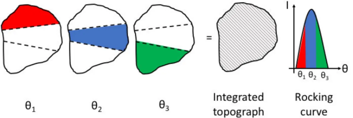
Rocking curve imaging (RCI) is based on the simple idea that if a crystal is illuminated by a wide (2D) monochromatic beam and fulfills the Bragg condi-tion, topographs can be recorded for different tilt angles of the rocking curve (RC). It is then possible to provide a space resolved map of rocking curves. This is a combination of X-ray topography and X-ray diffractometry, and the de-velopment of this technique has been possible thanks to the improvement of synchrotron sources and imaging detectors, decreasing drastically the exposure time for each image. It is possible with such data to analyze local variations of the lattice parameters by taking images for different reflections, and measur-ing the deviation of the peak positions of the RC. The full width at half max-imum (FWHM) of these RCs is linked to the intragranular orientation spread of the crystal, giving information about the GND density. RCI imaging pro-vides a map of these quantities. Studies of the quality of crystals have been published this way, in [Hoszowska et al., 2001] for diamond single crystals, or [Lübbert et al., 2000, Mikulík et al., 2003] for GaAs wafers. A 3D variant exists for this technique, called three-dimensional rocking curve imaging (3D-RCI), published in [Kluender et al., 2011, Kluender, 2011]. Here a line beam delimited by a slit, will illuminate the sample. By applying the previously presented method (diffraction topography) for different slices, it is possible to reconstruct a 3D map of the rocking curves. In this study, with another variant called pinhole topog-raphy, the authors add the possibility to scan the lateral deflection of the beam out of the diffracting plane. The method has been successfully applied to an ice tri-crystal, and an in-situ study has shown in [Philip et al., 2013] the formation of a subgrain boundary after applying a compressive load to the ice sample (see Fig. 1.8).
Another variant of topography is the Dark Field X-ray Microscopy (DFXM). This time, the principle is to magnify the diffracted beam by placing be-tween the sample and the detector a set of compound refractive lenses (CRL, [Snigirev et al., 1996]) (the latter are more suitable for energies used to scan sam-ples of interest in the field of engineering, above 15 keV, than Fresnel Zone plates). The image on the detector is a magnified projection of the grain in the di-rect space. The grain can either be illuminated by a line beam (1D) or a box beam (2D). The sample is mounted on a 4-circles diffractometer, and is aligned in a way that a grain fulfills the Bragg condition. The imaging lenses are mounted on a
Figure 1.8 – 3D rendering of the dislocation structures within an ice tri-crystal, imaged by 3D-RCI, from [Philip et al., 2013].
multi axis rotation and translation stage to ensure a proper alignment. The small numerical aperture (less than 4 × 10⁻⁴) of the CRLs allows to filter diffracted
beams from locally misoriented subvolumes of grain. The use of CRLs allows spatial resolutions down to 100 nm (20 nm are expected in the future with the use of Multi Laue lenses [Simons et al., 2016]) and angular resolutions better than 1 mrad. Then, by scanning the different tilts of the sample goniometer, a map of the local orientation within the grain can be produced. A schematic of the setup is presented in Fig. 1.9 (left).
Figure 1.9 – Principle of the DFXM (left), and 3D rendering of local orientation in a grain (middle) and its subgrains (right). From [Simons et al., 2015a].
The recovery of aluminum has been studied with this technique in [Simons et al., 2015a, Ahl et al., 2015], see Fig. 1.9 (right). The three-dimensional
characterization has been conducted by scanning different slices of the grain and merging them. The imaging of individual ferro-electric domains was also studied [Simons,not published], as well as individual embedded dislocations in a diamond single crystal [Jakobsen et al., 2016]. This method is non-destructive, and allows for in-situ studies, both during thermal and mechanical loading. Alongside the in-situ device presented in Chap. 2, a tiny compressive rig (not presented here) suited for in-situ DFXM studies has been developed in the frame of the present work.
1.3.4
Three-dimensional X-ray diffraction
The term of "Three-dimensional X-ray diffraction" (3DXRD) refers to a variety of techniques based on the monochromatic rotation method, starting from the pioneering work of [Poulsen et al., 2001, Lauridsen et al., 2001a, Poulsen, 2004a]. Although different variants exist, the basic principle remains the same: a poly-crystalline sample is illuminated by a monochromatic beam (most of the 3DXRD setups use the illumination by a laterally extended 1D line beam, and repeat acquisitions for several slices of the sample.). At each angular position of the ω-rotation stage, a subset of grains fulfilling the Bragg condition give rise to diffraction spots on a far field 2D detector. In the near-field variant, the acqui-sition may have to be repeated at several distances to measure the diffraction vector of a given spot (or the use of a 3D detector -structured scintillator- as in [Olsen et al., 2009], which allows ray tracing) see Fig. 1.10. By indexing the spots, it is possible to know the orientation, and the position of the center of mass of the grains of the illuminated sample volume. The technique has continuously evolved during the past 15 years, in term of setups, reconstruction algorithms, and its ability to measure additional physical quantities such as strain. It will be developed in the next paragraphs.
In [Lauridsen et al., 2001b] the authors published the first monochromatic beam indexing algorithm applicable to polycrystals called GRAINDEX. It is based on the detection of spots recorded at two or three different detector distances (see Fig. 1.10) matching criteria in terms of size and intensity. Due to its mosaicity, a grain can give rise to spots over a certain ω range. These detected spots at differ-ent distances are grouped into reflections, and a ray tracing algorithm iddiffer-entifies the possible diffraction vectors associated. To index the different grains of the sample, the algorithm groups them into grains, the intersection of the diffrac-tion vectors being at the center of mass of a grain. The orientadiffrac-tion of a grain is calculated by scanning the orientation space and choosing the best fit given the diffraction vectors associated to the given grain.
With these very first experiments, it was possible to extract a grain map from the diffraction data, giving for each grain the average orientation of the crystal
Figure 1.10 – Sketch of the principle of a 3DXRD experiment, from [Lauridsen et al., 2001b, Poulsen, 2004b].
and the average strain state. To reconstruct the shape of the grains, back projec-tions of the diffraction spots close to the pole were used in [Poulsen et al., 2001]. This idea was extended to algebraic reconstruction procedures to take into ac-count more spots for each grain, and increase the accuracy of this reconstruc-tion in [Fu et al., 2003, Fu et al., 2006]. New computareconstruc-tional capabilities allow the reconstruction of the orientation to be associated with forward modeling rithm. By simulating the diffraction spots for all possible orientations, these algo-rithms simulate a diffraction pattern, compare it with the experimental data, and iterate to minimize the differences. Several of these algorithms have been imple-mented, like GRAINSWEEPER (Søren Schmidt, DTU) or [Li and Suter, 2013a] at LLNL and CMU. An example from the work of [Li, 2011] is shown in Fig. 1.11. A near field variant of the 3DXRD technique, called diffraction contrast tomogra-phy (DCT) which has been used in this work, is presented in more details in Sec. 2.3.1.
One direct application of 3DXRD was the study of recrystallization. In [Schmidt et al., 2004] it was shown how it is possible to watch the morphol-ogy of a single grain growing during recrystallization (see Fig. 1.12), and how these observations are in contradiction with the established knowledge. [Lauridsen et al., 2006] studied the kinetic of the recrystallization of individual grains, and [Hefferan et al., 2012] used the new possibilities provided forward modeling approach to identify the growth of new grains related to intragran-ular microstructures. The plastic deformation of polycrystalline samples has
Figure 1.11 – Orientation maps of a high purity Ni sample, reconstructed by a forward modelling approach, for three different applied loads. From [Li, 2011]. been studied in [Margulies et al., 2001] who compared the grain rotations in-duced by the deformation with the Taylor model. By studying the intensity distribution in the reciprocal space, [Jakobsen et al., 2008, Pantleon et al., 2009] were able to identify the formation of dislocation structures, and the forma-tion of subgrains. Fatigue of engineering materials has also been studied. In [Obstalecki et al., 2014], the authors show the effect of cyclic deformation on the spread over η and ω of the spots. Strain and stress fields within a polycrystal have been extensively studied using this method, as in [Oddershede et al., 2012, Sedmák et al., 2016].
Figure 1.12 – Grain growth imaged by 3DXRD, from [Schmidt et al., 2004]. Most of the previous mentioned studies are time-lapse studies (interrupted in-situ). The main asset of these techniques is the use of the penetration power of X-rays, allowing non-destructive analysis. It is then possible to observe the evolution of physical parameters (crystal orientation, grain size and shape, strain, etc.). Space constraint as well as required accuracy make the use of in-situ me-chanical stress rig difficult. In the US, a joint effort of CHESS, APS, and the Air Force National Laboratory lead to the design of a rotational and axial motion
system [Blank et al., 2016]. It allows the sample to rotate under load within the required accuracy and take advantage of the robust load frame from MTS. In Chap. 2, a new design adapted to the DCT geometry and allowing for 4D studies of polycrystalline specimen will be presented.
Materials and methods
Ce chapitre décrit le matériau et les techniques expérimentales utilisées dans le cadre de ce travail.
Premièrement, une revue historique, et une revue du comportement mécanique des alliages d’Aluminium-Lithium est faite. Les caractéristiques du matériau choisit pour ce travail, un alliage binaire d’Aluminium contenant 2,5% de Lithium sont exposées.
Dans une seconde partie, les deux techniques expérimentales sur lesquelles reposent ce travail sont détaillées : la tomographie par contraste de diffraction et la topo-tomographie. La tomographie par contraste de diffraction permet de connaitre la position, la forme, et l’orientation des grains qui composent un polycristal. Avec la topotomographie, l’attention est portée sur un grain en particulier. La technique permet de reconstruire en trois dimensions les défauts cristallins qui perturbent la diffraction du cristal.
Enfin, afin de disposer d’un moyen d’essai mécanique adaptée aux techniques précédemment exposées, une machine de traction miniature appelée Nanox a été développée. L’article, publié dans Journal of synchrotron radiation, traite de ces développements est inclu est attache dans la troisième partie de ce chapitre.
2.1
Introduction
This chapter provides the necessary details on the material and the methods used throughout this work. First, a short review on Aluminum-Lithium (AlLi) alloys is given, with a focus on the metallurgy and the deformation behavior of binary AlLi alloys. The second part of this chapter shows how it is possible to study microstructural evolutions of polycrystalline materials with two dif-ferent three-dimensional diffraction techniques namely diffraction contrast to-mography and topototo-mography. At the end, the design of a specific tensile rig allowing for 4D diffraction studies is detailed. This last part was published in [Gueninchault et al., 2016].
2.2
Material: Review of the properties of binary
AlLi alloys
2.2.1
Developments of AlLi alloys
Structural weight reduction is a very efficient way to improve aircraft perfor-mance [Joshi, 2005]. To this end, AlLi alloys with their low density and their good mechanical properties, are of high interest for the aeronautical industry. Most of the developments for these alloys were led by the need of greener and safer planes, as the traffic has increased from 106 million in 1960 to more than 6 billion passengers-kilometers in 2016 (ICAO statistics). Extensive reviews of the devel-opment of these alloys can be found in the work of [Proton, 2012, Cerutti, 2014, Delacroix, 2011] as well as in [Lavernia and Grant, 1987] for the microstructural and the mechanical behavior of AlLi alloys.
AlLi alloys have been widely used in aircraft structures since the 1920s [Prasad et al., 2013], and mainly four phases in the development of the AlLi al-loys can be distinguished since the fifties:
• The first phase, beginning in the 1950s, with the development of the AA20201alloy from ALCOA and the VAD20 from the USSR industry. They
were developed mainly for fighter aircraft applications (the F20 tigershark program of the US department of defense for the AA2020 alloy, later aban-doned for the famous F16). This first generation of AlLi alloys was with-drawn because of their low toughness and low ductility.
• The second generation of alloys began with the oil shock of 1970-1980 [Cerutti, 2014] and the design of supersonic aircrafts like le Concorde
![Figure 1.2 – One of the first image by an electron supermicroscope, a cotton thread magnified approximately 800× from [Ruska, 1934] (left), and the diagram of the interaction between electrons and matter (courtesy of Claudionico, com-mons wiki).](https://thumb-eu.123doks.com/thumbv2/123doknet/2898648.74513/24.892.125.705.177.438/electron-supermicroscope-magnified-approximately-interaction-electrons-courtesy-claudionico.webp)
![Figure 1.8 – 3D rendering of the dislocation structures within an ice tri-crystal, imaged by 3D-RCI, from [Philip et al., 2013].](https://thumb-eu.123doks.com/thumbv2/123doknet/2898648.74513/35.892.182.772.184.457/figure-rendering-dislocation-structures-crystal-imaged-rci-philip.webp)
![Figure 2.2 – Schematic of the softening mechanism (left) and micrograph of plas- plas-tic strain localization in AlLi alloy from [Sanders and Starke, 1982].](https://thumb-eu.123doks.com/thumbv2/123doknet/2898648.74513/44.892.139.605.429.623/figure-schematic-softening-mechanism-micrograph-localization-sanders-starke.webp)