Open Archive TOULOUSE Archive Ouverte (OATAO)
OATAO is an open access repository that collects the work of Toulouse researchers and
makes it freely available over the web where possible.
This is an author-deposited version published in :
http://oatao.univ-toulouse.fr/
Eprints ID : 19295
To link to this article : DOI:
10.1016/j.mtphys.2017.12.002
URL :
http://dx.doi.org/10.1016/j.mtphys.2017.12.002
To cite this version :
Kumar, Sunil and Maury, Francis and
Bahlawane, Naoufal Light modulation in phase change disordered
metamaterial - A smart cermet concept. (2017) Materials Today
Physics, vol. 3. pp. 41-47. ISSN 2542-5293
Any correspondence concerning this service should be sent to the repository
administrator:
[email protected]
Light modulation in phase change disordered metamaterial - A smart
cermet concept
Sunil Kumar
a, Francis Maury
b, Naoufal Bahlawane
a,*aLuxembourg Institute of Science and Technology (LIST), 5 avenue des Hauts-Fourneaux, L-4362 Esch-sur-Alzette, Luxembourg bCIRIMAT, ENSIACET-4 all!ee E. Monso, 31030 Toulouse, France
Keywords: Metamaterial Smart cermet Vanadium oxide MOCVD Emissivity control Solar selective coatings Semiconductor-metal transition
a b s t r a c t
Cermet coatings are popular solar selective absorbers as they allow capturing most of the solar energy while minimising radiative losses. Embedded metallic nanoparticles in dielectric matrices promote multiple internal reflection of light and provide an overall low emissivity. VO2in the metamaterial state
is regarded in this study as a responsive mixed phase comprising metallic rutile VO2 inclusions in
semiconducting monoclinic VO2phase mimicking cermet. The smart cermet responds to thermal stimuli
by modulating the size of the metallic inclusions and thereby enabling the manipulation of their interaction with light. The highly reliable and reproducible response of the smart cermet corroborates with the observed ramp reversal memory effect in VO2. We demonstrate a thermally controlled 85%
emissivity switch taking advantage of the narrow hysteresis and tuning abilities of the disordered metamaterial.
Introduction
Cermets are metal-dielectric composites in which metal parti-cles are embedded in dielectric matrices as displayed in Fig. 1. Cermet coatings are used as effective spectrally-selective absorbers due to their high solar absorbance and low thermal emittance[1,2]. The properties of the cermet strongly depend on the volume frac-tion of the metal inclusions in addifrac-tion to their chemical nature, size, shape and dispersion within the matrix[3]. Nevertheless, the properties of the cermet coatings are frozen upon synthesis as the parameters influencing the optical properties can no longer be altered. Therefore, the development of traditional cermet materials for light modulation sounds compromised.
One of the most popular and well-studied mechanisms for light modulation relies on materials with engineered structures to in-fluence the nature of light. These materials are known as meta-materials and the phenomenon of light modulation through engineered surface modifications is termed as optical topological transition [4,5]. Perfect solar absorbers based on metamaterials were demonstrated by fabricating specific shapes and
configurations of metallic structures on dielectric matrix. By vary-ing the size and configuration, the spectral window of the perfect absorption can be adjusted[6,7].
Relevant research was reported on emissivity control devices for their implementation in space applications. Programmable emis-sivity switching is crucial for spacecraft and satellite surfaces, but their implementation often includes tedious fabrication process comprising bulky and energy inefficient mechanisms[8e11]. Sig-nificant research has been done in the field of thermal management for spacecraft and satellites, due to varying exposure to sun illu-mination. Variable heat rejection surfaces are used to control the heat dissipation mechanisms. One of the earliest techniques of thermal management of spacecraft is by the use of mechanical or electric louvers, where actuating the louvers exposes or conceals a section of surface with a contrasting emissivity, thereby reflecting the IR radiation on demand. Electric louvers based on micro-electro-mechanical systems (MEMS) were introduced to further improve the same mechanism and miniaturise the package [9]. Here micro-sized windows open and close on demand to reject IR radiation. An advantage of MEMS based louvers over their bulk mechanical counterparts is the possibility to achieve partial IR rejection by actuating only a part of the micro-louvers[9]. Elec-trochromic devices that rely on chemical changes to vary the
*Corresponding author.
E-mail address:[email protected](N. Bahlawane).
emissivity of the surface are investigated as alternative solutions to change the optical properties of the radiating surface. An electri-cally triggered redox reaction on conductive polymers leads to a change of emissivity (DƐ). The absence of moving parts is advan-tageous in terms of production cost, reliability and integration[10]. Nevertheless, slow switching; high input power and the relatively low
D
Ɛ remain clear drawbacks. This strengthens the need of developing variable emissivity coatings that offer large amplitude of emissivity change, with negligible switching delay and low actuation power. The coatings should also virtually have no loss in performance over a longer time period and should resist environ-mental degradation. Therefore, inorganic metal oxide coatings with intrinsic phase transition behaviour are an appealing alternative. Ideally the phase transition occurs instantaneously between two strongly contrasting emissivity states without involving any chemical change.An ideal candidate for such application would be a coating material that switches reliably between distinct values of emis-sivity, and which is simple to fabricate and integrate, while consuming fraction of the power needed for existing technologies. Vanadium dioxide is a strongly correlated material featuring a semiconducting-to-metal transition (SMT) near room temperature. In contrast to the metallic phase, the low temperature semi-conducting phase features high infrared transmission and high thermal emissivity. The transition occurs with a narrow hysteresis, revealing a temperature range (64e68!C) where vanadium oxide
features the coexistence of the metallic and semiconducting pha-ses. This, so called disordered VO2metamaterial is analogous to a
cermet. Upon the increase of temperature, metallic inclusions nucleate and grow throughout the semiconducting phase[12]. In this article we introduce the concept of “smart cermet” material with tuneable optical properties based on disordered VO2
meta-material. The concept of tunability is addressed by temperature-enabled control of the size and density of metallic particles in the dielectric matrix which in turn vary the emissivity of the coating. The unique feature of VO2-based smart cermet is that, both
dielectric matrix and metallic particles are one and the same ma-terial at different phases. Therefore, a single layer of VO2can be
manipulated to feature (i) a fully dielectric state, (ii) a variable state with metallic inclusions embedded in the dielectric matrix, or (iii) a fully metallic state, by controlling the temperature at which it is operated. Such characteristics are not accessible with conventional cermet coatings. Thermally triggered emissivity modulation is emphasized in this study.
Methods
VO2 films were deposited on silicon substrates using direct
liquid injection MOCVD (MC200 from Annealsys), which is a stag-nation point-flow warm-walled reactor. Cyclohexane solution containing 5 " 10#3mol/l of vanadium (IV) oxy-tri-isopropoxide [VO(iOC3H7)3] is used as a precursor feedstock that was
maintained under nitrogen atmosphere at room temperature before its injection into the evaporation chamber. The precursor delivery was performed at a frequency of 2 Hz and a feeding rate of 1 g/min. The pressure and temperature of the evaporation chamber were maintained at 0.6 mbar and 200 !C during deposition
respectively. The substrate is maintained at 600!C during the 2 h of
deposition and the subsequent heat treatments.
One hour annealing was performed right after the deposition under oxygen partial pressure of 1 " 10#2mbar. The sample is then further subjected to annealing under vacuum acting as a reducing atmosphere for 4 h. The chamber is allowed to cool down to withdraw the sample. All depositions were carried out on 4-inch silicon wafers with an upper native oxide layer. Uniform and high quality VO2 films were observed throughout the wafers with
excellent homogeneity.
Film thickness was measured using an Alpha step d-500 pro-filometer from KLA-Tencor, whereas the Infrared image analysis was conducted using the FLIR X6580SC thermal camera operating in the spectral range of 1.5e5.1
mm. A CVD-grown CNT on silicon
was used as a reference black body for an accurate determination of temperature, which is necessary to assess the emissivity change of coated VO2. Precise temperature control was achieved through aLinkam TMS heating stage with programmable heating and cooling profiles. The stage is widely used for its accurate temperature control of heating/cooling rates with high ability to maintain a particular temperature for extended periods (>100 h) and has the ability to increase or decrease the temperature at the rate of up to 150!C/min with no measurable overshoot. The heating or cooling
pulses are programmed, and the set values are produced with di-vergences less than 0.01 !C. The inspection of the surface
morphology was performed by Scanning Electron Microscopy (SEM) at a working distance of 4 mm and an acceleration voltage of 5 kV. It is worth mentioning that the electron beam of the SEM induces the SMT of VO2from the semiconducting monoclinic phase
to the metallic rutile, which is beneficial for the charge dissipation. The identification of the crystalline phases was performed with X-ray diffraction (XRD: Bruker D8 and with CuKaas the X-ray source) and Raman scattering (InVia, Renishaw with a 532 nm laser). Results and discussion
The process used for the synthesis of VO2includes CVD
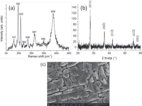
depo-sition and an oxidative sintering as a post-depodepo-sition heat treat-ment. Using this process the deposition rate was evaluated at ~10 nm/min. The prepared films are clearly identified as monoclinic VO2 at room temperature by Raman spectroscopy. Displayed
spectrum inFig. 2a features all characteristic Raman bands of the VO2monoclinic phase, which can be clearly distinguished from the
other phases of vanadium oxide[13]. The obtained films do not feature any Raman band above 68!C, which indicates the
occur-rence of a structural transition.
The room temperature X-ray diffractogram,Fig. 2b, of the ob-tained films confirms their identification as crystalline monoclinic VO2. The SEM surface inspection,Fig. 2c, reveals a dense structure
with large grains witnessing an efficient sintering of the film. Thermal camera was implemented in this study to investigate the VO2phase transition from semiconducting monoclinic to the
metallic rutile that occurs with thermal cycling. As the metallic phase features a low thermal emittance, the surface appears colder above the transition upon heating, a phenomenon that was termed as negative differential thermal emittance[14]. The VO2emissivity
versus temperature upon cycling between 60 and 70!C, Fig. 3,
features three distinct regions marked (a), (b) and (c). During heating stage the system undergoes an abrupt semiconductor to metal transition (SMT) at 67.5!C resulting in an emissivity drop Fig. 1. Schematic presentation of cermet coating.
from 0.8 to 0.1 within a
DT of 2
!C. The infrared images inFig. 3(i),(ii) and (iii) provide a visual representation of the material under-going SMT, by formation of metallic puddles in the semiconducting phase, which grow in number and coalesce, thus making the whole layer metallic. These metallic puddles reflect infra-red radiation and lower the overall emissivity[12e14].
In the cooling stage, emissivity features a transient peaking up to 0.94 at 63.5!C marked as (a) in Fig. 3. This peculiar peak of
emissivity is highly reproducible and is systematically observed for
all performed coatings. This kind of negative differential thermal emittance was previously reported by Kats et al.[14,15]where VO2
as a tuneable phase change material was shown to operate both as perfect emitter[14]and absorber[15]. The peak in the emissivity curve is attributed to the formation upon cooling of nanoscale metallic inclusions in an arrangement that maximizes light ab-sorption. At 63.5!C the density and size of the metallic inclusions
align in such a way that a near perfect thermal emittance is reached. The demonstrated,Fig. 3, change in emissivity from 0.8 to 0.1 (DƐ ¼0.7), or 0.94 to 0.1 (DƐ ¼ 0.84) using VO2coatings, is
unprecedented with conventional variable emissivity coatings used in space applications[16,17].
Perfectly reversible and reliable emissivity transition is recorded for VO2films during extended thermal cycling tests. Furthermore,
the transition characteristics were shown to be insensitive to the cycling rate. The stability of the metamaterial state is demonstrated in a previous work, where Raman mapping of the mixed phase region was reported over 100 h to obtain a spatial mapping of the metallic inclusions in the semiconducting matrix[13].
The metallic inclusions nucleate and grow upon heating, and shrink to disappear in the cooling stage. During a subsequent cycle, IR imaging reveals the nucleation of the metallic phase exactly at the same positions and confirms its systematic growth in an identical manner as the preceding heating cycle for consecutive cycles. This behaviour is in line with the ramp reversal memory effect in VO2 reported recently [18], where the nuclation of the
metallic puddle during the heating cycle occurs at the same spot over successive cycles. This behaviour is of paramount importance for a tuneable and reliable light modulation.
The polycrystalline nature of the films results in a random strain field distribution across the film. As the transition temperature of VO2is significantly influenced by the stress[19,20], crystallites do Fig. 2. Raman scattering (a), XRD (b) and the SEM (c) surface morphology of the VO2obtained via oxidative sintering. The (hkl) assignments correspond to the monoclinic VO2
reference pdf no. 44-0252, featuring the P21/a symmetry.
Fig. 3. Temperature-dependent emissivity of VO2across the SMT and the infrared
images of three selected regions (a-i, b-ii and c-iii) on the hysteresis curve. Meta-material region is shown as a shaded area on the hysteresis curve.
not switch to the metallic state at the same temperature. Therefore, metamaterial state with a memory effect occurs as a result of scattered stress-induced early switching crystallites.
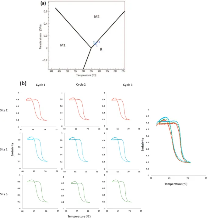
It is largely accepted that VO2 undergoes a first order phase
transition from a semiconducting monoclinic M1 to a metallic Rutile (R) phase. Recent studies, have however firmly established the formation of a second monoclinic phase, M2, as an intermediate between M1 and R[19,20]. Although the formation of M2 phase is not detectable by infrared imaging, spatial Raman mapping re-ported earlier[13], we have shown that certain regions of the film undergo the M1-M2-R transition pathway whereas other regions undergo a direct M1 to R transition. The transition temperature (Tc)
as indicated inFig. 4a when compared/superposed on to the VO2
stress-phase diagram[20]evidences the presence of tensile stress
in the films and implies the formation of the M2 intermediate phase. It is generally possible to generate a stress map starting from the temperature-dependent thermal imaging.
Fig. 4b compares the thermal emissivity hystereses extracted from various restricted surface areas of a few
mm
2(referred to as site 1, 2 & 3). The thermal emissivity at the microscopic scale re-veals significant differences in the transition temperature reaching up to 0.3 K. In contrast, measuring successive hystereses at the same restricted areas shows no measurable difference and the curves cannot be discerned from each other. This observation brings further evidence to the involvement of the stress field dis-tribution and its relation with the robust memory effect. Despite the surface heterogeneity, the memory effect enables a perfect reversibility of thermally controlled thermal emissivity asFig. 4. (a) Transition temperature measured by an IR camera at three different restricted sites are marked over the strain-phase transition diagram[20]of VO2revealing the strained
nature of the films. (b) Emissivity versus temperature curves for the three sites over multiple temperature cycles shows no change what so ever in between successive cycles. Whereas upon comparing Ɛ vs T curves for all sites together, we notice a minor difference in the peak emissivity and the Tc.
measured at the macroscopic scale.
VO2metamaterial coatings offer a superior flexibility compared
to traditional cermet coatings which feature fixed distribution and density of metal particles. Guo et al.[21]described how metallic inclusions can be engineered to tailor matter-light interaction. Authors reviewed the applications of metallic nanostructures for light trapping in solar energy-harvesting structures and devices from thin film photovoltaic cells to solar thermal structures[21]. Therefore, by controlling the size, shape and density of metallic inclusions, VO2coatings clearly place themselves as an attractive
and versatile all-oxide alternative. Tuneable emissivity provides a fertile ground for the design and integration of innovative smart light modulation functionalities in existing technologies.
Fig. 5displays emissivity tuning by adjusting the cooling and heating cycles in the metamaterial region. By limiting the extent of cooling to the temperature enabling the maximal emissivity (marked by a blue circle inFig. 5b) and beginning the heating stage in the subsequent cycle (Fig. 5c), it is possible to take benefit of the observed emissivity spike to further enhance the amplitude of the emissivity change. The described control of temperature ramp yields tuneable emissivity of VO2metamaterial between 0.94 and
0.1.Fig. 5bef highlight the possibility to adjust the emissivity be-tween 0.1 and virtually any intermediate value, %0.94, by appro-priately selecting the minimal cooling temperature. Similar approach can be implemented to enable emissivity change be-tween 0.94 and virtually any intermediate value, &0.1, by appro-priately selecting the maximal heating temperature. The memory effect enables in our study adjusting and maintaining the system at specific values of emissivity. Therefore, the temperature is a reliable parameter to precisely control the overall cermet architecture.
Other heating-cooling cycles can be conveniently designed to adjust both the minimal and maximal emissivity values within the 0.1e0.94 range. As the semiconductor to metal transition of VO2
occurs in picosecond time scale[22,23], a high-speed light modu-lator can be designed.
Thermally controlled switching of emissivity in VO2 films is
demonstrated inFig. 6a. Initially VO2films are stabilized at a steady
temperature of 68!C in the metallic state with low emissivity. A
programmed transient temperature dip (cooling pulse) of
DT ¼ 1.5
!C drives the system to switch from a low emissivity stateat Ɛ ¼ 0.1 to a high emissivity state at Ɛ ¼ 0.94. A programmed transient temperature increase (heating pulse) of similar amplitude drives the system back to the low emissivity state. This way, VO2in
the disordered metamaterial state can be used as an optical switch with controlled emissivity that correlates directly with the infrared reflection. Therefore, the smart cermets can be explored for appli-cations as a shutter and IR light modulation. A contrasting trig-gering profile in Fig. 6b highlights the versatility of switching patterns. By maintaining the system at a steady temperature in the middle of the hysteresis loop, emissivity switching is achieved by providing tiny temperature pulses in either direction. Small energy inputs lead to large changes in emissivity, thereby making them highly efficient and low power consuming alternatives to existing emissivity control devices.
Coatings, exhibiting emissivity control and infrared modulation require micro fabrication and additional processing challenges like multilayer deposition, MEMS fabrication and patterning
[8,11,24e26], all of which increase the complexity and cost of the end product. Due to the intrinsic property of VO2 coatings, no
additional processing or patterning steps are required to achieve
Fig. 5. Variable emissivity as shown from (a) to (f) is achieved by adjusting the minimal temperature of cooling cycle, and beginning the heating cycle immediately. Precise emissivity state can be reached by manipulating the cooling and heating temperatures.
light modulation. High
D
Ɛis achieved by providing small temper-ature pulses. These changes in emissivity are in fact a direct consequence of the variation in the topography of metallic in-clusions in VO2metamaterial state. Hence a modular and tuneableemissivity state is reached by changing the size, shape and density of metal inclusions into a semiconducting matrix thus functioning as a smart cermet. We believe it is the first time VO2 films are
suggested to act as smart cermet.
In conclusion, smart cermet concept was introduced using VO2
films in the metamaterial temperature range. VO2in particular and
correlated oxides with SMT in general, can be ideal candidates for future light modulation, infrared reflectivity and thermal emissivity control to name a few. In this article, the optical modulation in VO2
is thermally triggered. Electrical field[27]or mechanical stress[28]
can also be implemented for the actuation of the SMT in VO2.
Combining this strongly responsive material property with existing and upcoming technologies opens up countless possibilities to integrate innovative functionalities in light modulation and solar energy harvesting.
Appendix A. Supplementary data
Supplementary data related to this article can be found at
https://doi.org/10.1016/j.mtphys.2017.12.002.
References
[1] F. Cao, K. McEnaney, G. Chen, Z. Ren, A review of cermet-based spectrally selective solar absorbers, Energy Environ. Sci. 7 (2014) 1615e1627. [2] J. Moon, T.K. Kim, B. VanSaders, C. Choi, Z. Liu, S. Jin, R. Chen, Black oxide
nanoparticles as durable solar absorbing material for high-temperature concentrating solar power system, Sol. Energy Mater. Sol. C 134 (2015) 417e424.
[3] C.A. Arancibia-Bulnes, C.A. Estrada, J.C. Ruiz-Su!arez, Solar absorptance and thermal emittance of cermets with large particles, J. Phys. D Appl. Phys. 33 (2000) 2489e2496.
[4] H. Krishnamoorthy, Z. Jacob, E. Narimanov, I. Kretzschmar, V. Menon, Topo-logical transitions in metamaterials, Science 336 (2012) 205e209.
[5] J. Zhou, X. Chen, J. Guo, Efficient thermal-light interconversions based on optical topological transition in the metal-dielectric multilayered meta-materials, Adv. Mater. 28 (2016) 3017e3023.
[6] H. Wang, L. Wang, Perfect selective metamaterial solar absorbers, Opt. Express 21 (106) (2013) 1078e1093.
[7]X. Liu, T. Tyler, T. Starr, A.F. Starr, N.M. Jokerst, W.J. Padilla, Taming the blackbody with infrared metamaterials as selective thermal emitters, Phys. Rev. Lett. 107 (2011) 045901.
[8]T.D. Swanson, MEMS Device for Spacecraft Thermal Control Applications, United States patent US 6,538,796, 2003.
[9]J. Meseguer, I. P!erez-Grande, A. Sanz-Andr!es, Spacecraft Thermal Control, Elsevier, 2012.
[10] D. Hengeveld, M. Mathison, J. Braun, E. Groll, A. Williams, Review of modern spacecraft thermal control technologies, HVAC&R Res. 16 (2010) 189e220. [11] H. Demiryont, D. Moorehead, Electrochromic emissivity modulator for
spacecraft thermal management, Sol. Energy Mater. Sol. C 93 (2009) 2075e2078.
[12] M.M. Qazilbash, M. Brehm, B.G. Chae, P.C. Ho, G.O. Andreev, B.J. Kim, S.J. Yun, A.V. Balatsky, M.B. Maple, F. Keilmann, H.T. Kim, Mott transition in VO2 revealed by infrared spectroscopy and nano-imaging, Science 318 (2007) 1750e1753.
[13] S. Kumar, F. Maury, N. Bahlawane, Electrical switching in semiconductor-metal self-assembled VO2 disordered metamaterial coatings, Sci. Rep. 6 (2016) 37699.
[14] M.A. Kats, R. Blanchard, S. Zhang, P. Genevet, C. Ko, S. Ramanathan, F. Capasso, Vanadium dioxide as a natural disordered metamaterial: perfect thermal emission and large broadband negative differential thermal emittance, Phys. Rev. X 3 (2013) 041004.
[15] M.A. Kats, D. Sharma, J. Lin, P. Genevet, R. Blanchard, Z. Yang, M.M. Qazilbash, D.N. Basov, S. Ramanathan, F. Capasso, Ultra-thin perfect absorber employing a tunable phase change material, Appl. Phys. Lett. 101 (22) (2012) 221101. [16] D.M. Douglas, T. Swanson, R. Osiander, J. Champion, A.G. Darrin, W. Biter,
P. Chandrasekhar, Development of the variable emittance thermal suite for the space technology 5 microsatellite, AIP Conf. Proc. 608 (2002) 204e210. [17] H. Demiryont, D. Moorehead, Electrochromic emissivity modulator for
spacecraft thermal management, Sol. Energy Mater. Sol. Cells 93 (12) (2009) 2075e2078.
[18] N. Vardi, E. Anouchi, T. Yamin, S. Middey, M. Kareev, J. Chakhalian, Y. Dubi, A. Sharoni, Ramp-reversal memory and phase-boundary scarring in transition metal oxides, Adv. Mater. 29 (21) (2017), 1605029.
[19] J. Cao, Y. Gu, W. Fan, L.Q. Chen, D.F. Ogletree, K. Chen, N. Tamura, M. Kunz, C. Barrett, J. Seidel, J. Wu, Extended mapping and exploration of the vanadium dioxide stress-temperature phase diagram, Nano Lett. 10 (7) (2010) 2667e2673.
[20] J.H. Park, J.M. Coy, T.S. Kasirga, C. Huang, Z. Fei, S. Hunter, D.H. Cobden, Measurement of a solid-state triple point at the metal-insulator transition in VO2, Nature 500 (2013) 431e434.
[21] C.F. Guo, T. Sun, F. Cao, Q. Liu, Z. Ren, Metallic nanostructures for light trapping in energy-harvesting devices, Light Sci. Appl. 3 (4) (2014) e161.
[22] Z. Zhai, Z. Li, Y. Xiao, Q. Shi, L. Zhu, W. Huang, Q. Peng, Ultrafast THz modu-lation characteristics of photo-induced metal-insulator transition of W-doped VO2film, in: 40thInternational Conference on Infrared, Millimeter, and Ter-ahertz Waves (IRMMW-THz), 2015, 1e1.
[23] O.L. Muskens, L. Bergamini, Y. Wang, J.M. Gaskell, N. Zabala, C.H. De Groot, D.W. Sheel, J. Aizpurua, Antenna-assisted picosecond control of nanoscale phase transition in vanadium dioxide, Light Sci. Appl. 5 (2016), e16173. [24] J. Rensberg, S. Zhang, Y. Zhou, A.S. McLeod, C. Schwarz, M. Goldflam, M. Liu,
J. Kerbusch, R. Nawrodt, S. Ramanathan, D.N. Basov, Active optical meta-surfaces based on defect-engineered phase-transition materials, Nano Lett. 16 (2016) 1050e1055.
[25] H. Kocer, S. Butun, E. Palacios, Z. Liu, S. Tongay, D. Fu, K. Wang, J. Wu, K. Aydin, Intensity tunable infrared broadband absorbers based on VO2phase transition using planar layered thin films, Sci. Rep. 5 (2015) 13384.
[26] H. Demiryont, Emissivity-modulating electrochromic device for satellite thermal control, SPIE News-Room 10 (2008) 1e2.
[27] A. Crunteanu, M. Fabert, J. Cornette, M. Colas, J.C. Orlianges, A. Bessaudou, F. Cosset, Electricfield-assisted metal insulator transition in vanadium dioxide thin films: optical switching behavior and anomalous far-infrared emissivity variation, Proc. SPIE (2015), 93640J.
[28] J.I. Sohn, H.J. Joo, D. Ahn, H.H. Lee, A.E. Porter, K. Kim, D.J. Kang, M.E. Welland, Surface-stress-induced Mott transition and nature of associated spatial phase transition in single crystalline VO2 nanowires, Nano Lett. 9 (2009) 3392e3397.