Pépite | Procédés technologiques pour l’électronique flexible à base de graphène
190
0
0
Texte intégral
(2) Thèse de Wei Wei, Lille 1, 2015. Acknowledgement Foremost, I would like to express the deep and sincere appreciation to my supervisor Prof. Henri HAPPY for continuous support of my Ph.D study and research, for his patience, kindness, expertise and excellent guidance. Without his supervision and constant help, it would not have been possible for me to finish this doctoral thesis. I am grateful to my co-directors Dr. E. Pallecchi and Dr. E. Pichonat, who guide my research work in cleanroom and assist me when I write this thesis. Without their help, it is also impossible to obtain the results that I presented in this thesis. Particularly, I give my deep appriciation to Dr. D. Vignaud, who gave me valuable discussions and sincere help during all my PhD study. My sincere thanks also goes to Dr. D. Mele, Mr. B. Moez, Mr. M. Khenissa, Dr. X. Zhou and Dr. J. Thielleux, who introduce me and help me to the device fabrication work in cleanroom, and the microwave characterization of the graphene filed effect transistors. Their help are so important and it ensures the high efficiency of my work. Mr. M. Colin helped me for the 3-D image of our device structure and I highly appreciate his help. Because my work has deep cooperation with other groups, I am also grateful to them. They are: professor C. Luxey and his group; professor L. Tuami and his group for making inkjet printing devices. They are: Dr. G. Deokar, Dr. K. Haechon and company of Graphenea for supporting the high quality graphene and optimizing the graphene transfer process. I would also like to express my gratitude to all of the engineers in cleanroom who helped me in many ways. They are Mr. M. Francois; Mr. F. Vaurette ; Mr. Y. Deblock; Mr. P. Tilmant; Ms. C. Legrand; Mr. B. Grimbert; Ms. A. Fattorini; Ms. E. Galopin; Mr. M. Dewitte; Ms. I.R. Jeune and Ms. C. Brillard. The engineers in microwave characterization center, who are Ms. V. Avramovic; Mr. E. Okada and Ms. S. Lepilliet.. © 2015 Tous droits réservés.. doc.univ-lille1.fr.
(3) Thèse de Wei Wei, Lille 1, 2015. I would like to thank my reviewers: Professor. M. Mouis and Professor. A. Shukla for their great contribution to review this dissertation and thank Professor. D. Pavlidis; Professor. P. Legagneux; Professor J. Dayen and Professor G. Dambrine for participating in my final defense committee. I have also to thank all my friends in IEMN who helped me. They are Colin, Theo, Moez, Mohamed, Sarah, Marina, Ewa, Pierre, Nadine, Philipp.Latzel, Philippe Altuntas, Adrien, Natalia, Chong, Jinshan, Justine, Valeria, Jorge, Alain, and I spent a pleasant time with them. We had a rich memory together. Last but not the least, I would like to thank my family: my parents and my wife. They give me all the supports and love, which endows me power for moving forward.. © 2015 Tous droits réservés.. doc.univ-lille1.fr.
(4) Thèse de Wei Wei, Lille 1, 2015 Table of Content. Table of Content General Introduction. 3. Chapter I Inkjet printing of microwave passive components. 7. I.1 Introduction .................................................................................................... 7 I.2 Inkjet printing technology .............................................................................. 9 I.2.1. Inkjet printing working principle ....................................................... 9. I.2.2. Description of printing equipment: Dimatix Fujifilm inkjet printer .. 9. I.2.3. Substrates ......................................................................................... 12. I.2.4. Ink .................................................................................................... 14. I.3 Parameters optimization of the inkjet printing on flexible substrate ........... 16 I.3.1. Firing voltage ................................................................................... 16. I.3.2. Pattern design ................................................................................... 18. I.3.3. Wettability ........................................................................................ 21. I.3.4. Ink of Suntronic U5603, sintering and resistivity ............................ 23. I.4 Realization of printed microwave devices ................................................... 30 I.4.1. Coplanar wave guide (CPW) transmission line ............................... 30. I.4.2. Coplanar square monopole antenna ................................................. 40. I.4.3. Structures for thermal conductivity measurement ........................... 44. Conclusion of Chapter I ....................................................................................... 47 References of Chapter I ....................................................................................... 48. Chapter II On rigid substrates: bottom gate Graphene Field Effect Transistor with dielectric of natural oxide 53 II.1. Introduction ................................................................................................ 53. II.2. Description of graphene and graphene transistor ....................................... 54 II.2.1 Graphene properties ......................................................................... 54 II.2.2 Field effect transistors based on graphene ....................................... 57 II.2.3 Graphene synthesis .......................................................................... 62. II.3. Process technology for bottom gate GFETs with natural oxide as dielectric 74 II.3.1 Layout design ................................................................................... 75 II.3.2 Electron-Beam lithography .............................................................. 75 II.3.3 GFET fabrication process ................................................................ 78. II.4 Physical and electrical characterization ...................................................... 89 1 © 2015 Tous droits réservés.. doc.univ-lille1.fr.
(5) Thèse de Wei Wei, Lille 1, 2015 Table of Content. II.4.1 Graphene mobility ........................................................................... 89 II.4.2 Graphene contact resistance ............................................................. 93 II.4.3 GFETs characterization .................................................................. 106 Conclusion of Chapter II .................................................................................... 124 References of Chapter II .................................................................................... 126. Chapter III On flexible substrates: bottom gate graphene field effect transistor with dielectric of natural oxide 134 III.1 Introduction ............................................................................................. 134 III.2 General description of flexible GFET ..................................................... 135 III.3. Device fabrication process and graphene characterization on Kapton. substrate. .................................................................................................... 138. III.3.1 Optimization of alignment process ................................................ 139 III.3.3 Device fabrication process ............................................................. 141 III.4. Characterization of material and contact resistance .............................. 146 III.4.1 Graphene mobility on Kapton substrate ........................................ 146 III.4.2 Graphene contact resistance ........................................................... 147. III.5. Characterization of GEFTs devices ....................................................... 149 III.5.1 DC Characterization when substrate is flat .................................... 149 III.5.2 Small-signal high frequency characteristics when substrate is flat 153 III.5.3 GFET characterization when substrate is bended .......................... 156 III.5.4 Thermal effect from substrate ........................................................ 159. Conclusion of Chapter III .................................................................................. 163 Reference of Chapter III .................................................................................... 164. General conclusion and Perspective. 167. Publications list. 170. Appendix I. 172. Appendix II. 174. Appendix III. 177. Appendix IV. 182. Appendix V. 184. 2 © 2015 Tous droits réservés.. doc.univ-lille1.fr.
(6) Thèse de Wei Wei, Lille 1, 2015 General Introduction. General Introduction Flexible electronics has drawn growing attention for the past several years due to its numerous potential applications. The relevant research relies on the existence of suitable fabrication technologies and novel materials. The objective of my PhD work is to develop devices based on flexible substrates. There are mainly two parts involved: (i) passive devices (transmission lines, antenna, etc) fabricated by inkjet printing technology; (ii) Graphene field effect transistors (GFET) fabricated by conventional electron-beam lithography. In chapter 1, we show how to utilize inkjet printing technology to fabricate passive devices on flexible substrates and the characterization of these devices. Inkjet printing is a promising fabrication technology for flexible electronics due to the advantages of being low cost, mask-free process, waste reduction and compatible with arbitrary substrate. The challenge of this technology is the quality and reliability of printed patterns in terms of geometry. In this work, we firstly present the work of optimizing inkjet printing technology based on Dimatix printer equipment, commercial ink from Suntronic (U5603 - silver nanoparticles based solution) and commercial flexible substrates, KAPTON and PEN. After optimization, we are able to print patterns with well controlled geometry. Some microwave passive devices such as coplanar wave guide and antenna were fabricated. For RF characterization, the device performances were explored with flat (without strain) or bent (strained) substrates. We show that inkjet printing technology has promising potential for flexible electronics. In chapter 2, we discuss the field effect transistors based on graphene material on rigid substrates. Graphene, a two-dimensional carbon based material, has attracted attentions due to its unique electronic properties. Additionally, the truly two-dimensional nature and strong mechanical property makes graphene very suitable for flexible electronics. In our work, we present the fabrication and characterization of GFETs on rigid substrates. The bottom gate structure using aluminium as metal gate is chosen. The GFET dielectric is formed by the natural oxide of aluminium. This approach is used to avoid conventional atomic layer deposition method, which needs high temperature. Chemical vapor deposition grown graphene on copper foil is adopted, and transferred using an optimized wet transfer process. The high quality monolayer graphene is preserved both after graphene transfer and device fabrication process. Contact resistance is explored by using different transmission line model structures. The transistors with different geometry (gate length of 100, 200 and 300 nm combining with gate width of 12, 24 and 50 µm) is characterized by both static and 3 © 2015 Tous droits réservés.. doc.univ-lille1.fr.
(7) Thèse de Wei Wei, Lille 1, 2015 General Introduction. dynamic measurements. In chapter 3, we discuss the fabrication and characterization of graphene field effect transistors on flexible substrates. By using almost the same fabrication process on rigid substrates, we successfully fabricate GFETs on a flexible substrate, kapton. Pure Au is used to form contact metal and low contact resistance is obtained. The transistors with different geometry (gate length of 100, 200 and 300 nm and width of 12, 24 and 50 µm) are characterized by both static and dynamic measurements. We report as measured current gain cut-off frequency ( ft-DUT ,without any de-embedding) of 39 GHz and maximum oscillation frequency (fmax) of 13.5 GHz in devices with 100 nm gate length and 12 µm gate width. To our knowledge, these results reach to the state of the art for flexible GFET. Moreover, the evaluation of RF performances for different substrate bending radius (strain varying from 0% to 0.5%) is discussed and the thermal dispersion of substrate in channel region for different drain source bias is explored. The results presented in chapter 3 further demonstrate the great potential of our process for graphene based flexible electronics.. 4 © 2015 Tous droits réservés.. doc.univ-lille1.fr.
(8) Thèse de Wei Wei, Lille 1, 2015 Inkjet printing of microwave passive components. Chapter I Inkjet printing of microwave passive components. 5 © 2015 Tous droits réservés.. doc.univ-lille1.fr.
(9) Thèse de Wei Wei, Lille 1, 2015 Table of Content-Chapter I. Table of Content-Chapter I Chapter I Inkjet printing of microwave passive components. 7. I.1 Introduction .................................................................................................... 7 I.2 Inkjet printing technology .............................................................................. 9 I.2.1. Inkjet printing working principle ....................................................... 9. I.2.2. Description of printing equipment: Dimatix Fujifilm inkjet printer .. 9. I.2.3. Substrates ......................................................................................... 12. I.2.4. Ink .................................................................................................... 14. I.3 Parameters optimization of the inkjet printing on flexible substrate ........... 16 I.3.1. Firing voltage ................................................................................... 16. I.3.2. Pattern design ................................................................................... 18. I.3.3. Wettability ........................................................................................ 21. I.3.4. Ink of Suntronic U5603, sintering and resistivity ............................ 23. I.4 Realization of printed microwave devices ................................................... 30 I.4.1. Coplanar wave guide (CPW) transmission line ............................... 30. I.4.2. Coplanar square monopole antenna ................................................. 40. I.4.3. Structures for thermal conductivity measurement ........................... 44. Conclusion of Chapter I ....................................................................................... 47 References of Chapter I 48. 6 © 2015 Tous droits réservés.. doc.univ-lille1.fr.
(10) Thèse de Wei Wei, Lille 1, 2015 Inkjet printing of microwave passive components. Chapter I Inkjet printing of microwave passive components I.1 Introduction Printed electronics is a set of printing methods for depositing electronic materials (insulating, conducting, and semiconducting) onto arbitrary substrates to create a wide range of devices, such as organic thin film transistors (OTFTs), light-emitting devices (LEDs), diodes, detectors, etc[1-10]. Compared with conventional electronics, printed electronics has attracted attention due to its significant advantages such as compatibility with various substrates (flexible, transparent and low cost substrates, such as paper), low temperature processing, and no requirement for vacuum processing[11-14]. Printed electronics has become a growth industry that already has generated significant revenue. Source from Organic Electronics Association (OE-A) manifests that the sales of products including printed electronics were 23-24 billion US $ in the year of 2014, and future annual growth rates of 20% were predicted.( as shown in Figure I-1).. Figure I-1: Evolution of printed/organic electronics market [15] Inkjet printing is a promising fabrication technology for flexible electronics. However, improving the quality and the reliability of printed patterns in terms of geometry and resolution remains challenging. It means, the printed pattern dimensions must be as close as possible to the designed value, and the pattern defects such as holes and the rough pattern boundary must be well controlled. This chapter is oriented to the printing technology for design and fabrication of flexible radio frequency (RF) components. At this frequency range, the geometry of 7 © 2015 Tous droits réservés.. doc.univ-lille1.fr.
(11) Thèse de Wei Wei, Lille 1, 2015 Inkjet printing of microwave passive components. devices has high impact on their performances. The objective of this chapter is to use printing technology to fabricate devices with well controlled geometry. In this work, the inkjet printing technology has been chosen as fabrication technique. Therefore, in the first part of this chapter, I will describe the printing equipment (Fujifilm Dimatix printer) and printing principal associated with commercial silver nanoparticles ink (SunTronic U5603) and flexible substrates of PEN and Kapton. The process optimization will be described in appendix I while the main results will be shown in main text. In second part, based on optimized printing parameters, the structures of CPW transmission lines with nice printing quality were realized. The RF characterization of these transmission lines combining the considerations of geometric dimensions, sintering temperature, and substrate bending will be presented. For CPW lines on KAPTON, the loss lower than 0.4 dB/mm up to 40 GHz was obtained, which shows possibility to design RF circuits using this technique. Also, it has been found that the RF performance of the CPW lines on KAPTON is minimally affected by substrate bending. Besides, two collaboration works about antenna printing and three omega method structures printing will be shortly presented, which both further indicate the potential of our work for flexible electronics. Figure I-2 shows two examples of printed achievements in this work: (a) is a pattern of IEMN shaped by array of droplets on PEN substrate; (b) shows a bended Kapton substrate on which the CPW transmission lines with different dimensions have been fabricated by inkjet printing. The study of this new technology was completed in the beginning of my PhD thesis.. Figure I-2: Examples of some printed results by Dimatix in this work, (a) Pattern of IEMN shaped by array of droplets on PEN substrate; (b) CPW transmission lines on Kapton substrate. 8 © 2015 Tous droits réservés.. doc.univ-lille1.fr.
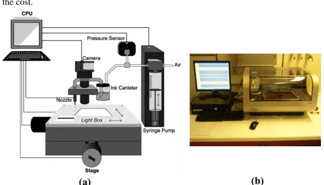
(12) Thèse de Wei Wei, Lille 1, 2015 Inkjet printing of microwave passive components. I.2 Inkjet printing technology I.2.1 Inkjet printing working principle Inkjet Printing is a type of material deposition technique that forms a patterned layer by ejecting ink droplets from a chamber through a hole, called nozzle, onto arbitrary substrates, such as paper, plastic etc. Additionally, an annealing process, or referred as sintering, is necessary to make the ink solvents evaporate leaving a solid layer on the substrate. Figure I-3 (a) shows a typical illustration of inkjet printer, and (b) shows the picture of Fujifilm Dimatix inkjet printer, which is used in this work. The pattern is first designed in a computer, and then is realized by inkjet printing on substrate. Dimatix is based on Drop-on-Demand (DoD) approach[16][17]. All the droplets ejected are directly deposited to the target substrate and form the patterned layer. One major advantage of DoD inkjet printing is that it is a mask-free process, which reduces the cost.. Figure I-3:(a) Illustration of inkjet printer (b) Picture of the Fujifilm Dimatix Materials Printer used in this work, with the screen showing a designed mask.. I.2.2 Description of printing equipment: Dimatix Fujifilm inkjet printer The Dimatix inkjet Printer is a laboratory tool that enables researchers, scientists, and engineers to evaluate the use of ink jetting technology for new manufacturing processes[18-21]. It is designed to be convenient and easy to carry out “proof of concept” 9 © 2015 Tous droits réservés.. doc.univ-lille1.fr.
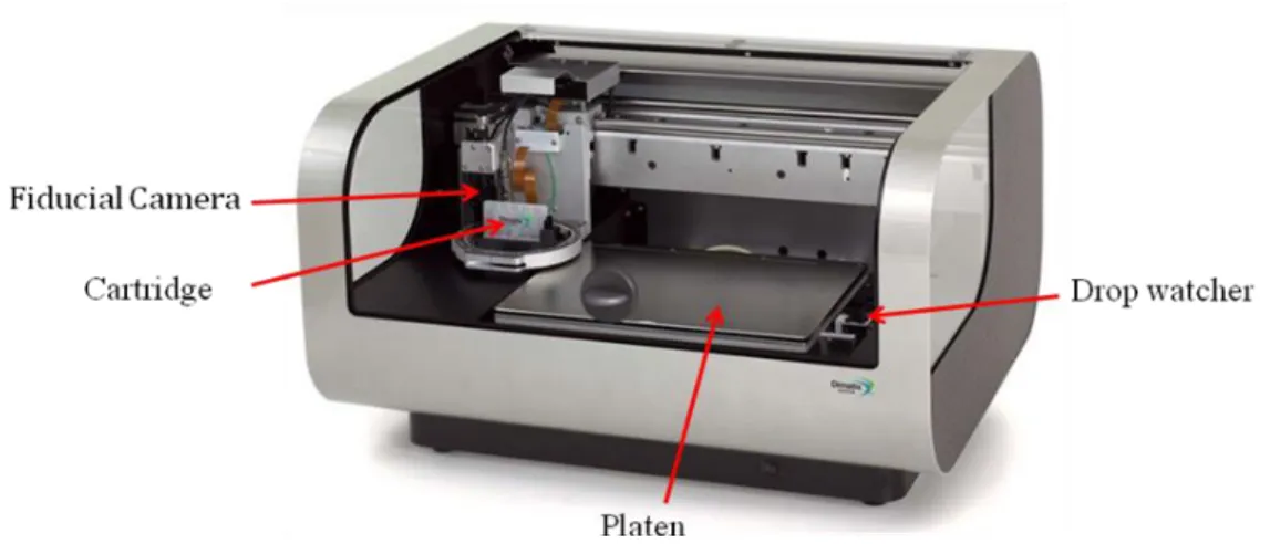
(13) Thèse de Wei Wei, Lille 1, 2015 Inkjet printing of microwave passive components. and development work using inkjet technology. The printer is made up of different components mainly detailed as Figure I-4 shown. -Cartridge. The part which contains ink materials and ejects ink droplet with a certain formation setting, see more details below section of printing principle. -Platen. A turntable surface to maintain substrate for printing. It has a vacuum system to maintain flexible substrate as flat. -Drop watcher. A camera to observe droplet formation in real time. It provides important information, such as, stability, volume and speed of as printed droplets, and by which different parameters could be determined. -Fiducial Camera. A camera right above the as printed substrate with two main functions: first, to select position where printing originates and also align the pattern position before printing, and second, to verify the printing result after fabrication process.. Figure I-4:Picture of the Fujifilm Dimatix Materials Printer. I.2.2.1 Cartridge description As Figure I-5 (a) shows, with 16 identical nozzles beneath, the cartridge is filled with ink. Each nozzle has been connected with a tube through which the ink is allowed to pass. On one side of the tube a piezoelectric element can be found to induce pressure and depression inside the tube, because this piezoelectric element has shape deformation according to various voltage applied on it. Therefore, by setting different voltage value and their duration time, which is named as waveform parameter (or as drop formation), the jetting process would be accordingly formed. Typically, waveform is divided into four segments, as shown is Figure I-5 (b). Each segment has three properties: duration, level and slew rate. Duration and slew rate are two parameters linked with jetting frequency, which can be defined for inks with different viscosity. Additionally, slew rate can also define the velocity of droplet ejected from nozzle. 10 © 2015 Tous droits réservés.. doc.univ-lille1.fr.
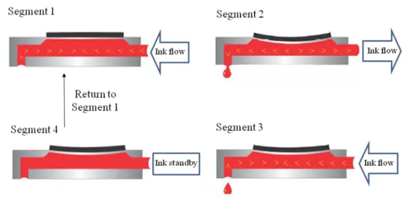
(14) Thèse de Wei Wei, Lille 1, 2015 Inkjet printing of microwave passive components. Level parameter is used to define the volume of one jetted droplet, and it reflects how much the piezoelectric element would be deformed while duration and slew rate reflects how fast the piezoelectric element verifies.. Figure I-5: (a) picture of a cartridge and (b) simplified schematic of waveform for ejection voltage Figure I-6 gives more details about droplet ejecting process. In segment 1, which is the beginning of an ejecting pulse, a negative voltage makes the piezoelectric element back to a relaxed or straight position from depressed state of segment 4, and the chamber with its maximum volume have the ink pulled in. In segment 2, a main drop ejection phase, the chamber would be compressed by the piezoelectric element with its maximum level and the output pressure would generate a droplet ejected. In segment 3, a recovery phase, the voltage would be set back down and piezoelectric element decompresses a bit to have ink refilled into chamber again. In addition, the pulling back force in this segment is also helping to break off the droplet ejected in previous segment. In segment 4, zero voltage moves the piezoelectric element back to its original position in preparation for segment 1 again. To this end, a cycle of droplet ejecting has been finished.. 11 © 2015 Tous droits réservés.. doc.univ-lille1.fr.
(15) Thèse de Wei Wei, Lille 1, 2015 Inkjet printing of microwave passive components. Figure I-6: Schematic of four-segment voltage waveform of the piezoelectric crystal It is clear now that by verifying the parameters of these four segments: duration, level and slew rate, different drop formation for different viscosity liquid can be obtained. It should he noted that during the printing process, a clean nozzle without clotting by some particles in solution based ink is critical to the head performance. To avoid the cases of blocked fluid path, DMP2800 has a special nozzle cleaning treatment, purging. As a maintenance function, purging will apply air pressure to outside of fluid bag to force ink through entire fluid path and out all nozzles promptly. Therefore, purging is an inevitable action for an error free jetting process.. I.2.3 Substrates Among the flexible substrates, the properties of PET, PEN and Kapton have retained our attentions for RF application. Figure I-7 represents an image of commercial version of the three substrates, as well as their monomer formulation. Table I-1 provides the thermal, physical and electrical properties of these three substrates.. 12 © 2015 Tous droits réservés.. doc.univ-lille1.fr.
(16) Thèse de Wei Wei, Lille 1, 2015 Inkjet printing of microwave passive components. Figure I-7: Image of substrate PET, PEN and Kapton with their monomer formulation Thermal property is a crucial parameter to be considered by engineers during the fabrication process. One can find that Kapton is more suitable for applications which require higher temperature since it has the highest melting point and the lowest shrinkage. For this reason Kapton was selected for my thesis. Among the physical properties, surface roughness has an important role on determining the morphology of the patterns that can be printed on the surface. PEN features the lowest roughness, with 0.6 nm, therefore it was also used in this thesis. The electrical properties of the substrate are important when the substrates are used for electric devices[22][23]. For example, the resistivity needs to be very high for radio frequency application. From an electronics point of view, the three substrates are relatively similar with high resistivity and a dielectric constant varying between 2.9 and 3.5.. 13 © 2015 Tous droits réservés.. doc.univ-lille1.fr.
(17) Thèse de Wei Wei, Lille 1, 2015 Inkjet printing of microwave passive components. Table I-1: Main Properties of PET, PEN and Kapton substrates Properties. PET. PEN. Kapton. Shrinkage,at 150 ºC (%). 1.5. 0.4. 0.17. Melting Temperaure,Tm(ºC). 258. 269. 410. Glass transition temperature,Tg(ºC). 110. 155. 360. Surface roughness(nm). 0.8. 0.6. 5. Youngs Modulus, at 150 ºC (GPa). 1. 3. 2. Dielectric Constant. 3.1. 2.9. 3.5. Resistivity (Ω·cm). 1016. 1015. 1017. Thermal. Physical. Electrical. I.2.4 Ink One key component of the printing technology is the ink[24-26]. The properties of the ink depend on the specific printing technique. Generally, the printable solution-based ink for piezoelectric nozzles must have properties listed below: . Surface tension between 28 to 33 dynes/cm, an important parameter to determine its contact angle on a certain substrate.. . Viscosity between 10 to 30 cps, directly affecting waveform as mentioned previously.. . Low evaporation rate after printing, thus solvent with high boiling point is preferable.. . Nano-particles uniformly dispersed in solution without aggregating each other.. In this study, we use a commercial ink, Suntronic U5603, which has 20wt% Silver nanoparticles with ethanol based solution, in addition with ethanediol(10-20wt%) and glycerol(5-10wt%). The datasheet of this product shows a surface tension of 27-31 dynes/cm and viscosity of 10-13 cps at 25ºC. Importantly, regardless of the formation method of inks, the sintering process is always necessary to remove the solvent and surfactant layer on surface of nanoparticles. 14 © 2015 Tous droits réservés.. doc.univ-lille1.fr.
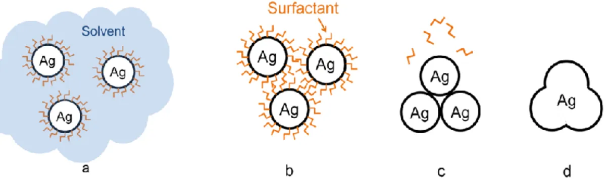
(18) Thèse de Wei Wei, Lille 1, 2015 Inkjet printing of microwave passive components. The metallic nanoparticles dispersed in solvent have large surface curvature, i.e., very high surface energy due to the large surface-to-volume ratio, they tend to aggregate. In further, the direct contact between individual nanoparticles in the aggregation may lead to merging behavior, and subsequently, to a larger cluster. All these bigger particles can be threats to printing stability or even to cause nozzle clotting. Therefore, to have a stable and uniform dispersion in solution, the nanoparticles have to be modified on their surfaces to avoid aggregation. Figure I-8 illustrates different status of metallic nanoparticles (taking silver as an example here) from dispersing in ink solvent to form densified and conductive bulk layer. With surface modification, a protection shell, or referred as surfactant will be present on each nanoparticles to avoid nanoparticles aggregation[14], as Figure I-8 (a) shows. The solvent evaporation will occur right after inkjet printing, which renders the particles close together, shown in Figure I-8 (b). Nevertheless, the surfactant layer, usually some non-conductive organics, even as thin as few nanometers, is still sufficient to prevent electrons moving from one particle to another [27]. To have direct physical contacts between nanoparticles, typically, the surfactant can be removed by an increase in temperature. In low temperature range, the nanoparticles began to lose their organic shell and partly contact physically, as Figure I-8 (c) depicted. In this phase, due to the reduction of surface energy as driving force for sintering, the necks between particles begin to form. As temperature increased, all the organic materials will be burnt off and necks area will further increase, leaving a more condensed structure as depicted in Figure I-8 (d).. Figure I-8: Simplified schematic of sintering process of silver nanoparticles In this study, with consideration of commercial ink Suntronic U5603, we performed experiments for the effect of two factors, sintering temperature and sintering time, on the morphologies and electrical resistivity of printed pattern. Relative results will be presented in section I.3.3.. 15 © 2015 Tous droits réservés.. doc.univ-lille1.fr.
(19) Thèse de Wei Wei, Lille 1, 2015 Inkjet printing of microwave passive components. I.3 Parameters optimization of the inkjet printing on flexible substrate The previous paragraph highlights the general information about printing principle, substrates (especially PEN and Kapton) properties, and the thermal sintering treatment of nanoparticles-based ink. Particularly, we explained the formation process of one droplet from ink cartridge to substrate through nozzles, which is a critical part of inkjet printing technique. Various electrical components with different structures realized by inkjet printing on flexible substrate have been reported in literature[15]. These studies demonstrate the possibility of realizing microwave circuit by inkjet printing technology. However, improving the quality and the reliability of printed patterns in terms of geometry and resolution remains a major challenge. Briefly speaking, for electrical components fabricated by inkjet printing, such as coplanar wave guide (CPW) transmission line, there are four important criteria which will finally determine the printed device performance: 1) as low as possible the mismatch between printed and designed pattern; 2) well controlled pattern defects ( holes, cracks and rough pattern boundary); 3) minimum printable distance between two separated tracks; 4) a sufficiently low resistivity of the pattern. In details, to meet the four criteria as mentioned in last paragraph, there are several parameters concerning to Dimatix equipment, substrate and ink which are possible to be optimized. In this section, we will give the optimized printing parameters by showing the good results. Although many works has been done in optimization, the details of parameters optimization will not appear in the main text, but be presented in annexes.. I.3.1 Firing voltage As mentioned previously, waveform is consisted of four segments to have one droplet ejected. The voltage amplitude of second segment, referred as firing voltage, is regarded as a main parameter in waveform. Two aspects of the droplet ejection, volume and velocity of the as ejected droplet, would be effectively controlled by firing voltage. An increased value of firing voltage results in both larger volume and higher velocity of as-ejected droplet. We find that a high firing voltage and thus high jetting velocity destroys the completeness of the droplet shaped on substrate. As Figure I-9 (a) shows, in high firing voltage range (30~40V), the formation of droplets with good shape 16 © 2015 Tous droits réservés.. doc.univ-lille1.fr.
(20) Thèse de Wei Wei, Lille 1, 2015 Inkjet printing of microwave passive components. becomes difficult. The jetting velocity as a function of firing voltage is plotted in Figure I-9 (b). The droplet jetting velocity can be obtained directly from Dimatix manipulate software. We find that for ink of SunTronic U5603, jetting velocity in range from 4 to 12 m/s (firing voltage from 16 V ~ 25 V) is preferable to obtain droplets with good shape.. Figure I-9: (a) Optical image of droplets formed on PEN by three different firing voltage (20, 30 and 40 V); (b) jetting velocity as a function of firing voltage As shown in Figure I-10, with the firing voltage of 16 V, arrays of droplets with intact round shape are formed on substrates of PEN and Kapton. The diameters of the droplets on these two substrates are slightly different: 38 µm for PEN and 47 µm for KAPTON. It indicates the surface tension of PEN and KAPTON should be slightly different.. 17 © 2015 Tous droits réservés.. doc.univ-lille1.fr.
(21) Thèse de Wei Wei, Lille 1, 2015 Inkjet printing of microwave passive components. Figure I-10: Droplets formation on substrates of PEN in (a) and KAPTON in (b), both by firing voltage of 16V. I.3.2 Pattern design In pattern design, a Dimatix software based computer work, we can create and modify printing patterns. There is a very important parameter in terms of smooth pattern control, drop spacing, which gives the centre to centre distance from one droplet of ink to another adjacent in X and Y direction, as what Figure I-11 (a) shows. Figure I-11 (b) shows a part of the real design of a rectangular shaped pattern in Dimatix software.. Figure I-11: (a) Schematic diagram of drop spacing and (b) a real design in Dimatix software The final pattern geometry is strongly determined by drop spacing. The optimization work of drop spacing is provided in Appendix I, in which the pattern geometry depending on different drop spacing values is carefully explored on PEN (we don’t show the details of optimization of printing patterns on Kapton, because of the identical process as presented for PEN). Because the droplet diameter on PEN and Kapton are different, the optimized drop spacing values are also different accordingly. 18 © 2015 Tous droits réservés.. doc.univ-lille1.fr.
(22) Thèse de Wei Wei, Lille 1, 2015 Inkjet printing of microwave passive components. Therefore, we have normalized the drop spacing by dividing the droplet diameter, so that the ratio of drop spacing over droplet diameter can be regarded as a universal reference for pattern geometry control. Table I-2 shows the remarks of pattern geometry obtained from different ratio of drop spacing over droplet diameter. Note that these results are based on many tests as shown in appendix I from both on PEN and Kapton substrates. Table I-2: Lines smooth control depending on the ratio of drop spacing over droplet diameter Drop spacing /Droplet Diameter. Smooth control comment Lines will be continuous, but bulging phenomenon and. < 0.6. wave-like boundary are often observed Good range to obtain continuous lines with smooth. ~ 0.7. boundary control Although the smooth boundary control is good, but the. > 0.8. lines are highly risk to be not continuous. Figure I-12(a) shows a line pattern printed on PEN. The jetting voltage used is 20V, and drop spacing of 28 µm is used to keep ratio of drop spacing over droplet diameter around 0.7. Figure I-12(b) shows the thickness of the line, which has been measured by profile meter from point A to B as illustrated in Figure I-12 (a). Note that the scale of the thickness is nanometer and that of the width is micrometer. A standard thermal sintering process is explored prior to thickness measurement so that the ink solvent is removed.. 19 © 2015 Tous droits réservés.. doc.univ-lille1.fr.
(23) Thèse de Wei Wei, Lille 1, 2015 Inkjet printing of microwave passive components. Figure I-12: (a) optical image of a line printed on PEN by 20V jetting voltage; (b) thickness measurement from point A to B as illustrated in (a) The minimum printable distance between two separated tracks is another challenge for inkjet printing technology. In this work, Dimatix is capable to print two separate patterns either in one time printing (the two patterns belong to one design file) or in two times printing (the two patterns belong to two different design file). The reproducible minimum distance between two patterns of around 17µm is obtained in this work by one time printing method, as shown in Figure I-13.. 20 © 2015 Tous droits réservés.. doc.univ-lille1.fr.
(24) Thèse de Wei Wei, Lille 1, 2015 Inkjet printing of microwave passive components. Figure I-13:patterns printed on PEN with a reducing gap, the minimum separation between two patterns of 17µm is obtained On substrate of Kapton, with the optimized parameter obtained on PEN, the same printing. results. are. obtained.. To. this. end,. we. have. discussed. about. equipment-dependent parameters: firing voltage and drop spacing. Next section will focus on the properties of the ink and also its interaction with substrate.. I.3.3 Wettability Wettability is normally used to describe how a liquid maintain its contact with a solid substrate which results from a balance between adhesive and cohesive forces. This balance, in Yong’s equation: γSL + γLG cos θ = γSG , equals the balance of surface tension between the three phases: solid, liquid and gas[17]. From Figure I-14 we see a contact angle θ which provides us important information of wettability as it is determined by the balance of those three phases surface tension.. Figure I-14: Schematic for Yong’s equation and contact angle The surface tension of a substrate is determined by either the material or temperature of the substrate. [28]. . Taking PEN as an example, to verify the wettability 21. © 2015 Tous droits réservés.. doc.univ-lille1.fr.
(25) Thèse de Wei Wei, Lille 1, 2015 Inkjet printing of microwave passive components. evolution of Suntronic U5603 ink on PEN substrate with different surface tension, we separately deposit single droplets on different PEN substrates which are already baked up to 25ºC, 70ºC, 110ºC and 150ºC, respectively. Figure I-15 shows the contact angle measurements of these single droplets. Supposing surface tension of ink is a constant value, deduced from Yong’s equation, we believe that the variation of contact angle from 12.3ºto 28.1ºare resulted from different surface tension of PEN caused by different substrate temperatures. It is concluded that ink of Suntronic U5603 shows the best wettability on PEN substrate at room temperature(around 25ºC). In further, the effect of wettability on pattern formation is studied. Figure I-16 shows a line pattern printed on PEN substrate with 25 ºC in (a) and with 70 ºC in (b). We observe that the printed line pattern on PEN with temperature of 25 ºC exhibits good boundary control, and a uniform line without holes or bulging is obtained. However, line pattern printed on PEN with temperature of 70 ºC shows a quite worse boundary control, and non-uniform line was observed due to the high contact angle.. Figure I-15: contact angle variation on substrate of PEN with its different temperature. Figure I-16: One line printed on PEN with substrate temperature of 25°C, in (a) where a line with good geometry has been obtained; and of 70°C in (b), where a poor shaped line has been formed 22 © 2015 Tous droits réservés.. doc.univ-lille1.fr.
(26) Thèse de Wei Wei, Lille 1, 2015 Inkjet printing of microwave passive components. I.3.4 Ink of Suntronic U5603, sintering and resistivity I.3.4.1 Realization measurement. of. Van. der. Pauw. structures. for. resistivity. Several sintering methods have been reported for inkjet printing technology, such as microwave, laser and thermal sintering[29-36]. The conventional thermal sintering method has been used in this work. Van der Pauw method has been used for resistivity measurement. Van der Pauw patterns has been printed on silicon wafer and sintered at different temperature. HL5500PC with four tips platform was used for measurement. Below, details of Van der Pauw fabrication by inkjet printing and resistivity extraction will be provided. Based on that, the effect of sintering temperature and time on resistivity will be explored. Van der Pauw method is widely applied for resistivity and mobility measurement of two-dimensional materials. More details of measurement principle will be provided in Chapter2. The goodness of this technology lies in a highly accurate measurement which thus requires a symmetrical pattern with contacts located on the circumference. Figure I-17 (a) shows the Van der Pauw pattern designed mask in Dimatix software. The pattern consists of one square shape (width of w), the measurement area, with four contacts on each of its corner where to place the probes. Totally, squares with three different dimensions (w=1, 1.25 and 1.5 mm) have been designed and printed. As Figure I-17 (b) shows, no holes, pattern defects, or inhomogeneous parts could be found in the printed Van der Pauw pattern (w=1 mm), which satisfies the Van der Pauw conditions.. 23 © 2015 Tous droits réservés.. doc.univ-lille1.fr.
(27) Thèse de Wei Wei, Lille 1, 2015 Inkjet printing of microwave passive components. Figure I-17: (a) Van der Pauw pattern designed in Dimatix; (b) optical image of the Van der Pauw pattern after printing; (c) measured thickness of Van der Pauw pattern followed the trace of AB as illustrated in (b) Figure I-17 (c) shows the Van der Pauw pattern thickness measured by profile meter. We observe a relative flat surface except for a bit thicker edge area caused by coffee ring effect. Coffee ring effect describes the phenomenon that during the evaporation of a droplet, the liquid evaporates faster from interior to the edge. In this study, after 30 min @150℃ sintering treatment, we find about 1300 nm thickness for edge and 900 nm for the rest area. In such case, the average thickness for the whole area would be calculated for resistivity measurement. For statistic, five patterns for each Van der Pauw dimension (x=1, 1.25 and 1.5 mm) have been printed. And with sintering conditions of 30 min @150℃, Figure I-18 shows the resistivity obtained by Van der Pauw measurement for different pattern dimension.. 24 © 2015 Tous droits réservés.. doc.univ-lille1.fr.
(28) Thèse de Wei Wei, Lille 1, 2015 Inkjet printing of microwave passive components. Figure I-18: Resistivity obtained from Van der Pauw pattern with pattern length of 1mm, 1.25 mm and 1.5 mm. I.3.4.2 Effect of sintering temperature on resistivity Several Van der Pauw patterns with identical dimensions (side length of 1.5mm) were inkjet printed on five Si/SiO2 substrates, respectively. Under ambient condition, five samples were separately heated up to 100℃, 125℃, 150℃, 175℃ and 200℃ on hot plate with heating rate of 15℃/min from room temperature. After having reached to target temperature, 30 min of duration with the target temperature and then a cooling down at 20℃/min were followed. Sheet resistance (R□) was directly measured by using Van der Pauw method, and resistivity(ρ) was calculated by taking into account the pattern thickness(t) as given by formula (ρ= R□· t). Figure I-19 shows the electrical resistivity variations of Suntronic U5603 as a function of sintering temperature. Scanning electron microscopy (SEM) images in Figure I-20 shows the morphology and particle packing within the printed patterns after different sintering temperature. Figure I-21 shows the silver nano-particle size distribution obtained by SEM image analysis.. 25 © 2015 Tous droits réservés.. doc.univ-lille1.fr.
(29) Thèse de Wei Wei, Lille 1, 2015 Inkjet printing of microwave passive components. Figure I-19: Dependence of patterns resistivity on different sintering temperatures As shown in Figure I-19, in the beginning with sintering temperature of 100℃, the resistivity is still relatively high. Probably in this early stage the organic protective shell are still not completely removed and the neck formation is not effectively started. Confirmed by Figure I-20 and particles size distribution analysis in Figure I-21, the silver nanoparticles with a typical diameter 20 to 50 nm can still be distinguished individually. As the sintering temperature increased up to 150℃, more organic materials would be removed and the coalescence of Ag nanoparticles begin to occur due to a tendency to minimize the overall surface area of particles. Confirmed by SEM image of Figure I-20, many of the particles are connected to each other while some still keep their shapes and are not fully connected yet. The resistivity drastically drops from 76 μΩ·cm to 34 μΩ·cm, according to 100℃ and 150℃ respectively. This improvement of resistivity indicates that conduction path between the particle is established by inter particle neck formation. Good agreement can also be found in Figure I-21 which shows an increased diameter of 40-70nm for Ag nanoparticles after 150℃ sintering.. 26 © 2015 Tous droits réservés.. doc.univ-lille1.fr.
(30) Thèse de Wei Wei, Lille 1, 2015 Inkjet printing of microwave passive components. Figure I-20: SEM images of patterns cross section sintered by 100℃, 150℃ and 200℃ for 30 min Further increasing the sintering temperature up to 200℃ reveals an even lower resistivity of 11.6 μΩ·cm, which is about 8 times higher than the theoretical value of bulk silver. It is also noticed that the resistivity decrease rate from 150℃ to 200℃ is much smaller than that from 100℃ to 150℃. Probably because in this stage, the organic materials have been burned off already, and only the neck formation between nanoparticles contributes the resistivity decrease. A clear particle shape change from discrete-and spherical particles to continuous-and sintered particles could be observed in Figure I-20, particles begin to merge into larger agglomerates and these increased three-dimension continuous network structures explain the further drop of resistivity. The typical nanoparticles diameter distributes in the range of 40 to 120 nm after 200℃ sintering are shown in Figure I-21.. 27 © 2015 Tous droits réservés.. doc.univ-lille1.fr.
(31) Thèse de Wei Wei, Lille 1, 2015 Inkjet printing of microwave passive components. Figure I-21: Particle size distributions for patterns with different sintering temperatures,100°C in (a), 150°C in (b) and 200°C in (c),which are obtained by SEM image analysis (inset SEM image shows the typical nanoparticle morphology according to different sintering temperature). I.3.4.3 Effect of sintering time on resistivity Similar to the effect of sintering temperature discussed in above paragraph, the effect of sintering time on ink of Suntronic U5603 was studied in terms of resistivity. Several Van der Pauw patterns with identical dimensions (side length of 1.5mm) were inkjet printed on six Si/SiO2 substrates, respectively. Under ambient condition, six samples were all heated up to 200 °C on the hot plate with heating rate of 30 ℃/min from room temperature but separately remains for 10, 20, 30, 40, 50 and 60 min. Then a cooling down at the rate of 40 ℃/min was followed. The resistivity as a function of sintering time (sintering temperature of 200°C) is shown in Figure I-22. After the pattern was annealed for 10 min, the resistivity significantly drops to a value of 19±3 μΩ·cm. It means probably all the chemical part in the ink has been burned off in the first 10min. As the sintering time increases to 20 min, the resistivity reaches to 12±1 μΩ·cm. However, after sintering time of 30min, the resistivity value remains quite stable. It indicates that after 30 min sintering the neck formation between particles should be almost finished and we can conclude that 30 min is the effective 28 © 2015 Tous droits réservés.. doc.univ-lille1.fr.
(32) Thèse de Wei Wei, Lille 1, 2015 Inkjet printing of microwave passive components. sintering time.. Figure I-22:Resistivity of patterns as a function of the sintering time with a fixed sintering temperature of 200℃. 29 © 2015 Tous droits réservés.. doc.univ-lille1.fr.
(33) Thèse de Wei Wei, Lille 1, 2015 Inkjet printing of microwave passive components. I.4 Realization of printed microwave devices I.4.1 Coplanar wave guide (CPW) transmission line CPW is a type of electrical transmission line which can be applied to convey high frequency signals with minimum reflections and power loss.[37] It consists of three metal strips placed on the same side of a dielectric substrate. Figure I-23 shows the schematic of a CPW line. The central line with width W, conveys microwave signals while the two other metal lines separated from the central line on each side with a small gap of S are ground plane, or return conductor. Both central line and ground plane have the identical thickness, t, and length, L, approached by a simultaneous fabrication.. Figure I-23: Three-dimensional schematic of CPW transmission line with geometric parameters. I.4.1.1 Fabrication process of inkjet printing In this study, CPW transmission line were both inkjet printed on substrate of PEN and KAPTON. in previous section, we find that the diameters of the droplets on these two substrates are different: 38 µm for PEN and 45 µm for KAPTON. It indicates the surface tension of PEN and KAPTON should be slightly different from each other. Therefore, accordingly the printing parameters applied on PEN would be distinguished to that on KAPTON. Table I-3 shows the optimized printing parameters for both these two substrates.. 30 © 2015 Tous droits réservés.. doc.univ-lille1.fr.
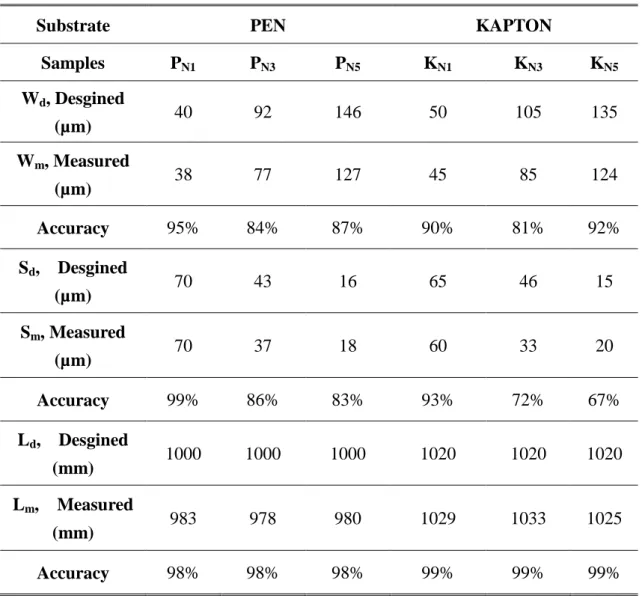
(34) Thèse de Wei Wei, Lille 1, 2015 Inkjet printing of microwave passive components. Table I-3: Printing parameters used for printing CPW transmission lines on both PEN and KAPTON substrates Firing. Drop. Jetting. Substrate. Sintering. voltage. space. frequency. temperature. treatment. (V). (µm). (KHz). (°C). (min & °C). PEN. 16. 27. 3. 25. KAPTON. 16. 30. 5. 25. Substrate. 30min @150 °C 30min @200 °C. Resistivity (µΩ·cm ) ~20 ~11. CPW transmission line with six different geometry dimensions have been designed in Dimatix software in terms of central line width W, gap S to the ground plane, and length L. Note that the length of Pad are not taken into account when we design and measure the length L. In these six different geometric structures, by using the optimized printing parameters, three were realized on PEN (PN1, PN2 and PN3) and another three were realized on KAPTON (KN1, KN2 and KN3). Figure I-24 (a) shows the design in Dimatix software with different value of W and S, and Figure I-24 (b) and (c) show the optical images of these lines obtained on PEN and Kapton.. Figure I-24: CPW structures in (a) mask design; (b) obtained on PEN; and (c) obtained on Kapton (1) CPW on PEN Figure I-25 shows the patterns of PN1, PN2 and PN3 obtained on PEN. From zoomed-in images, we can see that the minimum value of 18 µm for S has been achieved thanks to the optimized printing parameters. In further, we don’t find any 31 © 2015 Tous droits réservés.. doc.univ-lille1.fr.
(35) Thèse de Wei Wei, Lille 1, 2015 Inkjet printing of microwave passive components. defects such as holes or cracks. The as printed patterns are quite homogeneous and continuous, and a very good boundary control has been obtained. Table I-4 shows the printing results, which include the information of dimensions and the printing accuracy by comparing the structure dimensions of both designed and measured. Note that the dimensions of W, S and L have been illustrated in Figure I-23.. Figure I-25: Optical images of PN1, PN2 and PN3 CPW lines on PEN, with zoomed-in images where the values of W and S are marked. (2). CPW on Kapton Figure I-26 shows the patterns of KN1, KN2 and KN3 obtained on Kapton. From. zoomed-in images, we can see that the minimum value of 20 µm for S has been 32 © 2015 Tous droits réservés.. doc.univ-lille1.fr.
(36) Thèse de Wei Wei, Lille 1, 2015 Inkjet printing of microwave passive components. achieved. The printed structures with good quality (patterns are homogeneous and continuous) are also obtained. Table I-4 shows the printing results, which includes the information of dimensions and the printing accuracy by comparing the structure dimensions of both designed and measured.. Figure I-26: Optical images of KN1, KN2 and KN3 CPW lines on Kapton, with zoomed-in images where the values of W and S are marked. 33 © 2015 Tous droits réservés.. doc.univ-lille1.fr.
(37) Thèse de Wei Wei, Lille 1, 2015 Inkjet printing of microwave passive components. Table I-4:Summary of CPW transmission lines printing results on both PEN and KAPTON substrates Substrate Samples Wd, Desgined (µm) Wm, Measured (µm) Accuracy Sd,. Desgined (µm). Sm, Measured (µm) Accuracy Ld, Desgined (mm) Lm,. Measured (mm). Accuracy. PEN. KAPTON. PN1. PN3. PN5. KN1. KN3. KN5. 40. 92. 146. 50. 105. 135. 38. 77. 127. 45. 85. 124. 95%. 84%. 87%. 90%. 81%. 92%. 70. 43. 16. 65. 46. 15. 70. 37. 18. 60. 33. 20. 99%. 86%. 83%. 93%. 72%. 67%. 1000. 1000. 1000. 1020. 1020. 1020. 983. 978. 980. 1029. 1033. 1025. 98%. 98%. 98%. 99%. 99%. 99%. Accuracy: (1- |measured value – designed value| / designed value) x 100 (%). I.4.1.2 RF Characterization of CPW transmission lines printed on both PEN and KAPTON when substrate is flat In this work, for RF measurement of CPW transmission line fabricated by inkjet printing, what we want to know are the characteristic impedance Zc and attenuation constant α, which can be both extracted from S-parameters measurement, appendix II gives more details. The measurement is finished by another PhD student Moez, and the relative explanation will be given in his thesis. The measurements have been carried out using an HP8510C precision network (10MHz-40GHz) analyser (PNA) connected to the Cascade ground-signal-ground probes. The LRRM calibration technique was performed to shift the reference plan up to the probe tips by using an impedance-standard-substrate (ISS) from the probes manufacturer. Afterward, the 34 © 2015 Tous droits réservés.. doc.univ-lille1.fr.
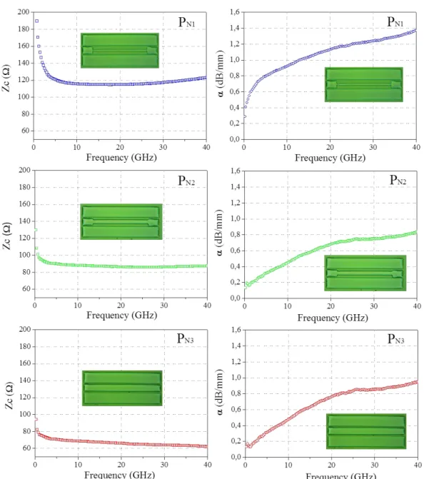
(38) Thèse de Wei Wei, Lille 1, 2015 Inkjet printing of microwave passive components. corresponding S-parameters of CPW transmission lines on both PEN and KAPTON were measured from 0.025 to 40 GHz. From the as measured S-parameters, the Zc and α were extracted. Below, for the CPW transmission lines on both PEN and KAPTON, the characteristic impedance and attenuation constants will be presented. (1) Zc and α of CPW on PEN Figure I-27 shows the characteristic impedances versus frequency for P N1, PN2 and PN3. In frequency range up to Giga hertz, the characteristic impedances can be L. expressed as zc = √C , because the imaginary part becomes prominent and the real part can be negligible. Both C and L are highly dependent of the geometry of CPW transmission lines, especially the ratio of gap-to-central line width (S/W). This explains that for samples of PN1, PN2 and PN3 with different S/W ratio, different Zc were obtained, as shown in Figure I-27. Figure I-27 also shows the attenuation constant versus frequency for PN1, PN2 and PN3. Up to 40 GHz, the attenuation is found to be about 1.3 dB/mm, 0.8 dB/mm and 0.9 dB/mm for PN1, PN2 and PN3 respectively.. 35 © 2015 Tous droits réservés.. doc.univ-lille1.fr.
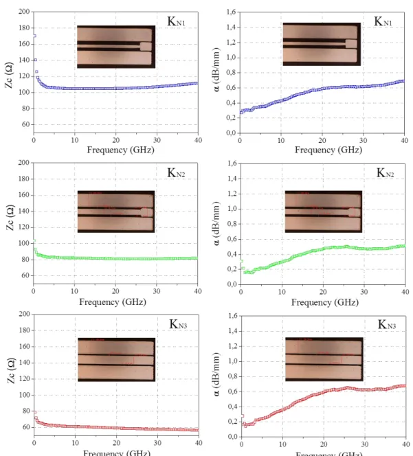
(39) Thèse de Wei Wei, Lille 1, 2015 Inkjet printing of microwave passive components. Figure I-27: Characteristic impedance Zc and attenuation constant α of samples PN1,PN2 and PN3 on PEN substrate (2) Zc and α of CPW on KAPTON Similar to the discussion on PEN, Figure I-28 shows the characteristic impedances versus frequency for KN1, KN2 and KN3. Figure I-28 also shows the attenuation constant versus frequency for KN1, KN2 and KN3. Up to 40 GHz, the attenuation is found to be about 0.7 dB/mm, 0.5 dB/mm and 0.7 dB/mm for KN1, KN2 and KN3 respectively. We believe that the less loss obtained from CPW lines on KAPTON comparing to that on PEN comes from the lower resistivity of CPW lines on KAPTON which thanks to the higher sintering temperature (see Table I-3).. 36 © 2015 Tous droits réservés.. doc.univ-lille1.fr.
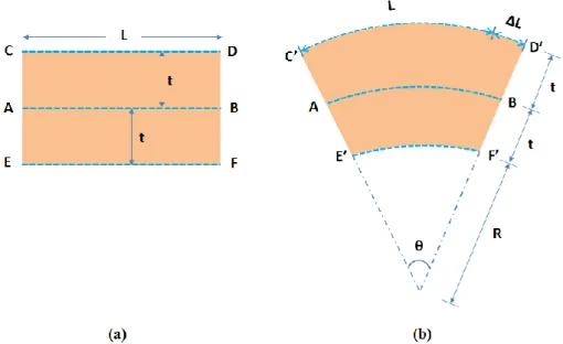
(40) Thèse de Wei Wei, Lille 1, 2015 Inkjet printing of microwave passive components. Figure I-28:. Characteristic impedance ZC and attenuation constant α of samples KN1, KN2 and KN3 on KAPTON substrate. I.4.1.3 Effect of substrate strain on attenuation constant (1) Strain calculation of bended substrate Since the flexible electronics is one major application for inkjet printing technology, the relative bending measurement needs to be developed. To analyse the mechanism of the bending layer in our substrate, the model from Chiang. [38]. is used. here. For a simple case that the flexible substrate is composed by only single material, Figure I-29 (a) shows the substrate cross section with thickness of 2t. Before bending, in each layer of the substrate the lengths are identical: CD=AB=EF. Let’s define the layer CD, AB and EF are in the top, middle and bottom positions of the substrate 37 © 2015 Tous droits réservés.. doc.univ-lille1.fr.
(41) Thèse de Wei Wei, Lille 1, 2015 Inkjet printing of microwave passive components. respectively. When the flexible substrate is bended on a supporter with radius of R, as shown in Figure I-29 (b), layer AB will keep its original length L and all the layers above AB will be stretched while those below it will be compressed. Because of this, the layer of AB is named as neutral layer (NL). The strain value of CD layer is defined by: ∆𝑙. 𝜀 = 𝐿,. (I-1). where L is the original length and ΔL is the change of length after bending. In the case illustrated in Figure I-29, the strain of CD layer becomes: 𝜀=. 𝐶 ′ 𝐷 ′ −𝐶𝐷 𝐴𝐵. =. 𝜃(𝑅+2𝑡) 𝜃(𝑅+𝑡). 𝑡. − 1 = 𝑅+𝑡, (I-2) t. In most cases, R ≫ t, so the strain can be estimated as ε ≈ R. From this equation, we can conclude that thicker substrate thickness t or smaller bending radius R can both yield higher value of strain on the bending surface.. Figure I-29: Illustration of one single-material film cross section of (a) before bending and (b) after bending on supporter with radius R (2) Evolution of attenuation constant with different substrate strain As an important nature of flexible electronics, microwave measurement based on KAPTON substrate being bended on supports with radius curvature of 25 mm and 15 mm were carried out. The strain calculation using the method discussed above gives strain value of 0.5% and 0.3% for 15 mm and 25 mm radius supports. Figure I-30 (a) shows the flat and bended measurement. All the measurement results discussed before were based on this flat measure. After, the substrate was fixed onto bended support. To guaranty the measurement is adapted to this bending system, the substrate was bended 38 © 2015 Tous droits réservés.. doc.univ-lille1.fr.
(42) Thèse de Wei Wei, Lille 1, 2015 Inkjet printing of microwave passive components. along the Z direction of a CPW line (Figure I-23). In this way, the centre and ground must be in the same plane for putting the RF tips. Figure I-30 (b) shows the measured attenuation constant versus frequency corresponding to strain of 0, 0.3 % and 0.5% from sample KN3. One can see that almost negligible difference could be found when the CPW line was bended with strain of 0.3 % and 0.5%. It indicates that the inkjet printed CPW lines possess very stable performance after bending, so that the CPW lines could be fully utilized without degrading the performance.. Figure I-30: Illustration of Kapton substrate under different strain with RF probes in (a) and evolution of the attenuation constant versus frequency based on different strain in (b). I.4.1.4 Effect of sintering temperature on attenuation constant Because KAPTON has excellent thermal stability, we also studied the effect of sintering temperature on attenuation in the range of more than 200℃. Three KN3 CPW lines were inkjet printed on KAPTON with the same printing parameters discussed above, so that the same dimension could be obtained. Afterward, these three lines were sintered at 200℃, 250℃ and 300℃ for 30 min, respectively. Figure I-31 shows the evolution of the attenuation constant versus frequency for these three KN5 lines. Losses smaller than 0.3 dB/mm at 40 GHz is obtained after sintering treatment of 300℃, and this improvement is believed to be the result of a higher conductivity. It is worth to mention that 0.2 dB/mm at 40 GHz achieves the same order of attenuation from CPW lines fabricated by photolithography with the same dimension but with a 350 nm thick gold deposited by metal evaporation.. 39 © 2015 Tous droits réservés.. doc.univ-lille1.fr.
(43) Thèse de Wei Wei, Lille 1, 2015 Inkjet printing of microwave passive components. Figure I-31: Comparison of attenuation constant for sample KN3 sintered by temperature of 200℃, 250℃ and 300℃, respectively. I.4.2 Coplanar square monopole antenna I.4.2.1 Fabrication process of inkjet printing on PEN substate Several circuits and antennas have been realized on flexible substrates with inkjet technology for applications at frequency below 10 GHz, such as RFID tags or sensor systems[39-41], however no antenna fabricated by inkjet printing technology on flexible substrate with characterization up to 60 GHz has been fully presented. This work has been done with a collaboration of a group in University of Nice (Leat Group). We are in charge of structures fabrication. Note that the dimensions of the antenna are required for good precision because the performance is highly dimension-dependent.. 40 © 2015 Tous droits réservés.. doc.univ-lille1.fr.
(44) Thèse de Wei Wei, Lille 1, 2015 Inkjet printing of microwave passive components. Figure I-32: Top view of the layout of the antenna To obtain antenna patterns with accurate dimensions and also to have good boundary control, we have made many tests with different printing parameters until the best optimized parameters have been achieved (Table I-5). Particularly, this antenna design has several different components, such as patch, feed line and ground plane and the dimensions are differing from each other. Here, we used different firing voltages and drop space for these components according to different dimensions. With these optimized parameters which we believe are very suitable for this structure design, the final antenna has been printed, as shown in Figure I-33 and all the critical dimensions have been measured and compared with design values as presented in Table I-6. From Figure I-33, as-printed patterns are found to be homogeneous and continuous. The precision report in Table I-6 also indicates the quality and accuracy of our inkjet process. Table I-5: Optimized printing parameters for printing antenna on PEN substrate. Parameters. Values. Firing. Drop. Jetting. Substrate. voltage. space. frequency. temperature. (V). (µm). (KHz). (°C). 16~25. 20~25. 3. 25. Sintering treatment. Resistivity. (min. (µΩ·cm). @ °C) 30min @150 °C. ~20. 41 © 2015 Tous droits réservés.. doc.univ-lille1.fr.
(45) Thèse de Wei Wei, Lille 1, 2015 Inkjet printing of microwave passive components. Figure I-33: Optical image of (a) the antenna fed by a 400 µm GSG probe (b) zoomed-in of red marked area. 42 © 2015 Tous droits réservés.. doc.univ-lille1.fr.
(46) Thèse de Wei Wei, Lille 1, 2015 Inkjet printing of microwave passive components. Table I-6: Summary of dimension performance for antenna Accuracy. Designed value. Measured value. Vd (mm). Vm (mm). Htop. 1.12. 1.124. 99.4%. Hbot. 1.27. 1.255. 99%. Wgroud. 0.195. 0.204. 95.4%. Lslot. 1.8. 1.808. 99.6%. Gslot. 0.2. 0.197. 98.5%. Lpatch. 1.4. 1.401. 99.9%. W. 0.15. 0.152. 98.7%. G. 0.018. 0.019. 95%. Demensions. 100 −. |Vm −Vd | Vd. d(%). I.4.2.2 The gain of antenna Figure I-34 gives the simulated and measured gain of the coplanar square monopole versus frequency in the (φ, θ) = ( 0°, 90°) direction. The total realized gain is found to be higher than 0 dB in the range of 50 to 62 GHz. The very good agreement between simulation and measurement results demonstrates the quality of inkjet fabrication process in this work. The relative work has been published, and a comment from one reviewer is quoted as “a very good technology push” in this work.. Figure I-34: Simulated (dashed line) and measured (plain line ) total realized gain patterns at 60 GHz versus frequency. 43 © 2015 Tous droits réservés.. doc.univ-lille1.fr.
(47) Thèse de Wei Wei, Lille 1, 2015 Inkjet printing of microwave passive components. I.4.3 Structures for thermal conductivity measurement I.4.3.1 Fabrication process of inkjet printing on polyimide substrate Thermal conductivity is an important issue to be considered especially for the applications of flexible electronics, in which the polymer materials are commonly used as substrate, such as polyimide (PI) etc. Three omega method is one of the methods to measure thermal conductivity of solid or soft materials but with accuracy and simpleness. Nevertheless, the structure fabrication is still challenging due to the limitations of conventional technique of lithography, such as time consuming, costly and poor compatibility with arbitrary polymer substrates caused by using different chemical products during the process. Therefore, inkjet printing offers another alternative fabrication method and was first time, to our best knowledge, applied to deposit metallic line on polymer substrate for three omega method measurement. The three omega method requires a metallic line, deposited on the surface of the sample to be tested, which serves as a heater and a temperature sensor. The thermal conductivity can be experimentally extracted from some analysis based on metallic resistance fluctuations when passing through alternating current.As shown in Figure I-35 (a), the metallic line with a certain length of L and width of 2b has two contact pads. To make fair comparison, six metallic lines were fabricated: three by conventional photolithography (lines A, B and C) and another three by inkjet printing (lines 1, 2 and 3).. Figure I-35: Schematic of two pads metallic line with 2b width and l length of (a) original design and (b) Dimatix software design The substrate used in this study is a black opaque polyimide sheet with thickness of 1 mm bought from Goodfellow Company. The challenge for inkjet printing is the relatively high roughness of this polyimide as shown in Figure I-36(a). To obtain a continuous line on such a rough surface, high firing voltage and jetting frequency were found to be preferable after different parameters test, and the final optimized parameters are presented in Table I-7. Figure I-36 (b) shows the metallic line (Au) 44 © 2015 Tous droits réservés.. doc.univ-lille1.fr.
(48) Thèse de Wei Wei, Lille 1, 2015 Inkjet printing of microwave passive components. deposited by photolithography and Figure I-36 (c) shows the metallic line (Ag) fabricated by inkjet printing. As shown in Figure I-36 (b), the smooth boundary control of the printed line is difficult to obtain due to the high surface roughness, and the line width varies between 57 µm and 62µm which yields an average width of around 60 µm. Table I-7: Optimized printing parameters for printing metallic line on polyimide substrate Firing. Drop. Parameters voltage. space. Values. Jetting. Substrate. frequency temperature. (V). (µm). (KHz). (°C). 35. 25. 5. 25. Sintering treatment. Resistivity. (min. (µΩ·cm). & °C) 30min @200 °C. ~11. Figure I-36: (a) Scanning probe microscopy image of a the surface of polyimide and optical image of metallic line on polyimide fabricated (b) by photolithography and (c) by inkjet printing. I.4.3.2 Thermal conductivity Table I-8 summarizes the properties of all the six metallic lines: the width 2b, the length L, the line resistance R, and the thermal conductivity K. We can find that by using three omega method, the thermal conductivity of the metallic lines obtained by inkjet printing technology agrees very well with that of metallic lines prepared by photolithography. The relative work has been published, and we hope this technique will be a promising method for characterization of many polymers that have low chemical resistance.. 45 © 2015 Tous droits réservés.. doc.univ-lille1.fr.
(49) Thèse de Wei Wei, Lille 1, 2015 Inkjet printing of microwave passive components. Table I-8: properties of metallic lines deposited by photolithography and inkjet printing on polyimide substrate Technology Photolithography. Inkjet printing. Line. 2b (µm). L (mm). R (Ω). K (W/m.K). A. 10. 3. 24.253. 0.493. B. 20. 10. 38.806. 0.511. C. 10. 5. 39.651. 0.508. 1. 50. 1. 36.675. 0.517. 2. 60. 2. 39.825. 0.498. 3. 65. 2. 32.838. 0.529. 46 © 2015 Tous droits réservés.. doc.univ-lille1.fr.
(50) Thèse de Wei Wei, Lille 1, 2015 Inkjet printing of microwave passive components. Conclusion of Chapter I Firstly, we have explored the parameters optimization of inkjet printing technology based on Fujifilm Dimatix printer, commercial ink of Suntronic U5603 and substrates of PEN and KAPTON. Printing qualities variations caused by different equipment-dependent parameters were fully presented. We find that in general case, setting the ratio of drop spacing over droplet diameter around 0.7 could give nice printing qualities. Nevertheless, different firing voltage needs to be taken into account for different pattern dimension, and also for the consideration of nozzle jetting conditions. For the commercial ink and substrates of PEN and KAPTON, room temperature on substrate surface during printing is preferable due to the better wettability. The sintering temperature dependent resistivity of the ink Suntronic U5603 was also studied, the resistivity as low as 11.6 μΩ•cm could be achieved by sintering the ink at 200 ℃ for 30 mins. Secondly, for applications based on our optimized printing parameters, different components have been realized. CPW transmission lines with different characteristic impedance on both PEN and KAPTON substrates have been successfully printed with good printing quality. The RF characterizations of these lines combining the considerations of geometric dimensions, sintering temperature, and substrate bending have been performed. For CPW lines on KAPTON, the loss lower than 0.4 dB/mm up to 40 GHz after 300 ℃ sintering was obtained, which is comparable to similar CPW lines fabricated by conventional lithography techniques. Also, we find that the RF performance of the CPW lines on KAPTON is minimally affected by substrate bending. Additionally, two collaboration work about antenna printing and three omega method structures printing have been shortly presented, which both further indicate the promising potential of the optimized inkjet printing technology in this work.. 47 © 2015 Tous droits réservés.. doc.univ-lille1.fr.
Figure
+7
Documents relatifs