To link to this article: DOI: 10.1016/j.matlet.2011.07.082
URL :
http://dx.doi.org/10.1016/j.matlet.2011.07.082
This is an author-deposited version published in:
http://oatao.univ-toulouse.fr/
Eprints ID: 5552
To cite this version:
Laffont , Lydia and Lonjon, Antoine and Dantras, Eric and Demont ,
Philippe and Lacabanne, Colette Optical properties of metallic nanowires
by valence electron energy loss spectroscopy. (2011) Materials Letters,
vol. 65 (n° 23 - 24). pp. 3411-3414. ISSN 0167-577X
O
pen
A
rchive
T
oulouse
A
rchive
O
uverte (
OATAO
)
OATAO is an open access repository that collects the work of Toulouse researchers
and makes it freely available over the web where possible.
Any correspondence concerning this service should be sent to the repository
administrator:
[email protected]
Optical properties of metallic nanowires by valence electron energy loss spectroscopy
L. Laffont
a,⁎
, A. Lonjon
b, E. Dantras
b, P. Demont
b, C. Lacabanne
baCIRIMAT/Institut Carnot, ENSIACET, 4 allée Emile Monso, BP 44362 31030 Toulouse Cedex 4, France
bPhysique des Polymères, CIRIMAT/Institut Carnot, Université Paul Sabatier, 118 route de Narbonne, 31062 Toulouse cedex 9, France
a b s t r a c t
Keywords: Nanoparticles Electron microscopy Optical properties
The determination of intrinsic conductivity of nanowires (NWs) is essential to understand the charge transport behaviour involved in hybrid nanocomposites. These high conductive metallic fillers are good candidate to improve electrical properties of composites in aeronautic industry. The main difficulty is often to achieve the combination of both high spatial resolution and information on the physical properties as electrical conductivity. One of the suitable methods to give the desired information is electron energy loss spectroscopy (EELS) in scanning transmission electron microscopy (STEM) mode, especially in the low-loss region. This is demonstrated by studying the nickel and gold nanowire.
1. Introduction
In the past decade, interest in nanoscale particles grows to pair with the emergence of nanotechnology. It is possible to obtain a wide range of shape and geometry. 1D structure such as nanotubes or nanowires can give conductive applications at nanometric or macroscopic scale by introducing them into a polymer matrix[1–3]. These nanometer-sized objects are good systems to observe the properties of materials at nanometric scale[4–6].
These metallic nanowires (NWs) have to possess a high aspect ratio of nanowires (10–100) to elaborate conductive composites. These com-posite provides electrical percolation threshold for small amount of conductive filler[7–9]and possess the metallic conductivity of their constitutive material[8,10]. These NWs composites are good candidate to aeronautic industry due to their specific properties as mechanical resistivity, hardness, conductivity and magnetic susceptibility. So these low filled conductive composites permit to preserve the mechanical properties of the matrix and to enhance the electrical conductivity of aeronautic composite to prevent the lightning damages or charge accumulation.
Different kind of synthesis permits to obtain metallic nanowires. A controlled growth in solution of a seed of metal achieves nanowires[11]
but the exact geometry of these nanowires is not controlled. The best way to get nanowires with a controlled geometry is to use a substrate called template. This template can be an object with a high aspect ratio such as a CNT coated with metal[12], this method is named positive template. For negative template, the nanowires are prepared by metal plating in a substrate possessing high aspect ratio cavities. Most of the works use anodized aluminum oxide (AAO) membranes[13–15]and
reach good results after the dissolution of the ceramic matrix. This technique was used to obtain the nickel and gold nanowires studied in this work. Direct and reliable measurements of physical properties (such as optical properties) of single NW may not be straightforward because of specific morphologies that make them difficult to handle or because of interactions with neighboring phases, or because of structural changes induced by the process whereby these materials are incorporated into polyphasic materials. Quantitative information on materials properties can be extracted with a good spatial resolution, down to the nanometric range, by exploitation of the low-loss domain of the electron energy loss spectra (EELS).
The purpose of this paper is to determine the intrinsic optical conductivity of single NW by using valence electron energy loss spectroscopy. In fact, VEELS has been often used to determine the physical properties of semi-conductors materials as the band gap, the k value or the optical conductivity [16]. In this contribution, we will demonstrate how the optical conductivity of individual Au and Ni NW can be deduced and the importance on the local determination of conductivity in the specific case of oxidized layer.
2. Experimental 2.1. Materials
Nickel and gold nanowires (NW) were synthesized by electrochem-ical deposition in an anodic aluminium oxide (AAO) porous template. The electrolyte used for nickel deposition was a standard Watts bath with an accurate pH value of 4. Direct current (DC) electrodeposition was carried out at room temperature using a Nickel wire as anode with 1.0 mm in diameter. Gold nanowires (Au NWs) were synthesized by electrochemical deposition in an anodic aluminium oxide (AAO) porous template using free cyanide electrolyte. Direct current (DC) electrode-position was carried out at 50 °C using a gold wire of 1.0 mm in diameter ⁎ Corresponding author.
E-mail address:[email protected](L. Laffont).
as anode. In both case, a porous (AAO) membrane of 200 nm diameter and 50 μm thickness supplied by Whatman was used as template. One side of the AAO membrane was coated with a 35 nm thickness silver layer by using sputtering technique as cathode for electrodeposition. NWs increase was controlled by the time deposition and the direct current intensity using a Keithley 2420 source meter. The AAO membrane was dissolved in NaOH 6 M for 30 min, releasing NWs from the template. Then, NWs were washed with distilled water and filtrated. A following sonication leaded to a very good dispersion of NWs in water or toluene.
2.2. Microstructure
The filtered NWs were stored in acetone and dispersed using an ultrasonic bath. A droplet of this solution was deposited onto a SEM pin. SEM observation was performed using a JEOL JSM 6700F equipped with a field emission gun.
2.3. Optical conductivity of nanowires
The intrinsic optical conductivity of Au and Ni NWs was studied using VEELS. VEELS experiments were carried out using a high resolution Gatan imaging filtering (HRGIF) system in a Tecnai F20 transmission electron microscope equipped with a Wien-filter type monochromator at the National Centre for High Resolution Electron Microscopy (HREM) of Delft University of Technology. A 100 kV operation voltage allowed an energy resolution of 0.50 eV as deter-mined from the full width at half maximum of the zero-loss peak. The following conditions were chosen to acquire the VEELS spectra: an illumination semi-angle α of 2.5 mrd, a collection semi-angle β of 6.5 mrd and an energy dispersion of 0.1 eV/channel. The dielectric function was calculated using the ‘Epsilon’ software performing deconvolution, angular correction, normalization and Kramers-Krönig (KK) transform successively[17]. ‘Epsilon’ is a free software that can be downloaded on
http://pc-web.cemes.fr/espilon/. Prior to any quantitative analysis of the VEELS data, the spectrum was corrected for the point-spread function (PSF) of the instrumentation by a Fourier-ratio deconvolution followed by a Fourier-log deconvolution to eliminate contributions from plural scattering. The material loss function Im(−1/ε(E)) is extracted after angular correction and normalization of the signal using the refractive index (n→∞ for metallic sample). The real part Re(1/ε) is calculated using a KK transform. Re(ε) and Im(ε) are then deduced. So the optical conductivity σ(E) can be deduced[16,18]knowing Im(ε) using the following relation[19]implanted in the Epsilon software[17]: σ(E) = E εoIm(ε)/ħ with ε0: vacuum permittivity and ħ = h/2π (h: Planck constant).
3. Results and discussion
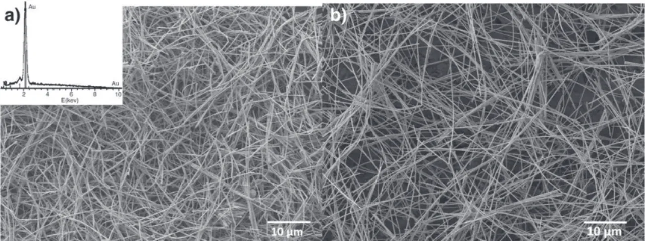
The Au NWs, released from the membrane, are well dispersed in the acetone suspension, as shown in the SEM image inFig. 1a. The Au NWs exhibit a uniform length of 45 μm and a regular diameter of 200 nm. The EDX spectrum was recorded to prove the chemical nature of the Au NWs. The Au peak has the most prominent intensity indicating that the NWs are made up of metallic gold. The weak peaks at low energies reveal the presence of oxygen and aluminium coming from the AAO template. The Au NWs occur individually, no bundles and no sonication-induced damage are observed except for a slight curvature. The Ni NWs exhibit the same characteristic of Au NWs (Fig. 1b), i.e. a uniform length of 45 μm and a regular diameter of 200 nm. These NWs are also well dispersed, no bundles are observed.
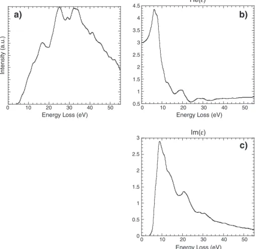
High angle annular dark field (HAADF) image of the Au NWs associated with the VEEL spectrum is presented inFig. 2. A small probe (0.5 nm) was used to acquire all the VEEL spectra for which the shape remains identical along a NW and for different NWs. The dielectric function and the optical conductivity were calculated using the ‘Epsilon'software. Some steps of the low-energy loss signal treatment (single scattering distribution and the Kramers-kronig transformation given Re(ε) and Im(ε)) of Au NWs have shown inFig. 3. The function Im(ε) presents some maxima which correspond to the signature of interband transitions. Since the intensive zero-loss peak hides the fine structure below 1 eV, σ(E) is significant only above 1 eV. Thus, to determine the electrical conductivity at E = 0 eV, the electrical conductivity is extrapolated linearly in the range between 1 and 0 eV starting from 1 eV[16]. Assuming that this extrapolation is correct, the electrical conductivity of Au NW is 72.106S.m− 1. This value is
con-sistent with other observations for bulk (45.106S.m− 1) and with
four-probe measurements on Au NWs[10]. These Au NWs are used for the elaboration of conductive nanocomposite, only 2.2% in vol. is necessary to reach the percolation threshold and to obtain an electrical con-ductivity of 102S/m for the composite.
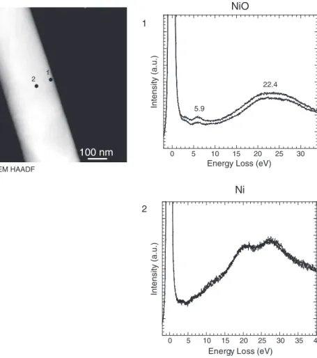
Moreover, various nickel nanowires were synthetized[7]. Physical and chemical treatments were used to completely remove the oxide layer. Nickel nanowires as well as nanoparticles [20]have a large reactivity under atmospheric conditions and a NiO layer cover the nickel core. The conductivity of particles decreases with the raising of NiO surface layer width [20]. After sulphuric acid treatment, TEM study has already shown that a layer of NiO covers Ni NWs[7]. In order to determine the optical conductivity, EELS has been performed on these Ni NWs. VEELS spectra obtained on the surface and the bulk of Ni NWs are shown inFig. 4. These spectra present different signatures that are clearly characteristic of the different compounds (NiO at the edge, Ni at the core in the majority). In fact, the signature of the valence electrons in the low loss region (0–100 eV) can be considered as fingerprint of the
compound, not of the elements. This ‘Epsilon’ analysis permits to extract the real and imaginary part of the dielectric function and to determine the optical conductivity σ(E). These conductivities have been linearly extrapolated from 1 eV to 0 and conductivities of 18.106S/m and 9.106 S/m for Ni and NiO have been obtained. The important conductivity of NiO compared with Ni can be explained by the presence of Ni in the oxide nickel layer due to the analysis[21]. These intrinsic conductivity values are essential to determine the kind of charge transport inside the polymer. These Ni NWs are used for the elaboration of conductive nanocomposite, only 0.75% in volume fraction is necessary to reach the percolation threshold and to obtain an electrical conductivity of 102S/m.
This value is 1000 higher than those obtained for carbon nanotube composite. A high level of electrical conductivity of 102S/m is found to
be the upper limit for metal NWs as fillers in this polymer. 4. Conclusion
Direct measurement of physical properties as optical conductivity on nickel and gold nanowires has been possible for the first time using VEELS in a TEM. The local intrinsic conductivity has been determined at a nanometre scale. The evolution of the conductivity as function of oxidized state has been realized. These values are of prime importance
0 8 16 24 32 40 48 56
Energy Loss (eV)
In te n si ty ( a .u .) 16.5 25 33
b)
a)
Fig. 2. (a) HAADF image of Au NWs and (b) VEEL spectrum of Au NWs.
0 10 20 30 40 50
Energy Loss (eV)
0 10 20 30 40 50
Energy Loss (eV)
Intensity (a.u.) 0.5 1 1.5 2 2.5 3 3.5 4 4.5
Re(ε)
Im(ε)
0 0.5 1 1.5 2 2.5 3 0 10 20 30 40 50Energy Loss (eV)
b)
a)
c)
for the understanding of charge transport in hybrid metallic/polymer nanocomposites.
Acknowledgements
The authors thank Alistore European Network of excellence for the microscopy platform facilities at TU Delft and also thank the financial support from DGCIS and Région Midi-Pyrénées through the NACO-MAT program.
References
[1] Wu Z, Chen Z, Du X, Logan JM, Sippel J, Nikolou M, et al. Science 2004;305:1273–6. [2] Tao Y, Xia Y, Wang H, Gong F, Wu H, Tao G. IEEE Trans Adv Packaging 2009;32:
589–92.
[3] Barrau S, Demont P, Peigney A, Laurent C, Lacabanne C. Macromolecules 2003;36: 5187–94.
[4] Ding Y, Zhang P, Long Z, Jiang Y, Yin J, Xu F, et al. J Alloy Comp 2008;474:223–5. [5] Mohammadzadeh S, Pouladsaz D, Streiter R, Gessner T. Microelectron Eng
2008;85:1992–4.
[6] Ou MN, Yang TJ, Harutyunyan SR, Chen YY, Chen CD, Lai SJ. Phys Status Solid B-Basic Solid State Phys 2007;244:4512–7.
[7] Lonjon A, Laffont L, Demont P, Dantras E, Lacabanne C. J Phys Chem C 2009;113: 12002–6.
[8] Lonjon A, Laffont L, Demont P, Dantras E, Lacabanne C. J Phys D Appl Phys 2010;43: 345401.
[9] White SI, Mutiso RM, Vora PM, Jahnke D, Hsu S, Kikkawa JM, et al. Adv Funct Mater 2010;20:2709–16.
[10] Walton AS, Allen CS, Critchley K, Gorzny ML, Mckendry JE, Brydson RMD, et al. Nanotechnology 2007;18:065204.
[11] Sun YG, Yin YD, Mayers BT, Herricks T, Xia YN. Chem Mater 2002;14:4736–45. [12] Zhang Y, Dai HJ. Appl Phys Lett 2000;77:3015–7.
[13] Martin CR. Science 1994;266:1961–6.
[14] Pan H, Liu B, Yi J, Poh C, Lim S, Ding J, et al. Phys Chem 2005;109:3094–8. [15] Wang XW, Fei GT, Xu XJ, Jin Z, Zhang LD. J Phys Chem 2005;109:24326–30. [16] Cheynet MC, Pantel R. Micron 2006;37:377–84.
[17] Schamm S, Zanchi G. Ultramicroscopy 2003;96:559–64. [18] Wang YY, Zhang H, Dravid VP. Ultramicroscopy 1993;52:523–32. [19] Egerton R F. Plenum press, New-York 1996.
[20] Das D, Pal M, Di Bartolomeo E, Traversa E, Chakravorty D. J Appl Phys 2000;88: 6856–60.
[21] Tare VB, Wagner JB. J Appl Phys 1983;54:6459–62.
100 nm
1 2 STEM HAADF 0 5 10 15 20 25 30NiO
Energy Loss (eV)
Intensity (a.u.) Intensity (a.u.)
1
5.9 22.4 0 5 10 15 20 25 30 35 40Ni
Energy Loss (eV)