HAL Id: hal-02565622
https://hal.archives-ouvertes.fr/hal-02565622
Submitted on 6 May 2020
HAL is a multi-disciplinary open access
archive for the deposit and dissemination of
sci-entific research documents, whether they are
pub-L’archive ouverte pluridisciplinaire HAL, est
destinée au dépôt et à la diffusion de documents
scientifiques de niveau recherche, publiés ou non,
In situ measurement of AlAs and GaAs refractive index
dispersion at epitaxial growth temperature
Véronique Bardinal, R. Legros, Chantal Fontaine
To cite this version:
Véronique Bardinal, R. Legros, Chantal Fontaine. In situ measurement of AlAs and GaAs refractive
index dispersion at epitaxial growth temperature. Applied Physics Letters, American Institute of
Physics, 1995, 67 (2), pp.244-246. �10.1063/1.114681�. �hal-02565622�
In situ measurement of AlAs and GaAs refractive index dispersion at
epitaxial growth temperature
V. Bardinal, R. Legros and C. Fontaine
Laboratoire d’Analyse et d’Architecture des Systèmes du C.N.R.S., 7, Avenue du Colonel Roche, 31077 Toulouse Cedex, France
Abstract
In situ molecular beam epitaxy control of III-V optoelectronic device growth has been achieved by dynamic optical reflectometry with tunable excitation wavelength, through the use of a titanium:sapphire laser light source. This new multi-wavelength reflectometry method was used to determine the values of the AlAs and GaAs refractive indices at growth temperature (600 °C). Index dispersion between 760 and 960 nm is presented and found to be in good agreement with the existing models.
The increasingly common use of epitaxially grown Bragg reflectors or other multilayer structures in optoelec- tronic devices such as vertical cavity surface emitting lasers1 or reflection modulators2 has significantly
increased the need for high precision layer thicknesses. The epitaxial techniques used for the fabrication of these devices, chemical vapor deposition (CVD), and molecular beam epitaxy (MBE), are more likely to meet this stringent requirement if real-time thickness control can be performed. Over the last years, certain in situ techniques have been developed for that purpose, based on reflection high energy electron diffraction (RHEED),3
optical based flux monitoring,4 spectroscopic ellipsometry,5 interferometric pyrometry,6 and dynamic optical
reflectometry (DOR).7 While RHEED -which can only be used for MBE- leads to an accurate control of tiny
as those used in reflectors. In the latter case, in situ DOR has commonly been used with single-wavelength laser light sources.7 However, a predetermined probe wavelength makes it difficult to control multilayer thicknesses.
This limitation has recently been overcome by the use of broadband sources,8 which allow those wavelengths
that are most sensitive to a particular process to be selected. In this letter, an alternative multi-wavelength technique is reported. This new method takes advantage of a titanium:sapphire cw tunable laser source which combines wavelength tuning capability in a wide spectral range with laser source characteristics: stability of the intensity and precision of the probe wavelength.
In this letter, GaAs and AlAs refractive indices at growth temperature are measured using this technique between 1.29 and 1.63 eV (760-960 nm), a range of great interest for III-V optoelectronic devices. So far, this wavelength range has received little attention. Indeed, only optical index dispersion for both binaries between 1.6 and 3 eV obtained by means of spectral reflectance have been recently published.9 In the case of GaAs, the
1.5-5 eV range has also been investigated by spectroscopic ellipsometry, leading for this material to refractive index values which were then modelized10 or fitted with a harmonic oscillator approximation (HOA) model.11,12
In this work, index measurement was also performed at 633 nm in addition to the range investigated, in order to allow comparison with the published values, generally obtained at this wavelength. Finally, the index values measured and their dispersion are shown to be in good agreement with the existing models. (100) GaAs substrates were prepared by a UV-ozone oxidation13 prior to being loaded into a 2300 Riber system. Substrate temperature
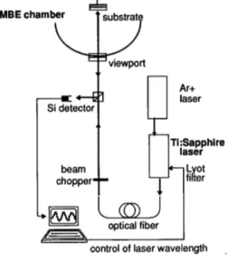
was measured with a pyrometer. To ensure temperature reproducibility, a systematic procedure was used, leading to oxide desorption at 610 °C. Moreover, the temperature range involved was observed to be very sensitive to the As contamination of the pyrometer viewport and care was taken to keep it clean throughout the study. Growth was performed at 600 °C for both III-V binaries. Growth rates, in the range of 1 µm/h, were adjusted by RHEED oscillations so as to optimize the growth of both binaries for the same As pressure. Temperature ramps were applied to III element cells to avoid flux transients at shutter openings. The experimental apparatus for in situ selective DOR measurements is shown in Fig. 1. External light source is provided by a titanium:sapphire cw tunable laser via an optical fiber. The laser beam illuminates the growing layer surface at an angle of 2° to the normal and is then reflected and detected by a Si photodiode. The resulting signal is demodulated by a lock-in amplifier and acquired as a function of time by a computer. Tuning of the wavelength within the range
investigated from 760 to 960 nm is achieved by means of a computer-controlled step-by-step motorization of the Lyot filter. This spectral range can be analyzed as a result of the use of two sets of laser mirrors.
Dynamic optical reflectometry consists of subjecting at nearly normal incidence a light beam on the surface of a growing sample.7 The reflected beam exhibits oscillations due to multiple reflection interferences as the
layer thickness increases. The oscillation period is equal to /2n, where n and are the real part of the layer refractive index and the incident beam wavelength, respectively. Assuming a constant growth rate G, the refractive index n of the growing material can easily be inferred from these reflectivity oscillations by using the following relation: n=/(2G), where is the oscillation period. Whatever the underlying multilayer structure this procedure can nonetheless be applied by taking care not to use the initial oscillation for this calculation, which is systematically shorter than the other oscillations due to phase shift. When the controlled layer is of the same type as the substrate, GaAs in our case, a decrease in contrast, or even cancellation of the oscillations can sometimes be observed. This phenomenon has already been described8 elsewhere and can be ac counted for by
a phase effect. This arises when the optical thickness of the already grown multilayer is about a multiple of /2, which makes the uppermost GaAs layer behave as if it were directly grown onto the GaAs substrate. In order to avoid this detrimental effect, a reflective multilayer, com- posed of some ~/4n-thick AlAs-GaAs alternating layers, was systematically grown prior to the GaAs period measurement. This procedure was found to greatly improve the oscillation contrast. However, GaAs measurement accuracy was observed not to be as good as for AlAs where absorption is not significant (see Fig. 3). First, index calibration was carried out. To do this, two samples were grown in the same run, under the same conditions of growth rate and temperature (600 °C). DOR was achieved at 0=920 nm on sample (a) using the aforementioned procedure. For ex situ calibration of the
growth rate by double crystal x-ray diffraction, sample (b) was used. It consisted of 16 periods of GaAs and AlAs alternating layers, with selected thicknesses of about a quarter-wave for 0. These GaAs and AlAs
thicknesses were measured to be 61.45 (±0.5) and 73.85 (±0.5) nm, respectively. These data were later confirmed by spectroscopic ellipsometry. GaAs and AlAs growth rates at 600 °C were then derived from these values measured at room temperature and from the thermal expansion coefficients of both semiconductors,14
and n(GaAs)=3.72. Given our experimental conditions (=±0.5 s, =±0.05 nm, thickness=±0.5 nm), the preceding values were determined within 0.8%. These index values, which correspond to 600 °C and 920 nm, were then used as a reference in the remaining part of the study.
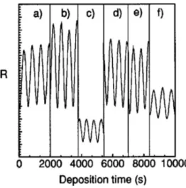
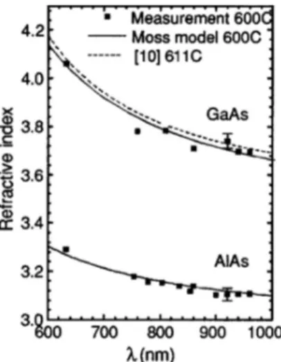
In a second step, index dispersion was determined. During the spectral study, attention was paid to maintaining the substrate temperature constant and equal to 600 °C. Reflectivity oscillation periods were measured at 920 nm, for reference, and at 760, 780, 810, 835, 860, 900, 940, and 960 nm (see an example given in Fig. 2). GaAs and AlAs refractive index variations were then inferred from their 920 nm reference value and from the experimental dispersion of the oscillation period. The results are shown in Fig. 3 for both materials. In addition, DOR measurements were performed by replacing the tunable laser with a He-Ne laser at =632.8 nm to provide comparison with the index values published and mainly measured at this wavelength. Our results were first compared in the case of GaAs with the HOA model dispersion at 611 °C.10 A good agreement was
obtained, as shown in Fig. 3, although the model yields slightly higher values than the experiment which can be accounted for by the temperature difference. The high temperature index dispersion was also calculated for both binaries from the Moss semi-empirical model,15 which relates index and band gap dependencies on temperature
according to the following relation
To do this, the index dispersion at room temperature n() was taken from Afromovitz’s model,16 while the
temperature variation of the band gap was derived from Varshni’s empirical relation17,18 and experimental
values18 for GaAs and AlAs, respectively. This leads to a dispersion law of the refractive index at 600 °C plotted
in Fig. 3 for both materials. Our experimental values turn out to be in good agreement with this law, which does not include any adjustable parameters. We now use this model for first-order modeling of multilayer optical behavior at high temperature.
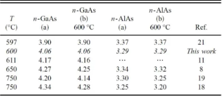
In order to compare our results with those published in the literature, mainly at 633 nm, the Moss model was also used to bring these values to 600 °C (see Table I). They were found to differ greatly. These discrepancies
could be accounted for by the difference in the models involved in the experimental techniques of characterization and by the lack of precision of the indicated temperatures. Indeed, achieving absolute calibration of surface temperatures in a reduced pressure (MOCVD) or high vacuum (MBE) environment is highly difficult. In our case, the values obtained for the GaAs and AlAs refractive indices within the wavelength range investigated will be used to control the growth of these semi- conductors at the temperature we consider to be 600 °C and calibrated by a systematic procedure.
To conclude, a new technique of in situ dynamic optical reflectometry taking advantage of a tunable laser light source has been presented. In a first step, this technique was successfully used to measure AlAs and GaAs refractive in-dices at a growth temperature between 760 and 960 nm, i.e., in a range in which they are seldom reported. These measured values were shown to be in good agreement with a model based on the Moss semi-empirical expression, which can then be used for the design of the optical behavior of III-V materials at growth temperature. This tunable DOR technique turns out to be highly flexible and particularly precise throughout this study. These advantages are now being used for precise real-time monitoring of the MBE growth of GaAs/AlAs Bragg reflectors and light modulators, as will be reported shortly.
Acknowledgements
The authors would like to thank Dr. A. Mun˜oz-Yagu¨e for fruitful discussions and Dr. G. Rolland and Dr. F. Bertin (LETI-CEA) for double-crystal x-ray diffraction and spectroscopic ellipsometry measurements.
References
1 P. L. Gourley and T. J. Drummond, Appl. Phys. Lett. 50, 1225 (1987). 2 K.-K. Law, J. L. Merz, and L. A. Coldren, J. Appl. Phys. 72, 855 (1992).
3 J. D. Walker, K. Malloy, and S. Wang, IEEE Photonics Technol. Lett. 2, 162 (1990). 4 S. A. Chalmers, K. P. Killeen, and E. D. Jones, Appl. Phys. Lett. 65, 4 (1994).
5 W. E. Quinn, D. E. Aspnes, M. J. S. P. Brasil, M. A. A. Pudensi, S. A. Schwarz, M. C. Tamargo, S. Gregory, and R. E.
6 H. Grothe and F. G. Boebel, J. Cryst. Growth 127, 1010 (1993).
7 J. V. Armstrong, T. Farrell, T. B. Joyce, P. Kightley, T. J. Bullough, and P.
J. Goodhew, J. Cryst. Growth 120, 84 (1992).
8 K. P. Killeen and W. G. Breiland, J. Electron. Mater. 23, 179 (1994).
9 W. G. Breiland and K. P. Killeen, Mater. Res. Soc. Symp. Proc. 324, 99 (1994).
10 P. Lautenschlager, M. Garriga, S. Logothetidis, and M. Cardona, Phys. Rev. B 35, 9174 (1987). 11 H. Yao, P. G. Snyder, and J. A. Woollam, J. Appl. Phys. 70, 3261 (1991).
12 C. H. Kuo, S. Anand, R. Droopad, K. Y. Choi, and G. N. Maracas, J. Vac. Sci. Technol. B 12, 1214 (1994). 13 E. Bedel, A. Mun˜oz-Yagu¨e, and C. Fontaine, Mater. Sci. Eng. 21, 157 (1993).
14 S. Adachi, J. Appl. Phys. 58, R1 (1985).
15 T. S. Moss, Optical Properties of Semiconductors (Butterworths, London, 1961). 16 M. A. Afromovitz, Solid State Commun. 15, 59 (1974).
17 Y. P. Varshni, Physica (Netherlands) 34, 149 (1969). 18 C. D. Thurmond, J. Electrochem. Soc. 122, 1080 (1988).
19 H. Sankur, W. Southwell, and R. Hall, J. Electron. Mater. 20, 1099 (1991). 20 N. C. Frateschi, S. G. Hummel, and P. D. Dapkus, Electron. Lett. 27, 155(1991). 21 T. Farrell, J. V. Armstrong, and P. Kightley, Appl. Phys. Lett. 59, 1203 (1991).
.
FIG. 2. AlAs reflectivity oscillation periods measured for several wave- lengths at T=600 °C: (a) 810 nm, (b) 860 nm, (c) 960 nm,(d) 780 nm, (e) 835 nm, (f) 920 nm.
FIG. 3. GaAs and AlAs refractive indices measured by DOR at T=600 °C. Dotted lines show the GaAs constants obtained by Yao et al. (Ref. 10) at 611 °C and straight lines the calculated dispersion law at 600 °C derived from the Moss odel.
TABLE I. GaAs and AlAs refractive indices at elevated temperature at 633 nm: (a) measured at different temperatures (b) brought to 600°C by Moss model.


