IR‐UWB AND OFDM‐UWB TRANSCEIVER NODES FOR
COMMUNICATION AND POSITIONING PURPOSES
MOHAMED ALJERJAWI
DÉPARTEMENT DE GÉNIE ÉLECTRIQUE
ÉCOLE POLYTECHNIQUE DE MONTRÉAL
THÈSE PRÉSENTÉE EN VUE DE L'OBTENTION
DU DIPLÔME DE PHILOSOPHIAE DOCTOR
(GÉNIE ÉLECTRIQUE)
DÉCEMBRE 2012
Cette thèse intitulée :
IR‐UWB AND OFDM‐UWB TRANSCEIVER NODES FOR
COMMUNICATION AND POSITIONING PURPOSES
présentée par :
en vue de l’obtention du diplôme de : ALJERJAWI Mohamed
a été dûment acceptée par le jury d’examen constitué de : Philosophiae Doctor M. CARDINAL Christian M. , Ph.D., président NERGUIZIAN Chahé M.
, Ph.D., membre et directeur de recherche BOSISIO Renato
M.
, M.SC.A., membre et codirecteur de recherche WU Ke
M.
, Ph.D., membre
To my beloved parents, sisters, wife and daughter For their endless love, encouragment and support
advice, guidance, and encouragement throughout my doctoral project and course work. I would also like to thank all thesis jury members for their time and remarks in reviewing this thesis.
My gratitude is also due to my colleagues: Tarek Djerafi, Ali Doghri, Lydia Chioukh, Farshad Sarabchi and Nguyen Van Hoang for their generous help.
I would like also to thank staff members and technicians of the Poly-Grames research center for their assistance and collaboration.
ses nombreux avantages tels que la faible probabilité d'interception et de la possibilité de combiner la communication des données de positionnement dans un seul système. Il existe plusieurs UWB couche physique (PHY) présentées initialement à la norme IEEE qui convergent en deux propositions principales: des porte-UWB ou Orthogonal Frequency-Division Multiplexing (OFDM-UWB), et à court d'impulsion porteuse à-UWB ou Impulse Radio-(IR-à-UWB). Une des plus grandes tâches difficiles pour les chercheurs est de nos jours la conception d'émetteurs-récepteurs UWB optimisés qui satisfont à des conditions rigoureuses, dont la simplicité caractéristiques large bande, à faible coût et de conception. Des études antérieures ont montré que les récepteurs à conversion directe basée sur Wave-radio interféromètre (WRI) circuits représentent un bon candidat pour les applications UWB. Circuits IRG ont plusieurs avantages tels que l'exploitation à large bande, à faible coût et la simplicité. Des travaux antérieurs sur l'IRG circuit, cependant, a enquêté sur le circuit de l'IRG sur la base du concept de porteuse unique signaux (par exemple, les signaux sinusoïdaux). L'objectif de ce projet est de fournir les résultats de conception, de simulation, de mise en œuvre et le test d'un émetteur-récepteur WRI basé sur ce que peut être utilisé comme un nœud ou un pico-réseau dans un détecteur sans fil / réseau de données. Nous allons passer par les étapes de conception et de mise en œuvre de propositions UWB deux: IR-UWB et OFDM-UWB. Pour la proposition porteuse à nous concentrer sur la conception et la mise en œuvre de l'émetteur-récepteur en intégrant les
dans cette thèse. La mise en œuvre de l'(IR-UWB) et (OFDM UWB-) émetteurs-récepteurs utilisant une nouvelle conception de Wave Radio-interféromètre (WRI) comme un circuit convertisseur abaisseur directement dans un canal réaliste UWB est présenté. Selon les spécifications IEEE 802.15.3a standard, un code MATLAB a été utilisé pour générer le modèle de canal pour des simulations et des mesures. Le même code représentant la réponse impulsionnelle du canal a été importé vers un émulateur de canal radio à imiter le comportement du canal sans fil pour les mesures en laboratoire. Une étude analytique de l'outil de taux d'erreur (BER) des deux émetteurs-récepteurs est prévu. En outre, pour les émetteurs-récepteurs proposés opérant dans la gamme de fréquences (3,1-4.1GHz), une étude comparative entre plusieurs modèles de canaux standard (CM1) et (CM4) est présentée pour chaque scénario. Le but de cette étude est de montrer meilleurs et les pires scénarios de rendement par rapport à des cas l'émetteur-récepteur proposée dans un canal réaliste décoloration aidé avec les résultats analytiques. En outre, différentes configurations de transmission / réception des antennes ont été envisagées, notamment à une seule entrée à sortie unique (SISO), une seule entrée multiple-sortie (SIMO) et à entrées multiples-sorties multiples (MIMO). Pour chaque
implémentations d'émetteur-récepteur les deux ont le même ordre de diversité. Toutefois, l'IR-UWB émetteur-récepteur présente une moyenne de 2 dB rapport signal sur bruit (SNR) de perte par rapport à la même configuration du nombre de transmettre et de recevoir des antennes UWB OFDM pour émetteur-récepteur. Cela est dû à la propagation par trajets multiples immunité héritée avantage dans les systèmes OFDM. En outre, les deux spectacles émetteurs-récepteurs sont analysés en considérant IQ dégradations de canal. Utilisation ± 0.5 dB et ± 9o que les déséquilibres d'amplitude et de phase, respectivement, il se trouve que OFDM UWB-récepteur est plus sensible aux erreurs de décodage en raison de la sensibilité élevée de sous-porteuses gigue de phase. En outre, les résultats obtenus démontrent que BER WRI-UWB émetteurs-récepteurs peuvent fournir des résultats comparables à la performance BER typiques émetteurs-récepteurs UWB. La formulation analytique fourni sert comme une limite supérieure sur la performance attendue de l'IRG BER-UWB systèmes. Plage de mesure a été limitée par la simulation et les outils de mesure. Une méthode de synchronisation filaire a été utilisé pour éviter l'expertise de synchronisation unique ne sont pas couverts dans cette thèse.
IEEE which converged into two main proposals: carrier‐based UWB or Orthogonal-Frequency Division Multiplexing (OFDM‐UWB), and short‐pulse carrierless‐UWB or Impulse-Radio (IR-UWB).
One of the biggest challenging tasks for researchers nowadays is the design of optimized UWB transceivers that would satisfy rigorous conditions, among which wideband characteristics, low-cost and design simplicity. Previous studies have shown that direct-conversion receivers based on Wave-Radio Interferometer (WRI) circuits represent a suitable candidate for UWB applications. WRI circuits have several advantages such as wideband operation, low cost, and simplicity. Previous works on WRI circuit, however, investigated the WRI circuit based on the concept of single-carrier signals (i.e., sinusoidal signals). The objective of this project is to provide the design, simulation, implementation and testing results of a WRI-based transceiver that can be utilized as a node or a piconet in a wireless sensor/data network. We will go through the design and implementation steps for both UWB proposals: IR-UWB and OFDM-UWB. For the carrierless proposal we will focus on designing and implementing the transceiver by integrating the transmitter/receiver operations in a single prototype, while for the carrier‐based proposal we will design and implement the transceiver with
in this thesis.
The implementation of the (IR-UWB) and (OFDM-UWB) transceivers employing a novel design of Wave-Radio Interferometer (WRI) circuit as a direct down-converter in a realistic UWB channel is presented. According to IEEE 802.15.3a standard specifications, a MATLAB code has been used to generate the channel model for simulations and measurements. The same code representing the channel impulse response has been imported to a radio channel emulator to imitate the wireless channel behavior for the laboratory measurements. An analytical investigation of the bit-error-rate (BER) performance of both transceivers is provided.
Also, for the proposed transceivers operating in the frequency range (3.1–4.1GHz), a comparative study between standard channel models (CM1) and (CM4) is presented for each scenario. The aim of this study is to show best vs. worst case performance scenarios for the proposed transceiver in a realistic fading channel aided with analytical results.
Further, different configurations of transmit/receive antennas have been considered including single-input single-output (SISO), single-input multiple-output (SIMO) and multiple-input multiple-output (MIMO). For each configuration, we provide the same comparative study for channel models CM1 and CM4. Simulation, analysis and measurement results demonstrate that both transceiver implementations have the same diversity order. However, IR-UWB transceiver shows an average 2dB signal-to-noise
susceptible to decoding errors due to subcarriers high sensitivity to phase jitter. Also, the obtained BER results demonstrate that WRI-UWB transceivers can provide comparable BER performance results to typical UWB transceivers. The analytical formulation provided serves as an upper bound on the expected BER performance of WRI-UWB systems. Measurement range was limited by simulation and measurement tools. A wired synchronization method was used to avoid unique synchronization expertise not covered in this thesis.
DEDICATION --- iii
ACKNOWLEDGEMENTS --- iv
Résumé --- v
Abstract --- viii
Table of contents --- xi
Figures List --- xiv
Tables List --- xviii
List of signs and abbreviations --- xix
CHAPTER 1 Introduction ... 1
1.1 Research overview --- 1
1.2 Research problem --- 3
1.3 Thesis objectives and contributions --- 3
1.4 Thesis outline --- 6
Chapter 2 UWB and WRI circuit background ... 7
2.1 Introduction --- 7
2.2 Review of ultra-wideband (UWB) technology --- 7
2.3 Review of Wave-Radio Interferometer technology --- 11
2.4 IEEE802.15.3a UWB channel model --- 15
2.5 Conclusion --- 19
CHAPTER 3 WRI Transceiver circuit ... 20
3.7 WRI Transceiver Design Features --- 39
3.8 S-Parameters Test Bench --- 41
3.9 Conclusion --- 46
Chapter 4 IR-UWB Tranceiver ... 47
4.1 Introduction --- 47
4.2 Methods of generating UWB waveforms --- 47
4.3 Pulse generation in the test bench --- 49
4.4 IR-UWB test bench implementation --- 52
4.5 Demodulation algorithm --- 57
4.6 Synchronization algorithm --- 61
4.7 BER performance analysis --- 63
4.8 Simulation and measurement results --- 65
4.8 Conclusion --- 75
Chapter 5 OFDM-UWB Transceiver ... 76
5.1 Introduction --- 76
5.2 Implementation challenges and limitations --- 77
5.3 OFDM-UWB test bench implementation --- 80
5.7 Conclusion --- 94
Chapter 6 Conclusions and future work ... 96
6.1 Conclusion --- 96
6.2 Future Work --- 98
proposal [19]. ... 10
Figure 2-3: Frequency bands, groups of frequencies, within each group of the MB-OFDM approach to UWB communications in 3.1- to 10.6-GHz unlicensed UWB bands proposed to the IEEE 802.15.3a WPAN standard [19]. ... 11
Figure 2-4: WRI reflectometer for microwave measurment. ... 12
Figure 2-5: WRI direct conversion receiver. ... 13
Figure 2-6: WRI Based SDR receiver architecture. ... 14
Figure 2-7: An IEEE 802.15.3a channel model realization. ... 18
Figure 3-1: WRI architecture using power combiners/dividers (PDC) and phase shifters (PS). ... 21
Figure 3-2: Typical test bench employing separate WRI circuits for the modulation and demodulation functions. ... 22
Figure 3-3: WRI with the same architecture used as a modulator (note the arrow directions compared to Figure 3-1). ... 23
Figure 3-4: WRI circuit model in Simulink. ... 25
Figure 3-5: Schematic of WRI circuit in ADS. ... 26
Figure 3-6: WRI normalized output voltages vs. phase difference between the input and reference signals at any frequency within the operating channel. ... 27
Figure 3-8: Error Vector Magnitude. ... 29
Figure 3-9: Combined effect of amplitude and phase imbalance. ... 30
Figure 3-10: Measured constellation of output modulated signal... 31
Figure 3-11: The core of the WRI transceiver. ... 34
Figure 3-12: Fabricated RF layer of the WRI transciever. ... 35
Figure 3-13: Fabricated DC layer of the WRI transceiver. ... 36
Figure 3-14: Optimized design for the Wilkinson PD/PC. ... 37
Figure 3-15: A picture showing both layers RF and DC of the WRI transceiver. ... 38
Figure 3-16: WRI transceiver S-parameters test setup. ... 42
Figure 3-17: Simulated vs. measured S11 of the WRI transceiver. ... 43
Figure 3-18: Simulated vs. measured S21 of the WRI transceiver. ... 44
Figure 3-19: Simulated vs. measured S21 phase response for the WRI transceiver for modulation states 1 and 3. ... 45
Figure 3-20: Simulated vs. measure S21 phase response for the WRI transceiver for modulation states 2 and 4. ... 45
Figure 4-1: A method of UWB pulse generation. ... 47
Figure 4-2: UWB pulse precision generation method. ... 48
Figure 4-3: Generated pulse train in the time domain [22]. ... 50
Figure 4-4: Generated pulse spectrum before upconversion [22]. ... 51
Figure 4-10: Illustration of demodulation algorithm for WRI circuit output ports. ... 57
Figure 4-11: FPGA implementation of demodulation algorithm. ... 60
Figure 4-12: Simulated output signals for three different delays. ... 61
Figure 4-13: Measured signals for three different delays. ... 63
Figure 4-14: An ideal log-detector model in Simulink. ... 66
Figure 4-15: Signals simulated at ports 3 to 6 of demodulator for modulation state 0. ... 66
Figure 4-16: Signals simulated at ports 3 to 6 of demodulator for modulation state 1. ... 67
Figure 4-17: Signals simulated at ports 3 to 6 of demodulator for modulation state 2. ... 67
Figure 4-18: Signals simulated at ports 3 to 6 of demodulator for modulation state 3. ... 68
Figure 4-19: BER theory, simulation and measurement curves comparison. ... 69
Figure 4-20: IR-UWB transceiver simulation, analysis and measurement results for CM1 and CM4. ... 70
Figure 4-21: SISO, SIMO (1x2) and MIMO (2x2) BER simulation and measurement results of IR-UWB transceiver for CM1. ... 72
Figure 4-22: SISO, SIMO (1x2) and MIMO (2x2) BER simulation and measurement results of IR-UWB transceiver for CM4. ... 72
Figure 4-24: Output measured and simulated signal constellations for different signal SNRs. ... 74 Figure 5-1: Block diagram of the OFDM-UWB test bench of the SISO transceiver. ... 82 Figure 5-2: Block diagram of the OFDM-UWB test bench of the SIMO (1x2)
transceiver. ... 83 Figure 5-3: Block diagram of the OFDM-UWB test bench of the MIMO (2x2)
transceiver. ... 83 Figure 5-4: OFDM-UWB transceiver simulation, analysis and measurement results for
CM1 and CM4. ... 89 Figure 5-5: SISO, SIMO (1x2) and MIMO (2x2) BER simulation and measurement
results of OFDM-UWB transceiver for CM1. ... 90 Figure 5-6: SISO, SIMO (1x2) and MIMO (2x2) BER simulation and measurement
results of OFDM-UWB transceiver for CM4. ... 90 Figure 5-7: SISO, SIMO (1x2) and MIMO (2x2) BER simulation and measurement
results of IR-UWB and OFDM-UWB transceivers for CM1. ... 91 Figure 5-8: SISO, SIMO (1x2) and MIMO (2x2) BER simulation and measurement
results of IR-UWB and OFDM-UWB transceivers for CM4. ... 92 Figure 5-9: SISO, SIMO (1x2) and MIMO (2x2) BER results of OFDM-UWB
transceiver for the ideal case and with amplitude and phase imbalances for CM1. ... 93
Table 5.1: Comparison between the parameters of the MB-OFDM and implemented OFDM-UWB systems. ... 79
CPW Co-planar waveguide
I In-phase
LUT Look-up-table
MHMIC Monolithic hybrid microwave integrated circuit
Q Quadrature
ADC Analog-to-digital converter
ADS Advanced Design System
AWGN Additive white Gaussian noise
BER Bit error rate
BPSK Binary phase shift keying
BPSM Binary phase spectrum modulation CRLH Composite right/left-handed
DAC Data access component
DSP Digital signal processing
DS-UWB Direct-Sequence UWB
DUT Device under test
EVM Error-vector-magnitude
FCC Federal Communications Commission FMCW Frequency modulation continuous wave FPGA Field programmable gate arrays
I-UWB Impulse UWB
LEs Logic elements
LO Local oscillator
MB-OFDM Multiband orthogonal frequency-division multiplexing
Mbps Mega bit per second
MB-UWB Multiband Ultra wide band MC-UWB Multicarrier Ultra wide band MIR Multi(six)-port impulse radio
MMIC Monolithic microwave integrated circuit M-PSK M-ary phase shift keying
Msps Mega symbol per second
NF Noise figure
PAM Pulse amplitude modulation PCS Personal communication system PPM Pulse position modulation PPM Pulse position modulation
QAM Quadrature amplitude modulation QPSK Quadrature phase shift keying
QPSM Quaternary phase spectrum modulation
RF Radio frequency
SDR Software defined radio
SIW Substrate integrated waveguide TFMA Time-frequency multiple access TSDF Timed synchronous data flow
U-NII Unlicensed National Information Infrastructure
UWB Ultra-wideband
WPAN Wireless personal area network WRI Wave-Radio Interferometer
communication systems capable of providing easier connectivity anywhere and anytime with high data transfer rates. On the other hand, wireless systems are now used for computer networking and internet access in addition to voice/video communications. Moreover, the emphasis has shifted from providing fixed voice services to general wireless digital services that allow a wide variety of applications [1]-[6]. As a consequence of this growth, the need to develop new higher-capacity and highly reliable communication systems is increasing and driving research work to develop more integrated services, providing higher data rates and more universal interface for a variety of applications.
Among the new emerging communication technologies, Ultra-wideband (UWB) technology has attracted interest from both researchers and the industry due to its numerous advantages such as low probability of interception and the possibility of combining data communication with positioning in a single system. Since applications targeted for UWB need to satisfy stringent design requirements, the goal of improving the inherent UWB transceivers design was the main focus of researches during the last few years [7].
applications. Those advantages include reducing circuit complexity and allowing a higher level of circuit integration than conventional heterodyne receivers [7]. Direct conversion receivers based on the Wave-Radio Interferometer (WRI) (commonly know in the literature by Multi-port circuits) have been proposed [8] as multimode or software receivers operating with digital signal processors (DSPs) programmed for a number of modulation schemes. The utilization of WRI circuit in homodyne receivers has been realized in several variants including mixers, modulators, demodulators and antennas [7].
Although previous research efforts tackled the implementation of homodyne transceivers for several technologies and frequency bands [9]-[12], none of these works considered testing these transceivers in realistic channel conditions. Also, those studies were limited in considering Impulse-Radio (IR) UWB standard only when homodyne transceivers were designed for communication and positioning application [13]. Moreover, as higher capacity and data throughput is nowadays a driving force for more research work, another deficiency found in previous works is the lack of considering multiple-transmit and receive antenna configurations. Taking into account all these factors, this thesis builds a frame work that considers implementing an UWB homodyne transceiver using IR and Orthogonal-Frequency Division-Multiplexing (OFDM) modulation schemes that can be applied in communication or positioning applications.
new modulation schemes like OFDM and multiple-antenna configurations on the transmitter and receiver sides.
In the present research project, the main goal is to develop a comparison and design efficient transceiver nodes using IR-UWB and OFDM-UWB standards. These transceiver nodes can be utilized for communications, tracking and positioning or short-range radar imaging. The most general objectives and specifications in a transceiver design for such applications are mainly controlled by parameters, such as cost, size, simplicity and power efficiency. To achieve these objectives, WRI circuit is used as an RF front-end for the transceivers. Furthermore, this study provides a realistic benchmark of both transceivers performance in UWB wireless channel. To achieve that, IEEE802.15.3a UWB standard channel is re-generated for simulation and emulation in the lab environment. Below, the main contributions in this thesis are addressed with emphasis on tackled challenges and their solutions.
1.3 Thesis objectives and contributions
The most important feature of a WRI circuit is the ability to perform accurate phase discrimination both in low radio frequency (RF) and millimeter wave frequency range. The phase discrimination capability is feasible over a wide bandwidth as long as the
implementation of wideband radio devices appears to be a unique challenge. Previous studies, investigating WRI circuit considering sinusoidal signals, have shown that WRI circuit has several advantages such as wideband operation, low cost, and simplicity. The entire 3.1–10.6-GHz UWB band can be covered with one or two WRI circuits fabricated with low cost integrated circuit chips. The WRI technology for UWB applications is therefore promising and this project will originally study this topic.
Consequently, the objectives of this research are as follows:
• As known, the use of WRI circuit as a digital modulator/demodulator was achieved previously by integrating ready system components to implement the WRI circuit. For the proposed carrierless UWB system, we introduce a design and implementation of a dual‐layer fully fabricated WRI circuit in the lab.
• Compared to the previous WRI circuit, the newly fabricated WRI circuit combines both functions of modulation and demodulation on the same circuit, which translates to lower cost and size.
• Another feature of the new WRI circuit is its dynamic range which extends to approximately double the dynamic range of the prior design due to the used of the log-power detectors.
• Implementation for an OFDM-UWB system in an emulated wireless channel with WRI circuit utilized for direct downconversion.
fading statistics between different channels.
• Providing analytical bit-error-rate (BER) expressions to benchmark IR-UWB
and OFDM-UWB transceivers performance.
In this project, a novel WRI circuit operating in the range (3.1-4.1 GHz) is designed, fabricated and utilized in test bench platforms considering IR-UWB and OFDM-UWB standards. Based on research work done previously on WRI technology [14], it can be concluded that the entire 3.1 GHz to 10.6 GHz UWB band can be covered with one or two integrated circuit chips. The testing platforms adopt quasi-symmetric receiver and transmitter architecture (using WRI circuits to digitally modulate and demodulate the input impulse phase spectrum in accordance with FCC UWB bandwidth). In the IR-UWB transceiver, digital baseband data is modulating the phase spectrum of the input pulse using the fabricated WRI circuit, while for OFDM-UWB it’s used to modulate the OFDM subcarriers. Then, modulated signals undergo an additive white Gaussian noise (AWGN) channel and a realistic channel fading based on IEEE802.15.3a standard using the channel emulator.
Some of the modulation and demodulation algorithms are developed in field- programmable gate array (FPGA) using digital signal processing (DSP) techniques.
1.4 Thesis outline
Based on this focus, this dissertation is arranged in six chapters. The current chapter presented the research overview, definition of the research problem, thesis objectives, and contributions. Chapter 2 will present the necessary background for UWB technology, WRI circuits and the IEEE802.15.3a UWB standard channel used to emulate the wireless channel behavior in the test bench. In Chapter 3, the newly fabricated WRI circuit is introduced where we show its S-parameters and phase response results. Chapter 4 covers detailed results of the IR-UWB transceiver utilizing the fabricated WRI circuit. Chapter 5 provides details on the OFDM-UWB transceiver results. Finally, conclusions and future works are summarized in Chapter 6.
efficient new wireless technologies and more optimized design for transceiver systems are pushing. In fact, some efficient promising wideband techniques like ultra-wideband (UWB) have been proposed, but the problem associated with them is how to provide efficient means of modulation and demodulation either on the baseband or the radio frequency domains. Besides that, a paramount challenge for UWB receiver systems is how to mitigate the wideband fading channel scenarios. In this chapter, a brief introduction of UWB technology considering its different modulation schemes IR and OFDM is introduced. Then, previous research accomplishments on WRI circuit are summarized with emphasis on different applications of the circuit. Finally, IEEE802.15.3a UWB channel model used in this work to emulate the wireless channel during simulation and lab measurements is presented.
2.2 Review of ultra-wideband (UWB) technology
Ultra-wideband (UWB) technology has attracted considerable attention in both short-range wireless communication and radio frequency (RF) location sensing applications. Major advantages of this technology include fine time resolution, resistance to multi-path, low probability of interception, potentially low complexity and low cost, and the possibility of combining data communication with positioning in a single system
[14]-bandwidth (
B
f ) greater than 0.20. The fractional bandwidth can be determined in (2.1) [19].2
H L f H Lf
f
B
f
f
−
=
+
(2.1) wheref
L is the lower frequency andf
H is the higher frequency -3dB points in the signal spectrum, respectively. Also, according to the Federal Communications Commission (FCC) report on UWB [20], a signal is recognized as UWB if the signal occupies 500MHz (or more) bandwidth at -10dB emission points regardless of the fractional bandwidth value. The radiation limit mandated by FCC for indoor UWB applications is maximum power output of -41.3dBm/MHz between 3.1GHz and 10.6GHz. Figure 2-1 shows the spectral mask mandated by the FCC for unlicensed UWB communications. Spectral mask of some existing radio standards, such as global positioning system (GPS) and personal communication system (PCS) are also shown in Figure 2-1 for comparison purposes.Figure 2-1: FCC spectral mask for unlicensed UWB communications and a comparison with other radio standards [21].
Current UWB systems can be primarily categorized into carrierless and carrier-based UWB. Carrierless UWB, also known as Impulse-Radio UWB (IR-UWB) utilizes very short pulse in transmission. Common choices of modulation scheme in IR-UWB communication include pulse position modulation (PPM), pulse amplitude modulation (PAM), and pulse shape modulation [22]. In above modulation methods, data information is conveyed either in position, amplitude or shape of a pulse. In this category, one of the leading proposals during UWB standardization activities is known as Direct-Sequence UWB (DS-UWB) [23]. In the DS-UWB system, as shown in Figure 1-2, the 3.1- to 10.6-GHz band is divided into a low band from 3.1 to 4.9 GHz and an optional high band from 6.2 to 9.7 GHz. The bandwidth of the high band is twice the bandwidth of the low band, resulting in shorter time-domain pulses in the high band. The 4.9- to 6.1-GHz band is purposely neglected to avoid interference with IEEE 802.11a devices operating in the 5-GHz unlicensed national information infrastructure (U-NII) bands. Each piconet of the DS-UWB operates in one of the two bands, and
piconets in the same band are separated by code-division multiplexing. The basic coverage cell, referred to as a picocell, has a nominal coverage range of about 10 m. A network operating within that range is referred to as a piconet.
Carrier-based UWB, however, uses multiple simultaneous carriers in transmission. Common forms of carrier-based UWB exist such as Multicarrier UWB (MC-UWB), Multiband UWB (MB-UWB). In this category, the leading proposal for the IEEE 802.15.3a is Multiband OFDM (MB-OFDM). The MB-OFDM system uses the OFDM technique in the UWB 3.1- to 10.6-GHz unlicensed bands. Following this approach, the spectrum is divided into 15 bands each of width 528 MHz. In each band, a 128-point OFDM system using QPSK modulation is implemented to limit the required precision of mathematical operations and make digital implementation at ultrahigh sampling rates feasible. Figure 2-3 gives an overview of the MB-OFDM proposal. The 15 bands in the
Figure 2-2: Frequency and time response of the two basic channels in the DS-UWB proposal [19].
3.1 − 10.6 GHz unlicensed UWB spectrum are divided into five groups of 528-MHz bands. Group 1 is the most desirable because group 2 interferes with U-NII bands and IEEE 802.11a devices, and higher groups have smaller coverage areas. Each physical
piconet is implemented in a band group and several logical piconets share a band group using different time-frequency multiple access (TFMA) codes.
Other research and development activities on UWB include UWB channel characteristics, UWB antennas, and generation of UWB waveforms, etc. More detail can be found in [8], [12] and [18].
2.3 Review of Wave-Radio Interferometer technology
The Wave-Radio Interferometer (WRI) was first used on microwave measurement to obtain the complex reflection coefficient of a device under test (DUT) [24]. The complex ratio of the device connected at one input ports of a WRI circuit can be determined by observing signal powers at the remaining four output ports which is called test ports. Figure 2-4 shows the diagram of a WRI circuit used for this kind of microwave measurement.
Figure 2-3: Frequency bands, groups of frequencies, within each group of the MB-OFDM approach to UWB communications in 3.1- to 10.6-GHz unlicensed UWB bands proposed to the IEEE 802.15.3a WPAN standard [19].
One of the benefits of WRI-based measurement technique is that these power observations at the test ports are from locations other than the position of interest. This feature can be utilized to avoid violating of uniformity using a uniform transmission line or waveguide at the interface between the WRI circuit and the DUT. Other methods of observing the signal (e.g.,via probes, etc.) at the position of interest also violates unfortunately the uniformity.
The concept of calculating the complex ratio of an incoming signal and a known local oscillator (LO) signal by using the WRI was then applied to communication receivers [12]–[16]. From a communication receiver point of view, the amplitude and phase information embedded in the complex ratio can be used for demodulating phase or amplitude modulated signals. In [12]–[16], the WRI technology was reported as a direct conversion receiver operated with sinusoidal signals at millimeter-wave and radio frequencies (RF). The WRI receivers, shown in Figure 2-5, directly demodulate the data information carried on a single carrier using quadrature-phase shift keying (QPSK), quadrature amplitude modulation (QAM), etc. Standard direct conversion usually uses
two quadrature (Q) carrier paths to do the direct conversion without intermediate frequencies (IF), i.e., the in-phase (I) and quadrature signal are separated at RF stage [25]. The previously reported WRI-based direct conversion receivers, however, use only one carrier and separates I and Q signals by signal processing after the four outputs at base band stage. This direct conversion or demodulation feature of a WRI circuit was applied to software defined radio (SDR) platform by utilizing the flexibility of signal processing at base band. As candidate SDR receiver architecture, the WRI-based configurable receiver architecture, shown in Figure 2-6, can demodulate several modulation schemes such as QPSK and QAM. Detail investigations of WRI SDR applications can be found in [16]-[18].
Besides the WRI based receivers, a direct quadrature phase shift keying modulator based on WRI technology was recently introduced for a single carrier signal [13]. The modulator is composed of a WRI circuit, a switch matrix and open and short terminations. A conventional QPSK modulator employs heterodyne architecture which requires two intermediate frequency (IF) mixers, in-phase and quadrature-phase carriers,
and an RF upconversion section. Compared with a heterodyne modulator, this direct QPSK modulator eliminates the need for IF modulation and RF upconversion, consequently reducing power consumption and circuit complexity. The WRI-based modulator, due to its lack of nonlinear elements, can be scaled dimensionally and operates from RF to millimeter wave frequency ranges, which is not the case with some other direct modulators [26], [27]. Also, extendibility to M-ary phase shift keying (M-PSK) is possible because the architecture allows a variety of terminations to be applied to its ports.
As an alternative to standard frequency modulation continuous wave (FMCW) radar sensor, the WRI-based radar was also investigated in [22]-[23]. Range information and Doppler frequency contained in the vector of complex ratio of the transmitted and received signal can be found using WRI phase/frequency discriminator.
Several fabrication technologies have been used for WRI circuits. The work in [16] demonstrated a WRI module fabricated using monolithic hybrid microwave integrated circuit (MHMIC). The MHMIC WRI module was used as a front-end for QPSK
Figure 2-6: WRI Based SDR receiver architecture.
W
R
and development of low-cost millimeter-wave integrated circuits by allowing the integration of planar and non-planar structures on the same planar platform [29]. Another example of WRI using integrated circuits operating at wide bandwidth between 0.9GHz to 5GHz is given in [19]. A recent study [30] showed a WRI circuit adopting a composite right/left-handed (CRLH) transmission line for its key components. A direct advantage is that dual bands 3.96GHz and 7.39GHz can be covered by the proposed WRI front-end.
The UWB WRI-based transceiver systems presented in this thesis provides comparative implementation studies of IR and OFDM modulations. Both implementations considers different configurations of transmit and receive antennas. Those implementations will also be tested in realistic fading environment by emulating IEEE802.15.3a channel model presented in the following section.
2.4 IEEE802.15.3a UWB channel model
The IEEE802.15.3a channel model was first introduced based upon the measurements in [31]. The statistical channel model was also provided in the same work. It has been adopted as a channel standard for wireless high speed data communications for UWB applications. One of the proposed physical-layer modulations, MB‐OFDM in [32],
environment only with a restriction of less than 10m between the transmitter and receiver, another comprehensive channel model was introduced [33]. This channel model, IEEE 802.15.4a has been primarily been considered for low data rate UWB applications (˂ 1Mbps), such as sensor networks. However, as indicated in [31], it is not restricted to these applications only, and can also be used for high speed UWB applications. The research work in [34] provides a great reference for comparison between these models. In the following, we will present the statistical modeling of the IEEE 802.15.3a standard channel model [35], which is used to generate the channel impulse response employed in the simulations and the test bench.
The channel impulse response can be represented by
ℎ𝑖(𝑡) = 𝑋𝑖∑𝐿𝑙=0 ∑𝐾𝑘=0 𝛼 𝑘,𝑙𝑖 𝛿�𝑡 − 𝑇 𝑙𝑖 − 𝜏 𝑘,𝑙𝑖 � (2.2)
where i l k,
α is the multipath gain coefficient, with i referring to the impulse response
realization, l to the cluster number, and k to the arrival within the cluster. Tlirepresents the delay of the lth cluster for the ith channel realization, while i
l k,
τ is the delay of the kth
multipath component relative to the lth cluster arrival time for the same channel
realization. The large-scale shadowing statistics for the ith channel realization are represented by log‐normal distribution, represented by Xi in equation (2.2). After
where Λis the cluster arrival rate, and λ is the ray arrival rate, i.e., the arrival rate of a
path within each cluster. The behaviour of the (averaged) power delay profile is [35]
− Γ Γ − Ω = Ε γ τ α l k l e e i l k , 0 2 , (2.5)
which reflects the exponential decay of each cluster, as well as the decay of the total cluster power with delay.
In order to use the model, several of the above parameters need to be defined, which helps relate the model to actual measurements. Table II in [32] provides some target parameters for various line‐of‐sight and non-line‐of‐sight (NLOS) channels. The parameters of the model were found through an extensive search, which attempted to match the important characteristics of the statistical channel model output to the characteristics of actual measurements. The important channel characteristics include the mean excess delay, the root-mean square (RMS) delay spread, the mean number of paths within 10 dB of the peak, and the mean number of paths, which capture 85% of the channel energy. A channel realization generated for this model is shown in Figure 2-7.
Figure 2-7: An IEEE 802.15.3a channel model realization.
There are four main IEEE MB-OFDM UWB channel models proposed by the IEEE 802.15.3a Task Group, accounting for the four typical multipath scenarios of UWB systems. Namely CM1 with a line-of-sight (LOS) scenario with a distance between the transmitter and receiver reaching up to 4 m; CM2 non-line-of-sight (NLOS), with a separation from 0 to 4m, CM3 non-line-of-sight (NLOS), with a separation from 4 to 10m, and CM4 proposed to fit the channel with a rms delay spread of 25ns representing an extreme NLOS multipath channel. In this thesis and in the following chapters, we consider the CM1 and CM4 for system performance analysis between best vs. worst case scenarios.
Take note that in order to test both UWB transceiver implementations; an emulated channel is used in both simulation and measurement results. Those obtained results are based on simulating IEEE 802.15.3a channel model and not a real-time wireless channel.
requirements and the definition of UWB technology. Then, the OFDM technique was briefly highlighted upon for its importance and hence practicality for the use in wireless systems. In addition, previous research accomplishments on WRI circuit are summarized with emphasis on different applications of the circuit. Finally, IEEE802.15.3a UWB channel model used in this work to emulate the wireless channel during simulation and lab measurements is presented.
3.1 Introduction
The development of the proposed IR-UWB and OFDM-UWB transceivers mandated the design and fabrication of an RF front-end which satisfy low-cost, high-performance and versatility requirements. This chapter presents the design and implementation of a new transceiver based on the WRI circuit topology. This transceiver has the advantage of combining both functions of transmission and reception for an impulse UWB signal over the design frequency range (3.1‐4.1 GHz). In order to clarify the concept principle, a brief description of the WRI operation as a single operation circuit, (i.e., a modulator in the transmitter side and a demodulator in the receiver side) will be provided, then the circuit design, challenges and implementation steps carried for the new WRI transceiver will be presented.
3.2 Modulator WRI
A review of traditional implementations of the WRI is presented in [16]. The proposed transceiver in this work adopts the new WRI architecture introduced in [17], whose block diagram is shown in Figure 3-1. It is composed solely of power dividers/combiners (PDC) and phase shifters (PS), whereas earlier architectures required hybrid couplers in addition. A typical test bench utilizing WRI circuit for the transmitter and the receiver is shown in Figure 3-2. The transmitter in the test bench shown in Figure 3-2 consists of a wave‐radio circuit, a switching matrix and open/short circuit terminations. The modulator WRI shown operates as follows. Port 1 is fed with a
signal which acquires different phase states depending on the terminations applied at ports 3 to 6.
Figure 3-1: WRI architecture using power combiners/dividers (PDC) and phase shifters (PS).
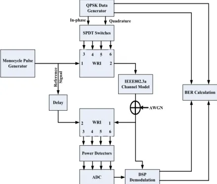
Monocycle Pulse Generator WRI SPDT Switches IEEE802.3a Channel Model WRI Power Detectors ADC DemodulationDSP BER Calculation Reference Signal In-phase Quadrature 1 2 2 1 3 4 5 6 3 4 5 6 Delay AWGN
Figure 3-2: Typical test bench employing separate WRI circuits for the modulation and demodulation functions.
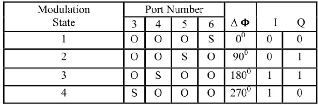
Table 3.1: Open and short circuit terminations criteria for the four QPSK modulation states.
Modulation
State 3 Port Number 4 5 6 ∆ 𝚽 I Q
1 O O O S 00 0 0
2 O O S O 900 0 1
3 O S O O 1800 1 1
4 S O O O 2700 1 0
3.3 Demodulator WRI
The receiver in the test bench shown in Figure 3-2 is composed of the same wave‐radio circuit structure, with the exception that inputs and outputs are acquired from
power available at ports 3 to 6. Then with the aid of proper digital signal processing algorithms, demapping of the transmitted symbol can be achieved efficiently.
Figure 3-3: WRI with the same architecture used as a modulator (note the arrow directions compared to Figure 3-1).
3.4 Simulation of WRI
As shown in [36], the transfer function between port 1 and port 2 of the WRI circuit can be derived and expressed as follows:
𝐻 = 0.707 × 𝑒−𝑗(4𝜑+ 2𝜃+𝑖.900), 𝑖 = 0, 1, 2, 3 (3.1)
where 𝜑 is the phase change of the power divider/combiner branch, 𝜃 is the phase change of the transmission line, i represents the ith configuration of four different
and the transmission lines. It can be designed to be discrete multiple of 360º in order to eliminate the phase variation of the modulated signal.
An ideal WRI circuit simulation model was first developed in the environment of Matlab-Simulink [37]-[39]. According to the S-parameters of the components used in the WRI circuit, the mathematical relationships between two inputs and four outputs of the WRI circuit are depicted using the Simulink model editor. The model simulating an ideal WRI circuit is shown in Figure 3-4.
Using the complex numbers for the above model is straightforward because an S-parameter at a frequency point is a vector including both amplitude and phase. The model eliminates the frequency variable. Thus it is a frequency-independent model. This infers that the phasor representation of a signal must be used to implement a system simulation based on this model. For an M-ary phase shift keying signal, its phasor representation can be written using Euler’s theorem as follows [40]:
𝑠(𝑡) = Re ��2𝐸𝑇� 𝑒𝑗𝜔0𝑡𝑒𝑗∅𝑖𝑡, 0≤ 𝑡 ≤T,
𝑖 = 1, … , 𝑀 (3. Error! Bookmark not de�ined.) where the phase term,
φ
i( )
t
, will haveM
discrete values, typically given by:∅𝑖(𝑡) =2𝜋𝑀 , 𝑖 = 1, … , 𝑀 (3.2)
The parameter
E
represents the symbol energy,T
the time duration and 𝜔0 the carrierusing the WRI circuit model given in Figure 3-4.
(ADS) software. In the simulation, a WRI circuit model was implemented based on the structure shown in Figure 3-1. The schematic of the modulator simulation is shown in Figure 3-5. The power divider/combiner was simulated using ideal S-parameters. Under different termination configurations, the output waveforms of the various QPSK modulation states were obtained and are shown in Figure 3-6. They agree with the results derived from (3.1).
Figure 3-6: WRI normalized output voltages vs. phase difference between the input and reference signals at any frequency within the operating channel.
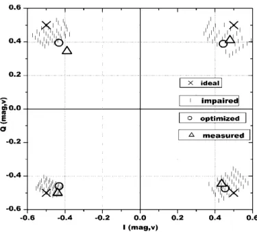
A more realistic simulation was performed using the measured S-parameters of the fabricated WRI in order to study the effect of phase and amplitude imbalances. The simulated WRI used in the test bench set up has a maximum amplitude imbalance of ±0.3 dB and phase imbalance of ±3 degrees.
An IQ impairment analysis is done by sweeping the amplitude imbalance between -0.3 dB to -0.3 dB and the phase imbalance between -3º to 3º. The simulation results show that the phase difference ranges from -11.3º to 11.4º and the amplitude difference ranges from 0.3dB to 2.3dB. The impaired I-Q constellation points are presented in Figure 3-7 and compared with the ideal points.
Figure 3-7: Comparison of I-Q constellations obtained by varying phase and amplitude.
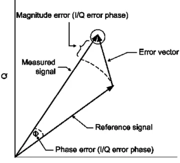
An error vector analysis is further done to quantify WRI circuit performance in terms of magnitude and phase errors. The figure of merit, Error-Vector-Magnitude (EVM), is the unsigned scalar distance between the end points of reference phasor and actual or measured phasor [41]. EVM is defined in (3.4) as a percentage of the peak signal level, usually defined by the constellation’s corner stage (Figure 3-8).
100%
average error magnitude
Error vector magnitude
peak signal magnitude
than a 2º phase difference from the ideal case. The EVM is as low as 14.5% which indicates that this modulator can achieve acceptable phase modulation accuracy. Note that the contribution to EVM by the phase and amplitude imbalance can be reduced by optimal design method described in the following text.
Figure 3-8: Error Vector Magnitude.
effective for analyzing or troubleshooting the effect of phase and amplitude imbalance existing in a WRI modulator.
To overcome the I-Q impairment, an optimization process was designed according to (3.1). Lengths of transmission line connecting cables are specified as parameters to be optimized under the goal of minimizing both the phase and amplitude errors. During the optimization process two different search methods, gradient and random, were used for better accuracy. The WRI circuit design was modified using the optimal lengths and simulated again. The optimized I-Q constellation is compared with ideal and impaired points in Figure 3-7. Note that the contribution to the I-Q impairment by the phase and amplitude imbalance can also be reduced by calibration algorithms used in receiver processing [42].
In order to verify the amplitude and phase balance of the optimized WRI circuit, S-Figure 3-9: Combined effect of amplitude and phase imbalance.
an amplitude difference from 0.5 dB to 2.7 dB were achieved, which shows close correlation with the previous optimized result.
The WRI circuit was further measured with commercial microwave switches and a digital data generator. The data generator provides two rectangular pseudo random sequences. One sequence is for in-phase (I) channel and the other is for quadrature (Q) channel. These modulating sequences were used to switch opens and shorts onto ports 3-6. Each sequence is at a symbol rate of 10 Msps. Thus a data rate of 20 Mbps was
measured and shown in Figure 3-10. During this measurement campaign, the carrier signal had a frequency of 3.6 GHz and 12 dB signal-to-noise (SNR) ratio.
3.5 Transceiver WRI
In previous works, the WRI was employed as one of two variants. At the transmitter side, it was used only as a modulator, while at the receiver side it was used only as a demodulator. In order to cope with the requirements of current and future wireless technologies employed either for localization or communication purposes, we initiate here the idea of not only integrating on the same board but also merging within the same WRI the transmitter and receiver operations.
Based on the operation requirements of the wave‐radio interferometer as a modulator/demodulator in the transmitter/receiver, the design of the WRI transceiver can be obtained as follows.
First, in order to operate as a modulator while in the transmission mode, we must apply to ports 3 to 6 short circuit (S) or open circuit (O) terminations according to the criteria defined in Table 2.1. Secondly, in the receiver mode, and to operate as a demodulator, a power detector is required also at ports 3 to 6. These two configurations may be accommodated by the use of a single‐pole triple‐throw (SP3T) switch at each of these ports. However, due to some practical aspects, such as switching speed, isolation between the switched ports and required Transistor‐Transistor Logic (TTL) switching control voltages, the choice settled on using a single‐pole quad-throw (SP4T) switch
RF3 and RF4 are the transmitter ports, which are respectively connected to a short and open circuits provided by open‐ended transmission lines, where the short circuit is achieved by an extra quarter‐wavelength section.
Previous implementations of the WRI demodulator used Schottky diodes for power detection. While these diodes are well known for their fast switching speeds and low forward voltage dropping, yet they suffer from low dynamic range capabilities. We have therefore selected a logarithmic‐detector (Analog Devices AD8317), which is capable of accurately converting an RF input signal amplitude (i.e. power) to a corresponding decibel‐scaled output voltage. This detector can be seen in Figure 3-11 at RF2 of the SP4T switch.
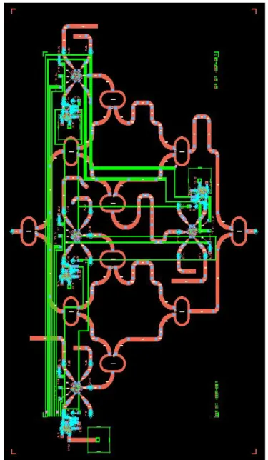
The implementation of the WRI transceiver required the design and fabrication of two substrate layers, one for RF and another one for DC. The layout of the RF layer, which is essentially constituted of the wave‐radio circuit with the SP4T switch circuit shown in Figure 3-11 at ports 3 to 6, is shown in Figure 3-12. This layer was designed considering a central carrier frequency of 3.6 GHz. As mentioned earlier, to provide more design flexibility by controlling these switches using the FPGA board, Hittite’s SP4T switch has been used since its controls (CTLA and CTLB in Figure 3-11) operates
with relative permittivity (εr = 2.33), thickness of 31mils and a loss tangent of 0.0012.
This substrate was chosen to allow large separation between transmission lines on the RF layer to avoid any cross coupling effects.
Figure 3-12: Fabricated RF layer of the WRI transciever.
In order to test the dynamic range capability of the log-detector in the lab, an experimental testing was conducted were the input signal power was varied and the corresponding output signal value is measured. The AD8317 log‐detector tested in the lab provided a dynamic range extending from ‐55 dBm to +5 dBm, corresponding approximately to the double of the dynamic range offered by a Schottky power detector. These two surface‐mount chips have been also used for their wideband characteristics, which is mandatory for UWB based applications. The layout of the DC layer, which is connected to the RF layout using vias, is given in Figure 3-13. This layer provides the interface to the FPGA board for control purposes. Further details about the design, fabrication and testing of the WRI transceiver can be found in [43].
Figure 3-13: Fabricated DC layer of the WRI transceiver.
3.6 Design and fabrication challenges
The initial stage of the design of the RF layer was based upon the optimization of the Wilkinson power divider/combiner design. The first implementation of the Wilkinson power divider/combiner suffered from cross coupling between the two λ/4 sections of the Wilkinson PD/PC and the following branches of transmission lines. Hence, by redesigning and testing a new layout of the Wilkinson, after adding extra spacing between the λ/4 sections and the following transmission lines, the cross-coupling problem was eliminated. The final design for the optimized Wilkinson is shown in Figure 3-14.
Figure 3-14: Optimized design for the Wilkinson PD/PC.
The second encountered challenge was the proper length choice of the extension transmission lines connecting ports 3, 4, 5 and 6 to their corresponding SP4T switches. Since the basic operation of providing a certain phase shift for the output pulse rely basically on the vector addition/subtraction of the signals reflected from these ports, these lengths have been carefully chosen in order to provide the same phase drift between the common port of the Wilkinson PD/PC and port RFC of the SP4T switch in Figure 3-11.
The third challenge was finding the best compromise between reducing the size of the RF layout of the designed prototype, and choosing the proper distance between the 90o,
180o phase shift extra length transmission lines and the surrounding components on the
layout in order to avoid any cross coupling that might occur.
The fourth challenge was properly designing and aligning both the RF and DC layers, and choosing the proper locations for the VIAs that connect both layers so that puncturing wouldn’t cause any malfunction in the required operation of any layer.
modulator and demodulator in the same prototype. This in consequence translates into smaller size and lower cost prototype.
2. The new design of the WRI transceiver is based upon the design and fabrication of both RF and DC layers in the lab, while the one in [40] relies totally on ready system components.
3. As a demodulator, the design in [40] utilized Schottky diodes as power detectors. However, the newly designed WRI transceiver employs log-detectors for this purpose. As mentioned earlier, these detectors are well recognized for their wide dynamic range which is almost double the one provided by Schottky diodes. This is mandatory; especially for systems destined to work in UWB standards were signal emissions have very low power levels.
4. Isolation between the transmitter and receiver is inherent by the isolation capabilities of the SP4T switch. This is due to the fact that both functionalities are obtained using the same circuit structure. Therefore, the expected isolation between the transmitter and receiver in this scenario can be measured by the achieved isolation between the switch common port and its output ports. As shown in Figure 3-16, a minimal isolation value of 27dB is measured along the
Figure 3-16: Measured isolation result between the common port of the SP4T switch and output port 2.
Since that the whole process of designing and fabricating the WRI transceiver was performed in the lab, redesigning a compact version of the transceiver can be achieved by changing the fabrication technology, such as MHMIC or MMIC fabrication technologies.
EP1S80B956C6 Altera FPGA board controls the SP4T switches based on the input in‐phase (I) and quadrature (Q) components of the original data stream. Corresponding to the criteria defined in Table 3.1, a very high speed integrated circuit hardware description language (VHDL) program configures the FGPA board, changing the switch positions between RF ports 3 or 4 on each of the WRI ports 3 to 6 according to the desired modulation state at the output. The Agilent 33250A Waveform Generator is used as a 20 MHz clock generator for the FPGA board. The S‐parameters of the WRI transceiver are measured by the Anritsu 37369D Vector Network Analyzer (VNA).
Figure 3-17: WRI transceiver S-parameters test setup.
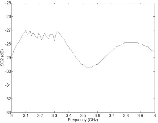
Using the pre‐described test setup, the following S‐parameter results for the WRI transceiver were obtained. Figure 3-18 shows the input reflection coefficient (S11) for the
transceiver. Along the entire bandwidth of 3.1 to 4.1 GHz, the transceiver maintains an S11 below ‐15 dB. Moreover, the minimum return loss is obtained approximately at the
design frequency (3.6 GHz). The forward transmission coefficient (S21) for the WRI
transceiver is shown in Figure 3-19. In this figure we can see clearly S21 confined within
the range of ‐4 to ‐9 dB throughout the 3 to 4 GHz bandwidth spectrum. This loss is incurred as a result of the use of the Wilkinson power divider, in addition to the loss caused by the SP4T switches at ports 3 to 6 of the transceiver. As shown in [40], a
small deviation between simulation and measurement may be due errors in the VNA calibration.
Figure 3-19: Simulated vs. measured S21 of the WRI transceiver.
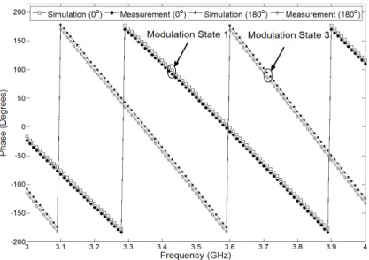
Figure 3-20 and Figure 3-21 show the phase response for the forward transmission coefficient (S21) of the WRI transceiver. In Figure 3-20, it is observed that for the
modulation states 1 and 3, at the design frequency of 3.6 GHz, the expected phase shifts of 0o, and 180o, respectively, can be obtained. Moreover, Figure 3-21 shows that at the
same frequency, the expected phase shifts of 90o and 270o are obtained for the modulation states 2 and 4, respectively. These two figures also exhibit close agreement between measured and simulation results, with a small discrepancy not exceeding 9o. The phase difference between the simulation and measurement curves can be returned to the inaccuracies during the layout fabrication process. This small phase drift is not expected to affect the detector decision except for small signal-to-noise ratios (SNRs) when the location of the received symbols is very close to the decision regions
Figure 3-20: Simulated vs. measured S21 phase response for the WRI transceiver for
modulation states 1 and 3.
Figure 3-21: Simulated vs. measure S21 phase response for the WRI transceiver for
demodulator was discussed. Also, a newly designed and fabricated dual-layer WRI transceiver circuit has been introduced. Then, design steps, fabrication challenges and features were presented. In order to enhance circuit characteristics, an optimization process was adopted. Following this optimization process, a test bench to verify the S-parameters of the fabricated circuit was developed. The obtained results demonstrate that the fabricated circuit has an acceptable return loss and linear phase response along the design frequency range of 3.1 - 4.1 GHz. This fabricated circuit constitutes the main component that will be used to build up both standard UWB transceiver nodes as will be discussed in the next two chapters.
waves to transmit the information. This pulse directly generates a very wide instantaneous bandwidth signal with a very low duty cycle. Since this UWB approach covers a wide spectrum of applications, it has been under great interest of development from researchers [43, 44].
Building upon aforementioned advantages of WRI circuit, in this chapter, using the fabricated WRI circuit in Chapter 3, we present the IR-UWB transceiver development steps including signal generation, test-bed implementation procedure and obtained simulation and measurement results.
4.2 Methods of generating UWB waveforms
One way of generating UWB signals is to use very sharp signal transitions in time followed by a band-pass filter (Figure 4-1) [45]. Sharp signals can be a step function or narrow rectangular pulse. Sharp signal transitions and extremely narrow pulses act like extremely wideband energy sources, which are then shaped by the desired band-pass filter. This method is a simple and effective method of generating UWB signals. It is
UWB signals can also be generated using precision signal design method. Figure 4-2 shows an example of this method. In this approach, we can synthesize UWB signals with precision in both the signal shape and its placement in the frequency spectrum. To that end, signals can be shaped at base band and then shifted in frequency to the desired location in the spectrum using heterodyning technique. Band shaping is much easier to accomplish at base band than at higher radio frequencies.
Another approach to generate UWB signals is Fourier Series-Based pulses generation [46]. In this approach, an UWB signal is generated in the frequency domain by summing harmonics of the desired signal instead of generating the signal by a single high-power in the time domain. The Fourier series is normally used to decompose periodic signals into sinusoids as described in (4.1).
expansion of the pulse train to be produced and then generating and transmitting each sinusoidal component of the expansion. A separate oscillator produces each harmonic component of Fourier series expansion and the sum of all the oscillators will reproduce the desired periodic pulses. Only finite terms of Fourier series can be used because of finite number of oscillators. The DC component should not be included in the waveform generation because an antenna cannot transmit the DC component. With these constraints, we can synthesize a desired pulse train from the truncated Fourier series expansion approximately.
For other UWB proposals, such as multi-band orthogonal frequency-division multiplexing (MB-OFDM), instead of using impulse principle, the MB-OFDM UWB signals consists of the parallel transmission of several signals that are modulated at different carrier frequencies occupying the correct spectrum allocation.
4.3 Pulse generation in the test bench
In the experiment of the proposed platform, the precision signal design method was adopted to generate the impulse UWB signal. The pulse signal in the chosen channel (3– 4 GHz) is generated using a rectangular pulse generator, a low pass filter, an upconverter, and a band pass filter shown in Figure 4-2. The pulse generator generates a
respectively. A low pass filter with 500 MHz cut-off frequency is used to filter out frequency points beyond 500 MHz of the rectangular pulse spectrum. The upconverter operates at a center frequency of 3.5 GHz and it converts the portion of the rectangular pulse signal spectrum to a signal spectrum occupying 1-GHz bandwidth between 3–4 GHz. Figure 4-5 shows the spectrum of the generated UWB signal.
Figure 4-5: Generated pulse spectrum after upconversion [22]. Figure 4-4: Generated pulse spectrum before upconversion [22].
During this study, the WRI BER was the primary parameter of concern. The test bench used for the BER measurement in the lab is shown in Figure 4-6. The pattern pulse generator Anritsu ME522A transmitter was used to provide the input for both WRI transceivers shown in the figure. In fact, the input signal will act as the required input pulse for the WRI transceiver when it is in its transmission mode, while it will represent the reference signal for the other WRI transceiver which will be operating in its receiving mode. The input pulse duration was adjusted to 10 nsec, with a maximum pulse repetition frequency of 20 MHz. To control both WRI transceivers, the following modifications have been made to the VHDL program.
Monocycle Pulse Generator WRI QPSK Data Generator SPDT Switches IEEE802.3a Channel Model WRI Power Detectors ADC DemodulationDSP BER Calculation Reference Signal In-phase Quadrature 1 2 2 1 3 4 5 6 3 4 5 6 Delay AWGN
Figure 4-6: IR-UWB SISO test bench employing WRI circuits for the modulation and demodulation functions.
the WRI transceiver is operating as a receiver, the FPGA board will trigger the SP4T switch position to RF port 2, and will activate the Log-Detector through its VPOS TTL activation VIA (Figure 3-11).
As previously mentioned, in order to define the modulation state, we need to determine which Log-Detector has a minimum at its output port for every pair of the I and Q data streams. Hence, the output ports of the Log-Detector for the WRI transceiver operating in its receiving mode are connected to Analog Devices AD8564 Comparator. This comparator will provide a TTL output that can be fed to the FPGA board, which will help to determine the minimum port, (i.e. modulation state), and regenerate the I and Q data streams for BER measurement purposes. Furthermore, using the modified VHDL program, the FPGA board was configured to transform the regenerated I and Q streams into a single output stream which was compared to a synchronized replica of the transmitted stream using Anritsu ME522A receiver equipment. Figure 4-7 shows the test setup used for BER measurements of the WRI transceiver.
Figure 4-7: IR-UWB transceiver test setup.
The UWB wireless channel based on IEEE802.15.3a standard is resembled in the test bench by EB Propsim C8 Channel Emulator. The generated channel model using MATLAB is exported to the emulator, with the input of one of its RF interfaces connected to port 2 (output) of the transmitter WRI, while the output of the interface has been connected to port 1 (input) of the receiver WRI. The 100MHz RF bandwidth limitation of the emulator dictated a maximum pulse bandwidth of 100MHz. This pulse has been upconverted using 5 of Hittite’s (HMC170C8) surface mount mixers with LO frequencies of 3.15, 3.25, 3.35, 3.45 and 3.55GHz generated using Wiltron synthesized sweep generator. Hence, a signal with a total bandwidth of 500MHz has been created and transmitted over the wireless channel.
We have also considered in this study the implementation of multiple transmit/receive antenna configurations of the same transceiver. The reason being is to
It has been reported that for multiband UWB systems, adding more antennas in the transmitter, receiver or both sides simultaneously will generally enhance the coverage range, data rate and BER [47].
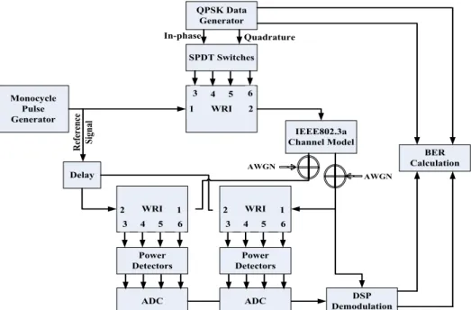
The SIMO and MIMO implementations of the IR-UWB transceiver are shown in Figure 4-8 and Figure 4-9, respectively. For those implementations, two WRI circuits are used in the receiver with joint combining using DSP demodulation. Synchronization is maintained between the transmitter, channel emulator and the receiver using the reference signal.
Monocycle Pulse Generator WRI IEEE802.3a Channel Model WRI Power Detectors ADC DemodulationDSP BER Calculation Reference Signal 1 2 2 1 3 4 5 6 3 4 5 6 Delay WRI Power Detectors ADC 2 1 3 4 5 6 AWGN AWGN
Figure 4-8: Block diagram of the IR-UWB test bench of the SIMO (1x2) transceiver.
design-ready intellectual property (IP) functions provided with the DSP platform significantly shortens the implementation time. Figure 4-10 illustrates the basic functions of the demodulation algorithm for the modulated signal.
Figure 4-10: Illustration of demodulation algorithm for WRI circuit output ports.
Four output signals are sampled by analog-to-digital converters. Then samples are integrated over the pulse repetition period (T ). At the clock times of t kT= , a
comparison of accumulator output is done and the port with minimum amplitude is determined. If the amplitude of s3 is minimum, symbol (0) is given. And the rest symbol (1, 2, and 3) can be deduced by analogy. Symbol (1) is corresponding to the minimum amplitude present at port 4. Symbol (2) is corresponding to the minimum
![Figure 2-1: FCC spectral mask for unlicensed UWB communications and a comparison with other radio standards [21]](https://thumb-eu.123doks.com/thumbv2/123doknet/2322822.29479/30.918.255.729.177.402/figure-fcc-spectral-unlicensed-communications-comparison-radio-standards.webp)
![Figure 2-2: Frequency and time response of the two basic channels in the DS- DS-UWB proposal [19]](https://thumb-eu.123doks.com/thumbv2/123doknet/2322822.29479/31.918.189.739.191.495/figure-frequency-time-response-basic-channels-uwb-proposal.webp)