I | P a g e
UNIVERSITÉ DU QUÉBEC
INSTITUT NATIONAL DE LA RECHERCHE SCIENTIFIQUE
ÉNERGIE MATÉRIAUX TÉLÉCOMMUNICATION
RECONFIGURABLE PERIODIC STRUCTURES FOR BEAM STEERING
APPLICATIONS
By
Reza Amiri
A dissertation submitted in partial fulfillment of the requirements for the degree of
Master of Science (MSc.) in Telecommunications
Evaluation Jury
Research Director Prof. Douglas O'Shaughnessy, [INRS-EMT]
Internal Examiner Prof. Mourad NEDIL, [Université du Québec]
External Examiner Prof. Ahmed KISHK, [Concordia University]
II | P a g e
A
CKNOWLEDGMENTPrimarily, I would like to convey my most genuine gratitude and appreciation for my adviser Professor Tayeb Denidni for the incessant encouragement, assistance, and support in regards to my Master study and the research conducted, for his enduring patience, infinite motivation, for the work I was doing, as well as his immeasurable knowledge. It was his aspiring guidance, invaluable constructive criticism and friendly advice that has helped me in the dimmest and most pessimistic times of conducting my research and writing this thesis, and I could not have envisioned having a finer mentor.
My most heartfelt appreciation also goes to my fellow group members: Javad Pourahmadazar, Dr. Behnam Zarghooni, Arun Kesavan, Dr. Suhair Mahmoud, and Mohamad Mahdi Farahani for their stimulating and energizing discussions, for all of their assistance, positive reinforcement and never-ending belief in me.
III | P a g e
A
BSTRACTIn this thesis, I study the reconfigurable meta-material structures and their applications in the field of antennas and microwave devices in both microwave and millimeter waves. This thesis is written with a paper-based strategy, and the organization of the thesis is as follows.
Chapter 1 is an introduction to meta-materials, their history and their antenna applications in the literature.
Chapter 2 is based on the paper, “Reconfigurable Meta-material Unit-cell with Controllable Refractive Index" by R. Amiri, B. Zarghooni, A. Dadgarpour, Pourahmadazar, J and T.A. Denidni. This Chapter presents a new meta-material unit cell with a potential reconfigurable geometry that can provide a controllable refractive index in the frequency range of 1-4 GHz. I have presented a proof of concept design where instead of the real PIN-diodes open circuits (for the OFF state) and metallic strips (for the ON state) are used. This design is simulated in HFSS, and the resulting S-parameters are utilized in a well-known extraction algorithm (explained in Appendix A) to calculate the refractive index. The presented topology is capable of providing a difference of ∆n=1.5 at the frequency of 2.45 GHz which is useful for future advanced beam-tilting applications.
The focus of Chapter 3 is on a unit-cell designed in the millimeter-wave frequency range. This Chapter is based on the paper "Anisotropic Meta-material Unit-cell for Millimeter-Wave Applications" by R. Amiri, B. Zarghooni, J. Pourahmadazad, A. Dadgarpour and T. A. Denidni. The unit-cell that I presented in this Chapter does not use reconfigurable elements such as PIN-diodes. Instead, it utilizes four S-shaped metallic strips to provide an anisotropic structure that can show two different refractive indexes if the direction of the arrival wave changes. This unit-cell is simulated using HFSS, and the corresponding S-parameters are utilized in the Kramer-Kronig algorithm to extract the refractive index. According to the results, if the electromagnetic wave arrives from a certain direction, it can produce a maximum difference of ∆n=2.5 in the refractive index of the structure compared to the case where the wave arrives from the transverse
IV | P a g e
direction. At the end of this Chapter, a potential scenario is qualitatively explained where this property of the unit-cell can be useful in beam switching applications.
Chapter 4, explains the fabrication and validation procedure of two paraffin-based dielectric lenses that are essential for the measurement of the S-parameters of meta-material unit cells. A molding process is used to fabricate these lenses, and a well-known SRR (Split Ring Resonator) design is used to test them. The SRR unit cell is fabricated in three different frequency bands, and according to our results, the lens is effective up to 15 GHz.
Finally, Chapter 5 concludes the thesis and explains the summary as well as the link between each research topic with more details. This Chapter also provides the future work based on the investigations that are conducted in this thesis.
V | P a g e
TABLE OF CONTENTS
Acknowledgment II
Abstract III
Table of Contents V
List of Figures VII
List of Tables IX
1 Chapter One: Introduction 1
1.1 Artificial Material 1
1.2 The Scattering Phenomenon 2
1.2.1 Negative Refraction 5
1.3 Applications 7
1.3.1 Phase Compensation with a DNG Medium 8
1.3.2 Metamaterials with Zero Refractive Index 9
1.4 Metamaterials in Nature 11
1.4.1 Graphene 11
1.4.2 Transparent Conductive Oxides (TCOs) 12
1.5 Research Problem and Objectives 13
2 Chapter two: Reconfigurable Metamaterial Structures with Controllable Refractive Index
14
2.1 Introduction 14
2.2 Metamaterial Unit Cell Design 14
2.3 Results and Discussion 20
2.4 Conclusion 23
3 Chapter Three: Anisotropic Reconfigurable Metamaterial with Unit Cells 24
3.1 Introduction 24
VI | P a g e
3.3 Conclusion 31
4 Chapter Four: The Fabrication and Test of Paraffin Based Dielectric Lenses for Metamaterials
32
4.1 Introduction 32
4.2 Fabrication Process 32
4.3 Measurement and Discussion 34
4.4 Conclusion 43
5 Chapter Five: Conclusion and Future Work 44
5.1 Introduction 44
5.2 Antenna Applications 44
5.3 Metamaterial Structures in the Millimeter-Wave Band 44
5.4 Dielectric Lenses for Metamaterial Measurement at Millimeter Waves 45
5.5 Future Works 45
5.6 Conclusion 46
6 Chapter Six: Résumé 47
6.1 Introduction 47
6.1.1 Matériel Artificial 47
6.1.2 Le Phénomène de Diffusion 49
6.2 Cellule unitaire Métamatériau reconfigurable avec indice de réfraction contrôlable 49
6.2.1 Introduction 49
6.2.2 Résultats et discussion 50
6.3 Anisotropie Métamatériaux cellule unitaire pour les applications à ondes millimétriques (30 GHZ)
57
6.3.1 Introduction 57
6.4 La fabrication et l'essai de lentilles diélectriques à base de paraffine pour la mesure de Métamatériaux
63
VII | P a g e
6.4.2 Processus de Fabrication 63
6.4.3 Mesure et Discussion 63
7 APPENDIX A : Extraction Method 72
8 APPENDIX B : Calibration Procedure 83
9 REFERENCES 84
VIII | P a g e
LIST OF FIGURES
Figure 1.1 The scattering plane wave from slab with thickness d 3 Figure 1.2 Geometry of negative reflection of a wave on a PSD_DNG interface 6 Figure 1.3 A three-dimensional metamaterial and a unit cell with a body centered
cubic structure
8
Figure 1.4 A pair of DPS and DNG layers sandwiched together 9
Figure 1.5 Media with index of zero (red circle) 10
Figure 1.6 Comparison of the methods for Graphene Mass Production 12
Figure 2.1 The Unit-cell geometry. (a) top, (b) bottom 15
Figure 2.2 Simulation Setup 16
Figure 2.3 Simulated S-parameters of the unit-cell (a,b) 16
Figure 2.3 Simulated S-parameters of the unit-cell (c,d), (g,h) 17
Figure 2.4 Effective refractive index of the unit-cell (a) 18
Figure 2.4 Effective refractive index of the unit-cell (b,c) 19
Figure 2.4 Effective refractive index of the unit-cell (d) 20
Figure 2.5 The atmospheric loss for millimeter waves [28] 21
Figure 2.6 Simulation results of the diodes using the lumped-element model for the diodes (a,b)
21
Figuren 2.6 Simulation results of the diods using the lumped-element model for the diods (c,d,e,f,g,h)
22
Figure 3.1 Analysis of the atmospheric loss for millimeter wave frequency band 25
Figure 3.2 The unit-cell geometry 26
Figure 3.3 The complete simulation setup 27
Figure 3.4 Simulated S-parameters for the unit-cell (a) 27
Figure 3.4 Simulated S-parameters for the unit-cell (b) 28
IX | P a g e
Figure 3.6 Separate tilting unit in front of the antenna 30
Figure 4.1 The molding process of a dielectric paraffin lens 33
Figure 4.2 The fabricated lenses 34
Figure 4.3 Close view of the fabricated lens 34
Figure 4.4 Split-Ring Resonator Unit-cell layout 35
Figure 4.5 Test setup located in INRS-EMT 36
Figure 4.6 Magnitude and Phase of S11 for low-frequency SRR (a,b) 37 Figure 4.7 Magnitude and Phase of S12 for low-frequency SRR (a,b) 38
Figure 4.8 Magnitude and Phase of S11 for middle-range SRR (a,b) 39 Figure 4.9 Magnitude and Phase of S12 for middle-range SRR (a,b) 40
Figure 4.10 Magnitude and Phase of S11 for high-frequency SRR (a,b) 41 Figure 4.11 Magnitude and Phase of S12 for high-frequency SRR (b,b 42 Figure 6.1 L'onde plane de diffusion de la dalle avec épaisseur d 49
Figure 6.2 La géométrie de celle-unité. (a) Haut, (b) bas 51
Figure 6.3 Configuration de la simulation 51
Figure 6.4 Paramètres S simulés de la cellule-unité (a) 52
Figure 6.4 Paramètres S simulés de la cellule-unité (b,c) 53
Figure 6.4 Paramètres S simulés de la cellule-unité (d) 54
Figure 6.5 Indice de réfraction effectif de la cellule unitaire (a,b) 55 Figure 6.5 Indice de réfraction effectif de la cellule unitaire (c,d) 56
Figure 6.6 Géométrie de cellule- unité 58
Figure 6.7 Configuration complète de la simulation 59
Figure 6.8 Paramètres S simulés pour l'unité de cellule lorsque l'onde se déplace le long de Z (a)
59
Figure 6.8 Paramètres S simulés pour l'unité de cellule lorsque l'onde se déplace le long de Y (b)
X | P a g e
Figure 6.9 Indice de réfraction effectif de la cellule-unité lorsque l'onde se déplace le long de Z (a) et Y (b)
61
Figure 6.10 Unité de basculement séparée devant l'antenne 62
Figure 6.11 Unité de résonateur à crémaillère partagée 64
Figure 6.12 Configuration d'essai située dans l'INRS-EMT 64
Figure 6.13 Magnitude et phase de S11 pour SRR basse fréquence (a,b) 65 Figure 6.14 Magnitude et phase de S12 pour SRR basse fréquence (a,b) 66 Figure 6.15 Magnitude et phase de S11 pour SRR moyenne portée (a,b) 67 Figure 6.16 Magnitude et phase de S12 pour SRR de portée moyenne (a,b) 68 Figure 6.17 Magnitude et phase de S11 pour SRR à haute fréquence (a,b) 69 Figure 6.18 Magnitude et phase de S12 pour SRR à haute fréquence (a,b) 70
LIST OF TABLES
Table 1.1 Material classifications 2
Table 4.1 Examples of metamaterial tuning mechanisms in the literature 35
1 | P a g e
C
HAPTERO
NE:
I
NTRODUCTION1.1 Artificial Material
The research on “artificial materials” started its infancy level by [1] where the author launched a microwave experiment twisted objects, namely, artificial chiral elements, back in 1898 as a significant scientific breakthrough. Later on, the task was pursued by Lindman who embedded randomly oriented helices into a host medium in 1914 [2]. Next, the lightweight microwave lenses were fabricated by Kock back in 1948 [3]. In recent years the scope of research in this field has been expanded to the construction of structures, named meta-materials, with physically realizable response functions which may or may not exist in nature. As a practical example, these artificially fabricated inclusions can be used to increase the gain in antennas by inducing electric and magnetic moments which in turn impel negative dielectric coefficient to the construction. Meta-materials are also called “left-handed” media [4-5,6]; “backward-wave media” (BW media) [7]; and “double-negative (DNG)” meta-materials [8], at different parts of literature. The basic and straightforward idea behind synthesis of meta-materials is to embed constructions with specific geometric shapes and forms into a host media. Research topics related to this field fall into different and diverse categories, namely, double-negative (DNG) materials, chiral materials, omega media, wire media, bi-anisotropic media, linear and nonlinear media, and local and nonlocal media, which still hold many open problems that acquire more and more reflection.
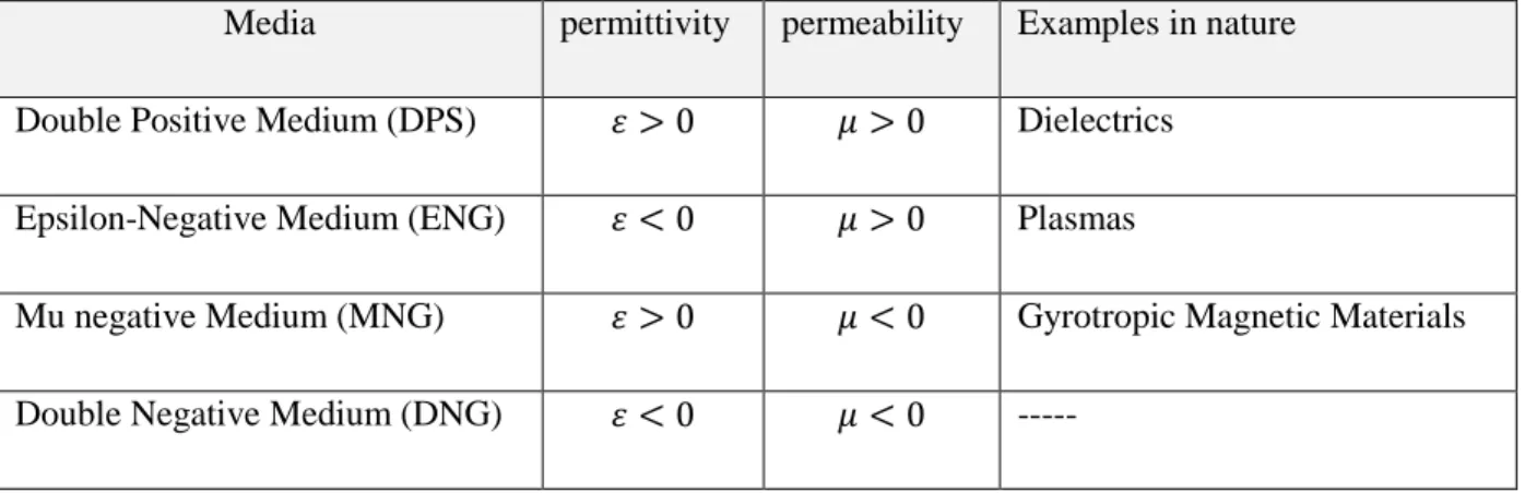
As mentioned in advance, the macroscopic features of the bulk composite, so called “medium,” can be affected by the inclusions which are embedded into it. Relying on a very simple idea meta-materials give the designers and researchers a tremendous amount of degree of freedom for choosing the size and shape of constructions, the properties of the host materials, the composition of the inclusions, the density, arrangement, and alignment of the inclusions above, etc. In the same line of reasoning, they have too many independent parameters to tackle with it. How to assign proper values for all of these parameters brings in many trade-offs regarding efficiency, gain, cost, size, etc., which affect the outcome of the synthesis process extensively. Hence, the optimal choice of these parameters in a great endeavor for both research and industrial institutions. Here is a classification of media based on the pertaining values of permittivity (the ability of a substance to store electrical energy in an electric field) and permeability (a quantity measuring the influence of a substance on the magnetic flux in the region it occupies) provided in [9]. While the magnetic dipoles stem from moments about current loops, they can be described by magnetic charge and
2 | P a g e
current analogs of the electric cases. So materials can be described by their permittivity or permeability considering the scenario and availability of data.
Table 1.1 Material classifications
Media permittivity permeability Examples in nature
Double Positive Medium (DPS) 𝜀 > 0 𝜇 > 0 Dielectrics
Epsilon-Negative Medium (ENG) 𝜀 < 0 𝜇 > 0 Plasmas
Mu negative Medium (MNG) 𝜀 > 0 𝜇 < 0 Gyrotropic Magnetic Materials
Double Negative Medium (DNG) 𝜀 < 0 𝜇 < 0 ---
At certain frequencies, the electric and magnetic fields induced by the inclusions to the host medium can result in negative permittivity and permeability. It is evident that such material does not exist in real nature, but there are certain advantages brought by the discovery of this phenomenon that has made meta-materials very interesting. From a historical point of view, the possibility of a medium having simultaneous negative permittivity and permeability was theoretically back in 1968 [12]. However, authors in [4,5] succeeded in building structures which held simultaneous negative permittivity and permeability or so-called DNGs. In particular, meta-materials enable the flexibility of independently controlling the permittivity and permeability to be almost any arbitrary values. As a result of this phenomenon deep sub-wavelength confinement and focusing of electromagnetic waves in a different spectrum, regimes are easily achievable. In other words, engineers will be able to tune the properties of materials by external stimuli.
1.2 The Scattering Phenomenon
Figure 1.1 represents a normally incident plane wave that scatters from a DNG slab with thickness 𝑑 embedded in a medium. The surrounding area is characterized by {𝜀1; 𝜇1} and {𝜀2; 𝜇2} which illustrate the
3 | P a g e
the incident waveform, the reflection and transmission coefficients of the slab need to be parameterized as per below,
(1)
(2)
where the wavenumber 𝑘𝑖 = 𝜔√𝜇𝑖𝜀𝑖 and wave impedance 𝜂𝑖 = √𝜇𝑖⁄ for 𝑖𝜖{1,2}. In the special case of 𝜀𝑖
matched impedance, where 𝜂1 = 𝜂2, the reflection and transmission coefficients of the slab will be 𝑅 = 0
and 𝑇 = 𝑒−𝑗𝑘2𝑑.
Figure 1.1 The scattering plane wave from a slab with a thickness of d [9].
Knowing that 𝑇 = 𝑒+𝑗|𝑘2|𝑑, the transition of the wave through the slab will lead to adding a positive phase to the phase of the wave. One of the most practical applications of meta-materials is "Phase Compensation" where a matched DNG slab can be utilized to compensate for phase changes induced by passage of a plane wave through a DPS structure. This concept is commonly used in industry. Here is the mathematical representation of Phase Compensation process:
4 | P a g e
To account for a more realistic scenario, oblique incident waves are further discussed. Equations (1) and (2) need to be simply updated by adding transverse impedance and longitudinal wave number components. In the case of an evanescent wave, the transverse wave impedance and the longitudinal component of the wave vector in each medium becomes purely imaginary.
𝜂1𝑡 = 𝑗𝑋1𝑡 (4)
𝜂2𝑡 = 𝑗𝑋
2𝑡 (5)
𝑘1𝑙 = 𝑗𝛼1 (6)
𝑘2𝑙 = 𝑗𝛼2 (7)
Where the superscript 𝑡 in (4) and (5) denotes traverse components, and the superscript 𝑙 in (6) and (7) denotes longitudinal components. To be more specific, an evanescent wave is an oscillating electric and/or magnetic field whose energy is concentrated around the physical location of the source. In other words an evanescent wave does not illustrate the same propagation behaviours as that of an electromagnetic wave. From a mathematical point of view, if a transverse component of the wave vector of the incident wave becomes greater than the wave number of the medium, we end up with an evanescent wave rather than the conventional electromagnetic wave [10,11]. It is worth mentioning that transverse wave impedance in the DPS and DNG media have opposite signs. The full details are explained in [10,11].
By plugging in the additional traverse and longitudinal components into (1) and (2), one would end up with the same results as before for the matched condition; where be 𝑅 = 0 and 𝑇 = 𝑒−𝑗𝑘2𝑙𝑑.
Many phenomena can be justified by this observation. For instance, it is a well-known fact that at the interface between two media tangential components of the electric and magnetic fields should be continuous. This is a corollary of analysis of Maxwell equations. However, if the two media are different types of a DPS and a DNG medium since the permittivity and the permeability of these two media each have opposite signs, the tangential components will be discontinuous at this interface. So the component will be decreasing as it approaches the boundary and it will be increasing on the different medium on the other side of the boundary. In the same line of reasoning, signs can be allocated to 𝛼1 and 𝛼2.
When the evanescent wave reaches the first interface of two media, it is decaying. It trivially follows that 𝛼1< 0 and there will be no refection into the DPS region. However, in order to satisfy the aforementioned
discontinuity condition, the tangential components of the field on DNG domain need to be increasing and 𝛼2> 0. The major advantage of this structure is to compensate for the decay in DPS domain while
5 | P a g e
scenario but different types of waves or media. Engheta in [9] covers a problem in which unlike the previous case, a growing evanescent wave is the study object when an “incident” evanescent wave is approaching a matched semi-infinite PSD-DNG slab. The best approach to solve this problem would be to come up with equations for the reflection and transmission coefficients as per below,
(8)
(9)
In the so-called matched condition, (4) and (5) hold, and 𝑋1𝑡 = −𝑋2𝑡. Hence, 𝑅 = ∞ and 𝑇 = ∞, meaning
that interface resonance at this boundary exists. The Fresnel “reflection” and “transmission” coefficients for an incident evanescent wave hold the same values. In fact, providing a source in front of the interface of semi-infinite matched DNG-DPS domains, a resonant surface wave propagates along the surface, resulting in a field with an infinitely large value.
There exist pervasive analog circuit discussions for the two examples above [10,11]. In fact, the similarity of exciting an L–C circuit at its resonant frequency is discussed in detail. However, they are not brought into this thesis due to lack of space. However, as they move away from the interface, the magnitude of fields decays significantly.
1.2.1 Negative Refraction
By definition, scattering is a physical process where a form of radiation deviates from a straight trajectory due to non-uniformities in the medium that it passes through. Studying the scattering phenomenon when a wave becomes obliquely incident on a DPS–DNG interface “negative refraction” comes up. This phenomenon can be explained in detail by referring to Fig. 1.2 where the electromagnetic boundary conditions need to be maintained.
6 | P a g e
Figure 1.2 The geometry of negative reflection of a wave on a PSD_DNG interface [9]. Using the Snell’s law is a formula used to describe the relationship between the angles of incidence and refraction can be found below:
(10) Since the index of refraction (𝑛 = ∓√𝜇𝜀) of the DNG medium is negative, the refracted angle would be also negative, and consequently it, would be on the same side as that of the incident wave as illustrated in Fig. 1.2.
The wave and Poynting vectors associated with this scenario are given below,
(11)
7 | P a g e
Where the superscripts inc, refl and trans refer to the incident, reflected and transmitted respectively. Due to specific property of DNG media, the Poynting vector and the wave vector will attain different signs and point in different directions which are mathematically represented in (13). In other words, the Poynting will be directed away from the interface.
(13)
1.3 Applications
The research interest in the field of “meta-materials” stems from the fact that the negative refractive index changes the conventional propagation behaviors. For example, Doppler shift is reversed, and Cherenkov radiation is emitted in the opposite direction to the charge’s motion rather than in the forward direction [12]. Here come some of the common applications of meta-materials, however it should be mentioned that their applications are not limited to the following. Sub-wavelength wave guiding, invisible cloaking [13], super lenses [14, 15], imaging and modulation are more technical examples for applications of virtual realized meta-material. For instance, Fig. 1.3 illustrates a three-dimensional (3D) flat lens and its unit cell, with which sub-wavelength resolution imaging can be observed at microwave frequency regime. In recent years, most efforts were focused on the engineering and extension of the functionalities of meta-materials at terahertz [16] and optical [17] frequencies. Details of all of the applications are not brought in here because they are not directly related to the objectives of this thesis.
8 | P a g e
Figure 1.3 A three-dimensional meta-material and a unit cell with a body-centered cubic structure [9].
1.3.1 Phase Compensation with a DNG Medium
One of the main advantages of DNG media is to provide negative refraction and phase compensation is one of the main outcomes about this feature [18]. Let us take the pair of DPS and DNG layers with an index of refraction of 𝑛1 and −𝑛2, and thickness of dDPS and dDNG as depicted in Fig. 1.3. It is assumed that the slabs
are lossless and impedance matched to the surrounding media. What would happen if a monochromic plane wave traverses the concatenation of these slabs configured as? The phase difference that is imposed on the monochromic wave is
𝛥𝛷 = 𝑛1𝑘0𝑑DPS− 𝑛2𝑘0𝑑DNG. (14)
It can be inferred from (14) that the phase difference imposed by the DPS slab can be partially or even totally compensated by the phase difference imposed by the DNG slab. Proper choice of parameters can lead total compensation of the phase, simply by 𝑛1𝑑DPS= 𝑛2𝑑DNG.
At the implementation stage, the size of the composites is usually a great matter of concern that the designers need to tackle with it. However, the previous discussions prove that only the ratio of 𝑑1 and 𝑑2is
important and the size can be engineered based on other limiting parameters of the system, which is quite a big advantage of this technology.
9 | P a g e
Figure 1.4 A pair of DPS and DNG layers sandwiched together.
1.3.2 Meta-materials with Refraction Index of Zero
The application of meta-material is not limited to phase compensation. The ones that hold very low values of permittivity and permeability have fascinating applications as well. They have the potential to exhibit both positive and negative values of the index of refraction near zero and have been experimentally developed in laboratory environments [19-25]. In general, there have been several demonstrations, both theoretically and experimentally, of planar meta-materials that exhibit a zero index of refraction and fall in the intersection of different types of media as illustrated in Fig. 1.4.
In fact, by proper engineering of these zero-index planar materials, it is possible to fabricate high tech resonators, phase shifters, couplers, or similar circuit elements [26]. For instance, by matching the resonances in a series–parallel circuit realization of a DNG, the propagation constant as a function of
10 | P a g e
frequency passes through zero with a non-zero slope in its transition from a DNG domain to a DPS domain in a continuous manner. This operation is specific to a certain frequency of operation and may not illustrate the same results for another frequency [27]. Volumetric materials are another group of meta-materials for which the medium index is approximately zero [28]. These zero-index electromagnetic bandgaps (EBG) are normally excited at a specific frequency which needs to be in the interval of EBG’s passband. To be more specific, when periodic structures interact with electromagnetic waves, characteristics such as frequency stop-bands, pass-bands and band-gaps are introduced. These applications of this observation are seen in filter designs, gratings, frequency selective surfaces (FSS), photonic crystals and band gaps (PBG), etc. They are classified under the broad terminology of “electromagnetic band gaps (EBG)” [29]. One of best outcomes of using this type of material has been for the antenna designers who came up with extremely narrow antenna patterns in [30].
Figure 1.5 The Electrical characteristics for host media with an index of zero (red circle).
Another set of experiments on zero-index meta-materials has been conducted by Ziolkowski at [31], where the propagation and scattering properties of a passive, dispersive meta-material is studied which is matched to free space. The theoretical problems behind this scheme fall into different categories of One-, two-, and
11 | P a g e
three-dimensional problems. Even though there have been extensive contributions to the problems above, only the one- and two-dimensional ones have been validated and confirmed numerically with Finite-Difference Time-Domain (FDTD) simulations. The interesting observation is that the electromagnetic fields in a matched zero-index medium take on a static character in space, but remain dynamic in the time domain. Hence, the underlying physical basis still becomes associated with propagating fields in the local vicinity.
1.4 Meta-materials in Nature
The high loss in the meta-materials at telecommunication and optical frequencies is the main challenge for the engineers in this field. The main sources of loss are the metals, metal alloys or heavily doped semiconductors in those meta-materials. Without controlling or reducing these losses, it is not possible to utilize these unique materials for the state of the art applications. Hence, new materials with relatively low loss are acquired in the industry. The introduction of alternative materials, for example, graphene and transparent conductive oxides (TCOs), can overcome the major bottleneck and shed light on the limitations. Graphene, the two-dimensional atomic crystal, combines its exceptionally high electronic and thermal conductivities, as well as many other Supreme properties, all of which make it highly common for versatile applications. The carrier concentration in TCOs is in the range of 1020~ 1021cm3 , which will convert the
plasma frequency into the near infrared regime for telecom and tactical applications. The outstanding properties of some natural materials, such as graphene and TCOs, have been covered with details in [32-34] with a focus on their tunability feature.
1.4.1 Graphene
Graphene is an allotrope of carbon in the form of a two-dimensional, atomic-scale, honeycomb lattice in which one atom forms each vertex. Due to its outstanding properties, such as mechanical stiffness, strength, elasticity, absorption, very high electrical and thermal conductivity it is given a second name, “Miracle Material.” The combination of impermeability, transparency, and conductivity will make it useful in transparent protective coatings and barrier films, while transparency, elasticity, and conductivity make it applicable in flexible electronics [35]. Based on these super features, Graphene can be a suitable substitution for the material that is used in industry. Not only the features but also easier access to high-quality graphene synthesized by laboratory procedures amend to the continuous growth of its application. Graphene has been proposed as a new platform for plasmon waveguiding at infrared frequencies [36-38] and can be considered as terahertz (THz) meta-material [39]. The earliest update on utilizing Graphene in technology is in manufacturing bendable smartphones as stated by Bloomberg news recently. Graphene synthesis and
12 | P a g e
characterization is a quite complicated task. The implementation methods of Graphene fall into different categories based on their cost, stability, and reliability. Mechanical exfoliation [40], epitaxial growth on metal substrates [41-43], epitaxial growth on silicon carbide [44, 45], and chemical synthesis [46, 47] are the common methods that have been used so far. Fig 1.6 illustrates some of these methods, their cost and the quality of graphene film synthesized by each corresponding method given by [35].
1.4.2 Transparent Conductive Oxides (TCOs)
In essence, TCOs are metal oxides which are widely known because of their specific properties. The main advantage of TCOs is their tunable optical property since a slight change in carrier density in the accumulation layer results in a significant change in the value of dielectric constant if the applied voltage gets properly adjusted. These natural meta-materials are commonly used in manufacturing photovoltaics and flat panel electronic displays. In recent years, TCOs are representative of TCOs in nature [49].
Figure 1.6 Comparison of the methods for Graphene Mass Production.
Introduced as an alternative for plasmonic meta-materials [48]. Indium tin oxide (ITO) and aluminum-doped zinc oxide (AZO) are representative of TCOs in nature [49].
13 | P a g e
1.5 Research Problem and Objectives
Based on the introduction explained in the previous subsections, the main purpose of this thesis is to present two new meta-material unit cells in both microwave and millimeter-wave frequency bands with a controllable refractive index that have the potential to be used in the structure of reconfigurable antennas. The microwave unit-cell will be designed for the frequency of 2.45 GHz, and it will use PIN-diodes to control the refractive index. Additionally, the millimeter-wave unit-cell will be designed for the frequency band of 30 GHz and will use a geometrical approach to control the refractive index. Moreover, as a second objective of the thesis, two paraffin-based dielectric lenses will be fabricated and validated that is necessary for measurement of meta-material unit cells.
DOI : 10.1109/ANTEM.2016.7550155
© 2017 IEEE. Personal use of this material is permitted. Permission from IEEE must be obtained for
all other uses, in any current or future media, including reprinting/republishing this material for
advertising or promotional purposes, creating new collective works, for resale orredistribution to
servers or lists, or reuse of any copyrighted component of this work in other works.
14 | P a g e
C
HAPTERT
WO:
R
ECONFIGURABLEM
ETA-
MATERIALU
NIT-
CELL WITHC
ONTROLLABLER
EFRACTIVEI
NDEX2.1 Introduction
As mentioned in the previous chapter, one of the interesting applications of meta-materials is the beam deflection of planar antennas that provides a very low-profile solution as explained in [53-54]. In this Chapter, a reconfigurable meta-material unit cell with a controllable refractive index is designed for the operating frequency of 2.45 GHz using PIN-diodes. This unit cell has the potential to be incorporated into the substrate of a planar end-fire antenna and provide an effective solution for beam-switching applications.
2.2 Unit-Cell Design
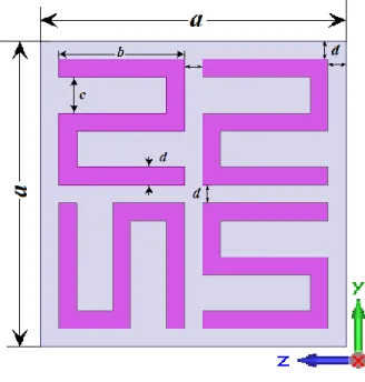
To design a meta-material unit cell with controllable permittivity and permeability, we simply have to pay attention to the position of the cell in the external electric and magnetic field. In fact, a meta-material unit cell should be correctly excited to be able to produce the resonances for producing negative or near zero constitutive parameters. It is important to mention that, in this thesis, the term meta-material is used not only for structures with simultaneously negative permittivity and permeability but also for materials that produce near-zero or very high parameters. Most of the resonant meta-materials use split rings perpendicular to the magnetic field vector and straight lines parallel to the electric field vector. It is evident that a properly excited split-ring plays the role of an inductor (L), while a biased line (parallel to the electric field) behaves as a capacitor (C), and the resonance frequency of such a structure is simply f=1/2π√(LC). To control the behavior of the unit cell, we simply put a loop and also a line in the structure. Therefore, if a PIN diode is embedded in any of these structures, we have the possibility to generate or prevent the resonance by switching the diodes. In the following section, we present a unit cell based on the technique above to provide a controllable response over the frequency range of 1-4 GHz. Figure 2.1 shows a schematic view of our proposed unit-cell. This structure consists of a square-shaped three-turn spiral printed on a Rogers RT/Duroid 5880 with the permittivity of 𝜀𝑟 = 2.2 and the thickness of ℎ = 1.575 mm. Two PIN-diodes are used in the inner and middle rings and a line is printed on the bottom side of the substrate. Spiral resonators are first introduced as meta-material unit cells by Baena et al. in [96-97]. By increasing the number of turns in the spiral unit cell, the overall inductance of the structure and therefore the resonance frequency can be changed. As shown in Fig. 2.1, the number of turns can be controlled by switching the diodes. Here in this thesis for the proof of concept the diodes are replaced by metallic strips and open circuit in the ON and OFF states, respectively. The simulation results are discussed as follows.
15 | P a g e
(a) (b)
Figure 2.1 The Unit-cell geometry. (a) top, (b) bottom.
(Dimensions in millimeters: a=20, b=16, c=12, d=10, e=6, f=1,g=1,h=1)
The unit-cell was simulated in the HFSS software for an incident wave traveling along the Z direction. The electric and magnetic fields of the incident wave are polarized along Y and X directions, respectively. Figure 2.2 shows the complete details of the simulation setup. The same simulation setup has been used in CST Microwave Studio also, to verify HFSS analysis for the unit-cell, and compare the results of the simulated unit cell in both software.
16 | P a g e
Figure 2.2 Simulation Setup (the highlighted walls are set as PEC boundary conditions, and the non-highlighted walls are PMC)
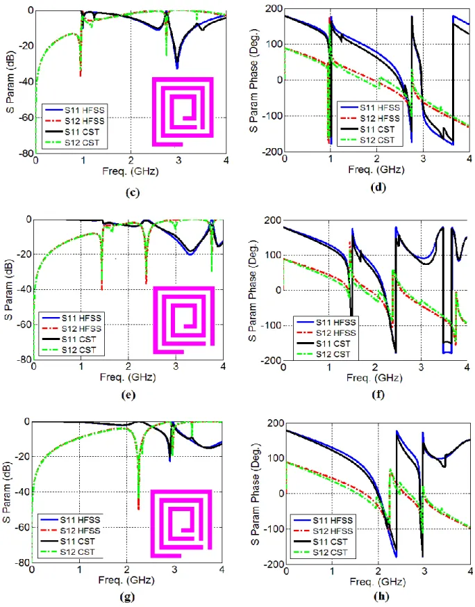
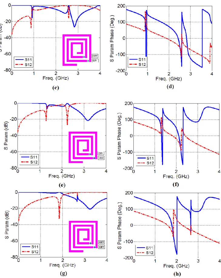
Four different cases are considered regarding the diodes D1 and D2, and all of them were simulated. The simulated S-parameters, resulted from both HFSS and CST are plotted in Figures 2.3 (a)- to (d).
17 | P a g e
Figure 2.3 Simulated S-parameters of the unit-cell when, (a,b) both gaps are closed (c,d) inner gap losed, (e,f) outer gap is closed, and (g,h) both gaps are open.
18 | P a g e
According to Figure 2.3, there is a very good agreement between the results of HFSS and CST. The different configurations of the unit-cell can be discussed as follows. When both of the diodes are ON (Figure 2.3 (a)), the structure has a complete three-turn spiral, and therefore, its inductance is maximum. In this case, because the resonance frequency is inversely related to the product of inductance and capacitance (f=1/(2π√LC)), the frequency of the first resonance in the parameter S12 is the minimum among all the four different configurations. When only one of the diodes is ON, the overall inductance is less than the case above, and therefore the resonance frequency is higher. Finally, when the both of the diodes are OFF the frequency of the first resonance is minimum as shown in Fig. 2.3 (g,h). The simulated S-parameters are used in a well-known algorithm explained in [98] to extract the unit-cell effective refractive index, and the results are plotted in Fig. 2.4. This algorithm is explained in more details in Appendix A.
20 | P a g e
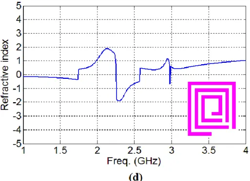
Figure 2.4 Effective refractive index of the unit-cell when(a) both gaps are closed (b) inner gap is closed (c) outer gap is closed (d) both gaps are open.
According to Fig. 2.4, when both of the diodes are ON, the refractive index of the unit-cell is around n=0.5 at 2.45 GHz. This index goes to n=-1 and n=0.6 for Fig. 2.4 (b) and (c), respectively. Finally, when both of the diodes are OFF (Fig. 2.4 (d)), the refractive index at 2.45 GHz shows a value of around n=-1. In other words, the effective refractive index of the unit-cell can be modified by switching the diodes, and a maximum difference of around ∆n=1.5 is achievable at the frequency of 2.45 GHz. This difference can be used for beam-switching applications using reconfigurable meta-materials. This unit-cell will be used for low-profile beam-switching applications.
2.3 Modeling the Diodes
In this section, instead of the ideal scenario for the ON and OFF states of the diodes, a more realistic model is considered, and the effect of this model on the response of the unit-cell is investigated. The PIN-diode that we intend to model is GMP4201 with the lumped element model shown in the figure below.
21 | P a g e
Figure 2.5 Lumped-element model for GMP4201 PIN-diode [54].
The same simulation setup has been used to study the effects of the PIN-diodes, and the results are shown in Figure 2.6 below:
22 | P a g e
Figure 2.6 Simulation results of the diodes using the lumped-element model for the diodes. (a,b) both diodes are ON (c,d) inner diode is ON, (e,f) outer diode is ON, and (g,h) both diodes are OFF.
23 | P a g e
According to the simulation results of Figure 2.6, the diodes result in a downward frequency shift of fewer than 100 MHz in the S-parameters of the unit-cell. This shift can be attributed to the additional capacitance caused by the diodes. It is important to note that other than the frequency shift, the overall behavior of the unit-cell is all configurations remains the same as the ideal scenario.
2.4 Conclusion
In this chapter after introducing reconfigurable meta-materials and discussing different mechanisms that have been designed for implementing them, we introduced a new reconfigurable spiral meta-material unit cell for the frequency range of 1-4 GHz. Two PIN-diodes are used in the structure of the unit-cell and by switching the diodes the refractive index of the unit-cell can be controlled. The results are verified using both HFSS and CST Microwave Studio software. The PIN-diodes are considered first in an ideal scenario and then simulated using a lumped-element model from the datasheet. The results of both scenarios are only different by a frequency shift of fewer than 100 MHz. According to the simulation results, the maximum difference in the refractive index of the different configurations is around ∆n=1.5 at the frequency of 2.45 GHz. The main goal of this framework is to present a feasible solution to implement a simple, low-profile and low-cost agile module with controllable effective constitutive parameters. The possibility of altering the effective refractive index is especially important for us because it can be useful in advanced antenna applications. As already mentioned in this chapter, the resulting agile module has the potential to be used as a detachable part in single element beam-switching antennas that can, in turn, lead to more agile array structures.
DOI : 10.1109/ANTEM.2016.7550179
© 2017 IEEE. Personal use of this material is permitted. Permission from IEEE must be obtained for
all other uses, in any current or future media, including reprinting/republishing this material for
advertising or promotional purposes, creating new collective works, for resale orredistribution to
servers or lists, or reuse of any copyrighted component of this work in other works.
24 | P a g e
C
HAPTERT
HREE:
A
NISOTROPICM
ETA-
MATERIALU
NIT-
CELL FORM
ILLIMETER-W
AVEAPPLICATIONS
(30
GH
Z)
3.1 Introduction
The bandwidth scarcity that is facing wireless carriers has motivated the exploration of the underutilized millimeter wave (mm-wave) frequency spectrum for future telecommunication systems. Coming up with small size devices that operate properly and keep up to daily standards of devices is however quite a big challenge [99]. Despite all the challenges that come up with this transition, there are significant benefits that make it worth a try. The flexible bandwidth rule is one of the main motivations of the industrial branches to move towards this direction [100]. Antenna design has reached to its advanced level after the World War II. However, the designers are still struggling to maintain the same performance levels for mm-wave communication systems using complex methods. The development of the underlying novel components and subsystems necessitates that these components and subsystems be dynamic, reconfigurable and multifunctional. The conventional consumer level world is very familiar with the characteristics of materials and dielectrics, in frequencies like 2.4 GHz and 5.8 GHz. Taking this knowledge as granted, the design and manufacturing of devices for communication systems are esteemed with great expedition. However, in mm-Wave, a tremendous amount of challenge is remaining to understand and characterize the underlying basis of this frequency band. There are new technologies like, electronic band gap (EBG), anisotropic approaches and polarization techniques which are completely opaque and need deep research. One of the recent trends in the modern communication systems is the 5G cellular networks for future mobile phone applications. In fact, there are many speculations regarding all the aspects of this technology from antenna design to the coding systems, and it seems that the frequency range of around 30 GHz is accepted as a feasible band for this technology. One reason for this frequency is that as shown in Figure 3.1, the atmospheric loss at this frequency is low enough to realize the possibility of long range communications.
25 | P a g e
Figure 3.1 Analysis of the atmospheric loss for millimeter wave frequency bands [28].
Therefore, designing an agile antenna system operating over this frequency range can contribute to the design and implementation of future 5G cellular networks. From another point of view, the essential role of meta-materials has been widely covered in the previous sections, though the applications in a combination of high-tech mm-Wave designs have not been covered yet. As emphasized before, meta-material structures have been extensively investigated during the past twenty years, and lots of studies have been done on their properties and applications [4, 101, 102]. Recently meta-material structures have been used for beam-tilting and beam switching applications in microwave and millimeter-wave bands [53, 54]. In all of these cases, the main role of the meta-material medium is to provide a different refractive index than the host medium when interacting with the incident electromagnetic wave. Depending on the application of the antenna, various unit cell structures can be used to provide multi-band, miniaturized or other required features [55, 57]. Using reconfigurable meta-material media [103] is an interesting solution to provide beam-switching for single element antennas. However, reconfigurable unit cells could be lossy and very hard to be implemented at millimeter waves. Another solution that could be potentially useful to solve this problem is to design a medium with two different responses for different propagation directions and then mechanically rotate the structure in the front of the antenna. In this chapter, we present the design and simulation results for an anisotropic unit cell structure that can provide feasible solutions for such applications.
26 | P a g e
3.2 Design and Simulation of the Unit Cells
The key to designing an anisotropic structure is to use a topology which is different if looked at from different directions. Of course, there are various shapes in the nature that might have this property, but not all of them are easy to implement. The S-shaped topology is an easy to fabricate a structure that exhibits the anisotropic property. In this section, we propose the design of an anisotropic meta-material unit cell based on this concept. The schematic view of the proposed unit cell is depicted in Figure 3.2. Four S-shaped conductors with different directions are printed on the top and bottom sides of a Rogers RT/Duroid 5880 substrate with the permittivity of εr=2.2 and the thickness of h=0.508 mm to form this structure.
Figure 3.2 The Unit-cell geometry.
(Dimensions in millimeters: a=2.95, b=1.22, c=0.35, d=0.175)
The overall dimension of the unit cell is 2.95mm, and each S-shaped is around 1.2 mm. This structure operates in two different modes depending on the direction of the incident wave, and each mode provides a different refractive index. The first mode is when the incident wave travels along the Z axis with the electric and magnetic field polarized along the Y and X, respectively. In the second mode, the electromagnetic wave travels along the Y direction, and the electric and magnetic field is polarized along X and Z. Both of these modes are simulated in HFSS, to calculate the S-parameters of the unit cell, using the PEC and PMC boundary conditions along XZ and YZ planes for the first mode, and YZ and XY for the second mode. The complete simulation setup is shown in Figure 3.3 as below:
27 | P a g e
Figure 3.3 The complete simulation setup.
Figure 3.4 plots the HFSS results for the S-parameters of the unit cell in both modes. The simulation frequency range is from 20 GHz to 40 GHz to show the behavior of the structure outside the region of interest (30-35 GHz).
28 | P a g e
(b)
Figure 3.4 Simulated S-parameters for the unit-cell when the wave travels along Z (a) and Y (b). The simulated S-parameters are then used in a well-known algorithm explained in [98] to extract the effective refractive index of the structure in each mode. In this algorithm (which is explained in Appendix A), the S-parameters are used as the reflection and transmission coefficients to compute the effective constitutive parameters. Therefore, studying the S-parameters can give the reader a better insight to verify the behavior of the unit cell. The extracted effective refractive index of the structure is plotted in Figure 3.5 over the frequency range of 30-35 GHz.
29 | P a g e
(a)
(b)
30 | P a g e
According to the results in Figure 3.5, when the electromagnetic wave enters the structure in the Z direction, it sees a near-zero refractive index from 31.5 GHz to 34 GHz while the Refractive index from 30.5 GHz wave arrives from the Y direction, the structure shows an effective refractive index between one and two. As explained in the introduction, this difference can be useful in meta-material-based beam switching techniques. In these applications, an artificial dielectric medium is placed in the front of the antenna to cover only a limited section of the space seen by the antenna radiated wave. This configuration will result in the deflection of antenna beam toward the medium with higher refractive index. The following is a practical scenario about the practical application of our anisotropic meta-material unit cell in beam-switching applications. It is noteworthy of mentioning that in this scenario, the meta-material medium in front of the antenna is independent of the antenna itself and can be considered as a separate beam-tilting unit and therefore it is possible to move or rotate it. Figure 3.6 shows this concept with more details.
Figure 3.6 Separate tilting unit in front of the antenna
As shown in Figure 3.6, the beam tilting unit is composed of two different sections. The factor which is important in beam tilting is ∆n=na-nb. If one of the sections is implemented by the proposed unit cell, we
have the possibility to rotate the structure and obtain two different ∆n, which leads to two different tilt angles or in other words beam switching capability.
31 | P a g e
3.3 Conclusion
In this chapter, the design and simulation of a new meta-material unit cell with the controllable refractive index at 30 GHz are presented. This unit cell has an anisotropic structure that is capable of changing its refractive index when the unit cell is rotated compared to the incident wave. According to the simulation results, this unit-cell can produce a maximum difference of ∆n=2.2 in the refractive index at 32 GHz. Moreover, a qualitatively explained scenario is discussed on the practical use of this unit-cell for beam switching applications.
DOI : 10.23919/EuCAP.2017.7928499
© 2017 IEEE. Personal use of this material is permitted. Permission from IEEE must be
obtained for all other uses, in any current or future media, including reprinting/republishing this
material for advertising or promotional purposes, creating new collective works, for resale
orredistribution to servers or lists, or reuse of any copyrighted component of this work in other
works.
32 | P a g e
C
HAPTERF
OUR:
T
HEF
ABRICATION ANDT
EST OFP
ARAFFIN-
BASEDD
IELECTRICL
ENSES FORM
ETA-
MATERIALM
EASUREMENT4.1 Introduction
Meta-material structures have been extensively investigated during the past twenty years, and lots of studies have been done on their properties and applications [4-121]. Recently meta-material structures have been used for beam-tilting, beam forming and beam switching applications in microwave and millimeter-wave bands as a lens or single media [53, 54]. In all of the previously reported works, the main part of the meta-material medium design is the fabrication and test process to validate the simulation results for the unit-cell. To reach that purpose, the S-parameters resulting from a meta-material cell or medium prototype should be measured. Various methods are used to carry out this type of measurement including the free-space method [114], waveguide method [115] and a series of single-cell methods [116]. Here, we propose a low-cost yet effective method to measure the S-parameters using the free-space method.
In this chapter, the process of fabrication and test of two paraffin-based dielectric lenses that are intended for meta-material measurement is fully described. This analysis is done to certify that the paraffin-based lens can handle high frequencies for meta-material measurement setup, two dielectric lenses are fabricated using a molding process for the frequency range of 10-18 GHz. The fabricated lenses guarantee low cost and ease of implementation compared to the other machining and material methods. Two similar paraffin lenses are used to measure the S-parameters of a conventional SRR meta-material unit cell to verify the proposed lens performance. This experiment confirms a good agreement between simulation and measurement results.
The use of the dielectric lenses as a part of antennas dates back to 1887 when Heinrich Hertz had his first illustration of electromagnetic waves [113]. Just like most of other technologies, it was not until World War II that the research on lens antennas further progressed. Along with all the advantages that this technology brings about, Paraffin lens manufacturing holds a strict guarantee for low-cost implementation. This is one of the main motivations for using Paraffin in this framework.
In the following, the details of the fabrication process are entailed. Next, the measurements and discussion section evaluate the functionality and performance of the fabricated lens.
4.2 Fabrication Process
The material that usually is used to fabricate a dielectric lens is polystyrene microwave plastic or Rexolite [98]. This material has some drawbacks compared to paraffin wax such as high cost of machining process
33 | P a g e
for fabrication, and relatively high density (1.11 g/cm3), which makes the fabricated structure too costly especially for dimensions associated with the C- and S-band applications. In this study, the paraffin wax was used in a molding process as an alternative approach to the lens design and implementation. This material has the permittivity of 2.55, which is very close to Rexolite with better mechanical characteristics to ease the fabrication and shaping, while its density is around 0.88 g/cm3 that makes the structure around 20% lighter compared to plastic-based lenses. To fabricate the lens, we used the molding process, which is proved to be an effective method for the frequency range of 1-4 GHz [120]. The objective of this experience is to determine how much we can increase the frequency range. To make sure that the lens can handle higher frequencies, instead of big reflectors, we used much smaller reflectors with the 12-inch diameter for free space measurement set up that makes the molding process much more accurate. The reflectors are parabolic reflector bought from EdmondOptics company, and they provide a double convex profile for the lens. Moreover, we can control that the surface of the lens is smooth enough, which is necessary for high-frequency applications. The other precaution that we did is to buy all the needed wax at once; this makes sure that the whole amount of wax has the same characteristics. In the previous experiment because of the high volume of the wax, it was impossible to buy all of it at once, and therefore the resulting structure had several layers. Figures 4.1 - 4.3 show the process of molding as well as the lenses at their final stage.
34 | P a g e
Figure 4.2 The fabricated lenses.
Figure 4.3 Close view of the fabricated lens.
4.3 Measurement and Discussion
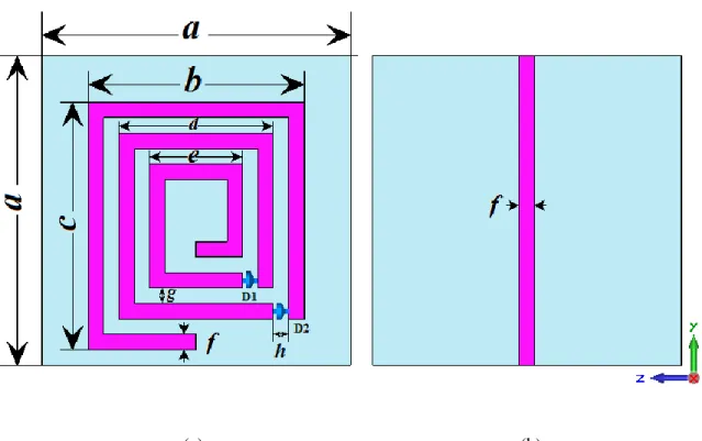
In this experiment, we measured the S-parameters of three conventional SRR (Split-Ring Resonator) and line combinations with different dimensions for three frequency bands. These bands are 1-4 GHz, 5-13 GHz, and 10-18 GHz that we name them "low-frequency," "middle-frequency" and "high-frequency"
35 | P a g e
respectively. As shown in Figure 4.4, the unit cells are printed on top and bottom of a Rogers 5880 substrate with the thickness of 1.575 mm (for the low-frequency unit cell) and 0.508mm (for middle and high-frequency ranges).
Figure 4.4 Split-Ring Resonator Unit-cell
(a) Schematic view, (b) Low-frequency unit-cell, (c) middle-frequency unit-cell, (d) High-frequency unit-cell
The dimensions of the SRR unit cell for each frequency are listed in Table 4.1, and a photograph of the test setup can be found in Figure 4.5.
Table 4.1 The geometrical parameters of the SRR unit cell layout. Parameter (mm) Low-Frequency Middle-Frequency High-Frequency
a 18 4.5 3
b 15 3.75 2.5
d 1.5 0.375 0.3
g 1.6 0.4 0.3
36 | P a g e
Figure 4.5 Test setup located in INRS-EMT.
To perform the measurement process, first, the low-frequency unit cells in the range of 1-4 GHz were tested to verify the overall performance of the setup. Then we expanded the range up to 12.5 GHz, and finally, we conducted the measurements up to 18 GHz, which is the utmost limit of the horn antenna. The results are illustrated in Figures 4.6 – 4.11.
37 | P a g e
(a)
(b)
38 | P a g e
(a)
(b)
39 | P a g e
(a)
(b)
40 | P a g e
(a)
(b)
41 | P a g e
(a)
42 | P a g e
(a)
(b)
43 | P a g e
As plotted in Figures 4.6 – 4.11, in the low- and middle-frequency bands there is a very good correlation between the simulation and measurement. However, when we go to the high-frequency band, the difference between measurement and simulation becomes more significant. Nevertheless, we can infer from the results that the lens structure works very well up to 12 GHz and then from 12 GHz to 15 GHz the results are acceptable, but for anything higher than that, the results are not good enough. As a reason for this difference, we can point to large dimensions of the horn which causes the spill-over problem and also the inherent loss of the paraffin material at higher frequencies for this application. Nevertheless, we enhanced the upper-frequency limit of our previous work from 4 GHz to 15 GHz, and it seems that it is the final limit for this type of measurement. If we wanted to go higher than this limit, the cost of the project would be too high to justify this method.
It is important to mention that the phase of the S-parameters are as important as the magnitude and it is necessary to measure them too because, in the extraction algorithm, we need the S-parameter as a complete complex number to be able to calculate the effective constitutive parameters. That is why we included the measurement results for the phase to show that our lens structure is capable of producing accurate results in terms of phase. Of course, there is a calibration procedure that we have followed in all of the measurements, and it is explained in Appendix B in more details.
4.4 Conclusion
We fabricated two paraffin-based lenses for meta-material measurement. Compared to the previous set of lenses made in the group (in the range of 1-4 GHz), we used smaller structures, and the fabrication process was done much more accurately, and the results are acceptable up to 15 GHz. However, when we go higher than that (up to 18 GHz which is the horn upper-frequency limit), the measurement results show a significant difference compared to the simulations. As some of the reasons for this difference, we can point to large dimensions of the horn which causes the spill-over problem and also the inherent loss of the paraffin material used for this application. Nevertheless, we enhanced the previous design from 4 GHz to 15 GHz, and it seems that it is the limit and if we wanted to go higher the cost of the project would be too high.
44 | P a g e
C
HAPTERF
IVE:
C
ONCLUSION ANDF
UTUREW
ORK5.1 Introduction
In this Chapter, a brief summary of the three research topics conducted in the context of this thesis is presented. Also, the links between these concepts are explained in more details. Moreover, the future direction of this research is discussed.
5.2 Antenna Applications
As already mentioned in the previous chapters, the main subject of this thesis is the design and simulation of innovative meta-material unit cells. Of course, because this research is done in the framework of a master degree in telecommunications, it is necessary to define some practical applications for the aforementioned unit-cells. On the other hand, in recent years, extensive research has been conducted at INRS-EMT on the topic of meta-material-inspired reconfigurable antennas. Therefore, it has been decided that I somehow show that my new meta-material unit cells can serve this purpose. However, from the beginning, we had decided that the design and implementation of a reconfigurable antenna are well beyond the scope of this master thesis and only some qualitatively explained scenarios suffice to show the whole purpose of my meta-material unit cells. That is why a PIN-diode-based reconfigurable meta-material unit cell along with another anisotropic unit-cell are presented in this thesis. Moreover, the idea of how an anisotropic structure can be helpful in beam switching applications is one of my contributions that is explained at the end of Chapter 3.
5.3 Meta-material Structures in the Millimeter-wave band
Today, it is widely accepted that the millimeter-wave frequency band is the future of modern communication systems. There are lots of areas that millimeter waves can be helpful, ranging from indoor Gbps wireless LANs to future 5G cellular networks and deep-space communications. Therefore, it has been decided that a part of this research should be focused on the millimeter waves and to investigate how practical it is to use meta-material unit cells in this frequency band. However, using reconfigurable elements such as PIN-diodes in millimeter-waves is very expensive and challenging. For this reason, I have presented
45 | P a g e
the idea of an anisotropic meta-material unit cell at 30 GHz. If you mechanically rotate this structure, it can produce a different refractive index in each position.
In other words, having two different refractive indexes is the main goal of our design what we need to perform the beam switching, and both of the presented unit cells are capable of providing this feature, one of them by switching the PIN-diodes and the other one by mechanically rotating.
5.4 Dielectric Lenses for Meta-material Measurement at Millimeter Waves
The final topic of this research is fabrication and validation of two paraffin-based dielectric lenses that are necessary for meta-material measurements. A low-frequency version of these lenses has already been implemented by a former Ph.D. student of INRS-EMT [35]. However, his structure was only capable of providing reliable results up to 4 GHz. On the other hand, one of my research topics in this thesis was to work in the millimeter-wave frequency band. So it was necessary to implement a dielectric lens to enhance the limit of 4 GHz. For this reason, two paraffin-based lenses were fabricated. It is clear that for validating these lenses, a well-known structure had to be used because the simulation results of the unit-cell have to be used for validation and we should be familiar with those results. For this purpose, a simple SRR (Split-Ring Resonator) unit-cell is fabricated in three different sizes, and all of them are tested using the lens. According to my results, the fabricated dielectric lenses are capable of providing reliable results up to 15 GHz. In other words, I have improved the frequency limit from 4 to 15 GHz.
5.5 Future works
Based on the research conducted in this thesis, I propose three main future directions. The first one is working on new reconfiguration techniques that are capable of being implemented at millimeter waves such as MEMS. Another interesting direction is the combination of the anisotropic geometrical technique with reconfigurable elements that can be helpful in adding more agility to the unit-cell structure. Finally, the scenario of mechanically rotating the meta-material section in front of the antenna has a great potential to be used with innovative antennas in both microwaves and millimeter-wave frequency bands.
46 | P a g e
5.6 Conclusion
This thesis presents two new meta-material unit cells that are both capable of providing a controllable refractive index which is necessary for the beam switching technique that is developed in our groups by former students in the recent years. One unit-cell is designed in the frequency range of 1-4 GHz and utilizes PIN-diodes to control the refractive index. This unit-cell is capable of providing a difference of ∆n=1.5 in the refractive index at 2.45 GHz. The other unit-cell is designed at 30 GHz and has an anisotropic behavior which results in the capability of controlling refractive index by rotation. According to our simulation results, this unit-cell can produce a difference of ∆n=2.2 at 32 GHz. Moreover, a possible scenario about how this unit-cell can be useful in beam switching is qualitatively explained. Finally, as a marginal product of my research, two dielectric lenses for meta-material measurements are fabricated and experimentally verified. These lenses are far better than the previous lenses developed in our group and increase the frequency limit from 4 to 15 GHz.
![Figure 1.2 The geometry of negative reflection of a wave on a PSD_DNG interface [9].](https://thumb-eu.123doks.com/thumbv2/123doknet/5006174.124931/16.918.175.744.141.429/figure-geometry-negative-reflection-wave-psd-dng-interface.webp)
![Figure 1.3 A three-dimensional meta-material and a unit cell with a body-centered cubic structure [9]](https://thumb-eu.123doks.com/thumbv2/123doknet/5006174.124931/18.918.154.781.119.449/figure-dimensional-meta-material-unit-centered-cubic-structure.webp)
![Figure 3.1 Analysis of the atmospheric loss for millimeter wave frequency bands [28].](https://thumb-eu.123doks.com/thumbv2/123doknet/5006174.124931/37.918.189.668.130.507/figure-analysis-atmospheric-loss-millimeter-wave-frequency-bands.webp)