Structural analyses by advanced X-ray scattering on GaP layers epitaxially grown on silicon for integrated photonic applications
Texte intégral
Figure


Documents relatifs
In order to investigate the refractive index as a function of the light sources used for the photolithography and the impact of the photo-initiator, we have used the M-line
Further analysis including the correction for absorption, air scattering, fluorescent radiation, multiple scattering and Compton scattering has been made with respect the the
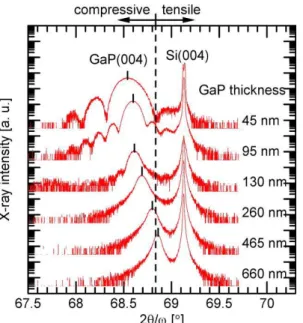
The refinement of the structure must be done by including reconstruction/relaxation in the underlying Si-substrate, but the main features contained in the x-ray
In particular the intensity of the gap state emission relative to the main band is unchanged a s time (and contamination) proceeds. Comparing the intensity from
dination. The Bhatia-Thornton partial structure factors are then deduced. From the partial radial distribution functions the partial coordination numbers are calculated
In this case, the pseudo-solid, coexisting with a low-density phase, can be strongly compressed; the molecules lay certainly flat on the graphite at first and
The first observations of smectic layering free surface in liquid crystals in the nematic phase [6-8] involved only one layer spacing and in comparison to figure 3 only
Sketch of the Si and GaN reciprocal lattice in the plane of diffraction (hkl notation is also used for the hexagonal GaN lattice). The reflections used for the de- termination of
