HAL Id: pastel-00000621
https://pastel.archives-ouvertes.fr/pastel-00000621
Submitted on 16 Apr 2004
HAL is a multi-disciplinary open access archive for the deposit and dissemination of sci-entific research documents, whether they are pub-lished or not. The documents may come from teaching and research institutions in France or abroad, or from public or private research centers.
L’archive ouverte pluridisciplinaire HAL, est destinée au dépôt et à la diffusion de documents scientifiques de niveau recherche, publiés ou non, émanant des établissements d’enseignement et de recherche français ou étrangers, des laboratoires publics ou privés.
d’Arséniure de Gallium par sondage électro-optique
utilisant un faisceau laser continu
Stefan Lauffenburger
To cite this version:
Stefan Lauffenburger. Caractérisation des circuits intégrés micro-onde à base d’Arséniure de Gallium par sondage électro-optique utilisant un faisceau laser continu. domain_other. Télécom ParisTech, 2003. English. �pastel-00000621�
présentée pour obtenir le grade de docteur de l’École Nationale
Su-périeure des Télécommunications
Spécialité: Électronique et Communications
Stefan Lauffenburger
Caractérisation des circuits intégrés micro-onde à base d’Arséniure
de Gallium par sondage électro-optique utilisant un faisceau laser
continu
( Characterization of microwave Gallium Arsenide integrated circuits with
electro-optic probing using a continuous laser beam )
Soutenu le 21 Février 2003 devant le jury composé de
Georges Alquié
Président
Lionel Duvillaret
Rapporteurs
Smaïl Tedjini
Georg Guekos
Examinateur
Didier Erasme
Directeurs de thèse
Cassius Longinus, Greek rhetorician and philosopher.
Remerciements
Je tiens à exprimer en quelques mots ma reconnaissance aux personnes qui m’ont aidé avec leurs soutiens scientifiques, techniques et moraux. Sans eux, cette thèse n’aurait jamais vu le jour. J’adresse tout d’abord mes remerciements à Georges Alquié (Professeur à l’Université Pierre &
Marie Curie) pour avoir présidé le jury. Toute ma gratitude va aux rapporteurs Lionel Duvillaret
(Maître de Conférence à l’Université de Haute Savoie) et Smaïl Tedjini (Professeur à l’École
Supé-rieure d’Ingénieurs en Systèmes Industriels Avancés Rhône-Alpes) pour avoir relu attentivement le
rapport et pour leurs remarques constructives. Je tiens également à exprimer ma profonde gratitude envers Georg Guekos (Professeur à l’École Polytechnique Fédérale de Zurich) pour m’avoir donné l’opportunité de faire une thèse à Paris, pour ses commentaires enrichissants et pour avoir accepté d’être examinateur dans le jury.
Je veux aussi remercier les responsables de l’ENST pour m’avoir donné la possibilité de réaliser ce travail. En particulier, il y a Didier Erasme et Bernard Huyart qui ont surveillé mes activités, Guy Debarge qui m’a aidé avec les calculs mathématiques, Claude Chabran, Renaut Gabet, et Yves Jaouën qui m’ont soutenu pendant la réalisation de l’expérience , Xavier Begaud qui a mis à dispo-sition des logiciels de simulations micro-onde et Alain Croullebois qui a fabriqué les montages mé-caniques.
J’aimerais aussi exprimer ma reconnaissance pour l’aide financière du Conseil de bourse de ABB et de la Conférence des Recteurs des Universités Suisses.
Je ne peux pas m’abstenir de mentionner les aides précieux des “supports techniques” de "National Instruments", "Agilent" et "Keithley" qui ont répondu à beaucoup de questions très particulières. J’aimerais aussi salué tous les autres thésards et stagiaires qui étaient à l’origines de la bonne am-biance indispensable à la réalisation d’un travail scientifique. Je commence par ordre chronologique: Amal pour m’avoir initié aux problèmes d’une “thésarde abandonnée”, Olivier pour avoir éclairé avec ses “halos” notre bureau sombre, Céline et Sandrine pour leurs gâteaux, Catherine et François-Xavier pour leur introduction à “l’art de vivre” à la française, Christophe Brutel pour ses renseigne-ments informatiques et Loïc pour sa bonne humeur. Je suis reconnaissant pour le soutien informati-que et moral de Cédric accompagné de sa cannette “Coca Light” posant des informati-questions métaphysiques. Le calme de nos deux mexicains (Carlos et Gabriel) m’a beaucoup inspiré dans les situations difficiles. La réalisation de la manipe était facilitée par le fait que Helena, Lydia & Virgi-nie ne m’ont que rarement enlevé de l’équipement mais m’ont rendu d’autres services. Il m’a été d’une grande aide de toujours pouvoir récupérer mes affaires à proximité des trous noirs du labo gé-rés par Christophe Gosset en colaboration avec Joseph Désiré. La rédaction du rapport était devenue seulement supportable par mes deux superbes collègues de bureau (Sabine et Ghaya) qui m’ont ren-du beaucoup de services. J’aurais presque oublié “l’inoubliable” stagiaire allemande (Petra) qui m’a donné beaucoup de confiance. Je devrais ajouter encore beaucoup de lignes pour d’autres personnes (Ali Reza, Anne-Claire, Béatrice, Bruno, David, Fabien, Hedi, Ines, Jérémie, Georgia alias Yolada, Laurent, Mariam, Mohamad, Sébastien, Souheil et al.), mais j’ai bien peur qu’il ne manque encore une fois du papier dans l’imprimante....
Abstracts
Abstract
The number of microwave inte-grated circuits (IC) has increased in recent years following the trend towards higher carrier frequen-cies. This kind of IC is commonly
used in telecommunications
where they can be found in cellu-lar phone equipment or in devices for satellite communications. The possession of simulation software and probing tools is vital for fur-ther development of such ICs. These tools can localize the criti-cal points in the IC and so the
de-sign can be improved.
Considering that an IC has a limit-ed number of input and output ports, it is rather difficult to char-acterize the electrical signal inside an IC. Several different probing techniques based on different ap-proaches were proposed and de-veloped recently.
In this thesis we focus on the prob-ing of Microwave Monolithic In-tegrated Circuits (MMIC) made of Gallium Arsenide (GaAs). The basic idea is to exploit the electro-optic properties of the semicon-ductor. We focus a laser beam onto the Device Under Test (DUT). Considering that GaAs is
“transparent” for the chosen
wavelength, a part of the laser beam will enter the substrate and will be reflected from the back face of the device. The reflected laser beam will be modulated in
Résumé
Pendant les dernières années le nombre de Circuits Intégrés (CIs) micro-ondes a fortement aug-menté suite à l’utilisation de fré-quences porteuses de plus en plus élevées. Ces types de CI sont très fréquemment utilisés dans les télécommunications, dans l’équi-pement pour des téléphones porta-bles ou pour la communication satellite. Pour le développement et l’amélioration des CIs, il est important d’avoir à disposition des outils de mesure et de simula-tion. Avec ces outils, on peut loca-liser les points critiques et la
con-ception peut être améliorée.
Considérant que le nombre
d’entrées et de sorties d’un CI est limité, la mesure des signaux élec-triques dans un CI est une tâche délicate. Plusieurs techniques de mesure ont donc été proposées ces derniers temps ou sont en cours de développement.
Cette thèse est centrée sur le
son-dage des circuits Microwave
Monolithic Integrated Circuits
(MMIC) à base d’Arséniure de Gallium (AsGa). L’idée princi-pale est d’exploiter les propriétés électro-optiques du semiconduc-teur. Un faisceau laser est focalisé sur le circuit testé. Considérant que le AsGa est “transparent” pour la longueur d’onde choisie, le faisceau entre dans le compo-sant et il se réfléchit sur la face arrière. Le faisceau réfléchi est modulé en fonction du signal micro-onde recherché car les
pro-Zusammenfassung
Als Folge der immer höheren Trä-gerfrequenzen hat die Anzahl von Integrierten Schaltungen (IS) bei Mikrowellenanwendungen in letz-ter Zeit stark zugenommen. Häufig werden solche IS in der Telekom-munikation eingesetzt, zum Bei-spiel in Mobilfunktelefone oder für Satellitenkommunikation. Für die Weiterentwicklung solcher Schalt-kreise ist es wichtig über geeignete Simulations- und Meßinstrumente z u v e r f ü g e n . S o k ö n n e n d i e Schwachstellen der Schaltungen lo-kalisiert und behoben werden. Da IS nur über eine beschränkte An-zahl von Ein- und Ausgänge verfü-gen, ist es eine schwierige Aufgabe, die elektrischen Signale in den IS zu messen. Mehrere verschieden Meßmethoden für das charaktersie-ren von IS basiecharaktersie-rend auf unter-schiedlichen Ansätzen existieren oder sind in Entwicklung.
In dieser Doktorarbeit konzentrie-ren wir uns auf das Ausmessen von “Microwave Monolithic Integrated Circuits” (MMIC) auf der Basis von Galliumarsenid (GaAs). Die Grundidee ist, die elektro-optische Eigenschaft des Halbleitermaterials GaAs auszunutzen. Dazu wird ein Laserstrahl auf die auszumessende Schaltung fokussiert. Da GaAs für diese Wellenlänge “durchsichtig” ist, wird ein Teil des Laserstrahls erst an der Rückseite des Halblei-ters reflektiert. Der reflektierte La-serstrahl wird in Funktion des gesuchten Mikrowellensignals mo-duliert, da die optischen
Eigen-function of the microwave signal sought after as the optical proper-ties of the GaAs substrate depend on this parameter. We can measure this modulation and hence we can determine the microwave electric field inside the device.
The goal of this thesis is the con-struction of a prototype of a probing tool based on previous work in our laboratory. The aim is a simple set-up with low material costs. As a consequence we use only standard equipment. The essential improve-ment of the presented work is the use of new and more powerful equipment. Explicitly we use polar-ization maintaining fibers, we avoid all free space setups and we review the acquisition software. Further-more we have a look at some theo-retical problems neglected in the previous thesis e.g. we calculate the influence of the electric field direc-tion on the probing results.
In this thesis, we describe the devel-opment of the probing tool as well as the obtained results. We demon-strate the agreement between the experimental measurements and the theoretical description. We show that we can probe the microwave signal with a sensitivity of about and that the opera-tional frequency of the probing tool is only limited by the characteristics of the photodiode and the corre-sponding amplifier. On the other hand, we analyze the major techni-cal problems. Therefore we men-tion the variamen-tion in power and polarization of the laser source used for probing and we analyze the problems of adequately focusing the laser beam onto the IC.
2 mV[ ⁄ Hz]
priétés optiques de l’AsGa dépen-dent de ce paramètre. Nous pou-vons mesurer cette modulation et nous pouvons en déduire le champ électrique dans le CI.
L’objectif de cette thèse est la cons-truction d’un prototype basé sur des travaux précédents réalisés dans notre laboratoire. Le but principal est une conception simple avec des coûts de matériel faibles. Par consé-quent on n’utilise que des compo-sants standards. Le progrès de la thèse présentée est l’utilisation d’équipements nouveaux nettement plus performants. En particulier on utilise des fibres à maintien de pola-risation, on évite toutes les manipu-lations du faisceau laser en espace libre et on renouvelle les logiciels d’acquisition. De plus on traite
quelques problèmes théoriques
négligés dans les travaux précé-dents: par exemple, on vérifie la validité de nos résultats de sondage si la direction du champ électrique n’est pas connue exactement. Dans cette thèse nous décrivons le développement de l’outil et les
résultats correspondants. Nous
démontrons que les résultats mesu-rés correspondent avec la descrip-tion théorique. Nous illustrons que nous pouvons mesurer un signal micro-onde avec une sensibilité
d’environ et que la
fréquence opérationnelle de l’outil de sondage est seulement limitée par les caractéristiques de la photo-diode. Un autre objectif de ce tra-vail fut de trouver les limites tech-niques et leurs origines. Dans ce contexte nous avons dû constater la dépendance de la polarisation et de la puissance de la source laser en fonction de la longueur d’onde. Nous analysons le problème de la focalisation adéquate du faisceau laser sur le CI.
2 mV[ ⁄ Hz]
schaften von GaAs von diesem Parameter abhängen. Diese Modu-lation kann ausgemessen werden und so kann das elektrische Signal bestimmt werden.
Das Ziel dieser Doktorarbeit ist die Realisierung eines Prototypen eines Meßgeräte basierend auf vorherge-henden Arbeiten. Da das Meßgerät möglichst einfacher sein soll, und die Materialkosten niedrig gehalten werden müssen, werden nur Stan-dardkomponenten eingesetzt. Die Neuerungen bei dieser Arbeit sind der Einsatz von aktueller, leistungs-fähigerer Ausrüstung: Es werden polarisationserhaltende Glasfasern eingesetzt, die Laserstrahlmanipu-lationen im freien Raum werden vermieden und die Computerpro-grammierung der Instrumente wird verbessert. Zusätzlich schließen wir noch einige Lücken in der Theorie: Wir berechnen den Einfluß auf die Meßresultate, wenn die Richtung des zu messenden elektrischen Fel-des nicht genau bekannt ist. In der vorliegenden Arbeit be-schreiben wir die Entwicklung des Meßgerätes und die erzielten Er-gebnisse. Wir zeigen, daß die expe-rimentellen Resultate weitgehend mit der theoretischen Beschreibung übereinstimmen. Wir demonstrie-ren, daß wir ein Signal mit einer
Sensitivität von
aus-messen können und daß die maxi-male Arbeitsfrequenz nur durch die Eigenschaften der Photodiode und dem dazugehörigen Verstärker be-grenzt werden. Wir erörtern die we-sentlichen technischen Probleme und ihr Ursprünge: Dazu zählen die Charakteristik der Laser-Quelle (Variation der Leistung als auch der Polarisation). Eine weitere Schwie-rigkeit war das adäquate Fokussie-r e n d e s L a s e Fokussie-r s t Fokussie-r a h l s a u f d i e Schaltung.
Contents
Remerciements ... v
Abstracts ... vii
Contents ... ix
Introduction ... 1
1.
Requirements for Probing
1
1.1. Requested Information 1 1.2. General qualities for probing 22.
Several methods for chip characterizations
4
2.1. Probing with a mechanical tip 4 2.2. Probing with an antenna 5 2.3. Optical probing of Silicon CMOS integrated circuits 5 2.3.1. Hot luminescence technique 5 2.3.2. Laser Voltage Probing 7 2.4. Electron Beam Probing 8 2.5. Sampling Force Probing 9 2.6. External Electro-Optic sampling 10 2.7. Internal Electro-Optic Sampling 12 2.7.1. GaAs based devices and MMIC (Microwave Monolithic Integrated Circuits) 12 2.7.2. Internal probing 13 2.8. Project for the thesis 14Theory ... 15
3.
Electro-Optic Effect
15
3.1. General description of the problem 15
3.1.1. Isotropic and Anisotropic Material 15
3.1.2. Electro-Optic properties of Materials 16
3.1.3. Principle of the Ellipsoid 18
3.1.4. Representation as an ellipsoid 20
3.1.5. Classification of different Anisotropic Materials 21
3.2. Refractive index for different direction of the electric field in GaAs 22
3.2.1. Ex 22
3.2.2. Ey 23
3.2.3. Ez 24
3.2.4. Ex + Ez 25
3.3. Comment 26
4.1. Response of a Fabry Perot Cavity 27
4.2. Minima and Maxima of the Cavity Response 29
4.3. Comment 30
5.
Amplitude Modulation
31
5.1. Modulation caused by the electro-optic crystal 31
5.2. Modulation for a laser polarization not parallel to optical axis 33
5.3. Modulation for an electric field Ex+Ez 34
5.4. Comment 36
6.
Polarization modulation
37
6.1. Setup 37
6.2. Modulation 37
6.2.1. Polarization modulation with a wave plate 39
6.3. Comment 40
7.
Phase modulation
41
7.1. Setup 41
7.2. Comment 42
8.
Other considerations & Problems
43
8.1. Gaussian beam 43
8.2. Spot Size and spatial resolution 46
8.2.1. Spot size without cavity 47
8.2.2. Spot Size on the device 48
8.2.3. Modified Calculation for the Fabry Perot Cavity 50
8.3. Magnitude of the electric fields 52
8.4. Choice of the wavelength of the laser beam 53
8.5. Comment 54
9.
Conclusion of the Theory
55
Measurements ...57
10.
Characterization of the Components
57
10.1. Characteristics of the laser 58
10.1.1. Measurement setup 58
10.1.2. Results 59
10.2. Characteristics of the circulator 60
10.2.1. Measurement setup 60
10.2.2. Results 61
10.3. Characteristics of the focuser 62
10.3.1. Measurement setup 62
10.3.2. Results 62
10.4. Comment 63
11.
Measurement of the Fabry Perot Cavity Response
64
11.1. Measurement for different magnification factors 64
11.1.1. Measurement setup 64
11.1.2. Results 64
11.2. Measurement of the different reflections with a optical reflecto-meter 66
11.2.1. Measurement Setup 66
11.2.2. Results 66
11.3. Comment 68
12.
The electro-optic signal
69
12.1.1. Measurement Setup 69
12.1.2. Results 69
12.2. The electro-optic signal for different directions of the polarization 71
12.2.1. Measurement Setup 71
12.2.2. Results 72
12.3. Linearity and the Signal to Noise Ratio 73
12.3.1. Measurement Setup 73
12.3.2. Results 74
12.4. Comment 77
13.
Mapping of the electric field in a MMIC
78
13.1. Measurement of the electric field beside a microwave guide 78
13.1.1. Measurement Setup 78
13.1.2. Results 78
13.1.3. Simulation 79
13.2. Mapping of the electric field on a chip 80
13.2.1. Measurement Setup 80
13.2.2. Results 80
13.3. Comment 81
14.
Measurement of the S-parameters
82
14.1. Measurement Setup 82
14.2. Results 83
14.3. Comment 84
15.
Signal processing with Stimulated Brillouin Scattering
85
15.1. Principles of Stimulated Brillouin Scattering 86
15.1.1. Spontaneous Brillouin Scattering 86
15.1.2. Stimulated Brillouin Scattering 86
15.2. Verification of the threshold and spectrum of the lightwave 88
15.2.1. Measurement Setup 88
15.2.2. Results 90
15.3. Modulation depth enhancement and the Signal to Noise Ratio 91
15.3.1. Measurement Setup 91
15.3.2. Results 92
15.4. Application of the Brillouin scattering in the probing setup 94
15.4.1. Measurement Setup 94
15.4.2. Results 94
15.5. Comments 96
16.
Conclusions of the Measurements
97
Conclusion ... 99
References ... 101
17.
Books and Thesis
101
18.
Publications, Journals and Proceedings
101
18.1. Optical probing of Silicon CMOS chips 101
18.2. Electron Beam Probing 102
18.3. Scanning Force Probing 102
18.4. Electro-Optic Probing 102
18.5. External Electro-Optic Probing 103
18.6. Internal Electro-Optic Probing 103
18.8. Other References 104
19.
Internet/Electronic Data
104
Appendix ...105
A.
Constants
105
A.1. General Constants in Vacuum 105
A.2. Material Constants 105
B.
Acronyms
109
C.
Symbols
110
D.
Units
111
D.1. Optical Units 111
D.2. Electrical Units 111
D.3. Relation of Electrical and Optical Units 113
E.
Calculations
115
E.1. Calculation of the eigenvalues 115
E.2. Calculation of the eigenvectors 116
E.3. Calculation of reflection and transmission coefficients 119
E.4. Calculation of the Cavity response 121
E.5. Calculation of the partial derivative 122
E.6. Calculation of the Minimum and Maximum of the Fabry-Perot Cavity response
123
E.7. Calculation of the relation between the reflection and R and r 124
E.8. Calculation of the modulation for a polarization between the optical axis 126
E.9. Calculation of the modulation for E=Ex+Ez 127
E.10. Calculation of the Polarization Modulation 130
E.11. Calculation of the Polarization Modulation with two l/8 wave plate 132
E.12. Calculation of the phase shift modulation 134
E.13. Calculation of the Gaussian beam in free space 135
E.14. Spot Size of our probing device 138
Introduction
In the last few years, the use of electronic equipment increased constantly following the rapid de-velopment of computer technology, mobile phones and satellite communication. The steady trend towards faster and more powerful equipment as well as the limitation of frequency forced a devel-opment toward higher and higher frequencies. Hence numerous new electronic applications ap-peared and the part of microwave devices grew quickly.
For the development, design and production of new integrated electronic devices, it is important to have powerful design and probing tools to characterize your new device. There are several possibil-ities to determine the characteristics of an Integrated Circuit (IC). First you can connect your Device Under Test (DUT) to electronic measurement equipment like a network analyzer or similar. Unfor-tunately modern integrated devices consist of a large number of integrated elements and provide a rather small number of output and input pins for external connections. So there are a lot of functions you cannot verify this way. Another method to analyze the characteristics of a DUT is to use a com-puter to simulate the operation of the device. Apart the fact that your device might be too compli-cated or not suitable for a simulation, you have to consider that the software will fail to find a problem if the simulator does not take into account the corresponding (known or unknown) physical effect. The third approach of characterizing an ICis to measure the electric signal inside the semi-conductor. This sounds simpler than it is in reality because integrated devices are so complex that you have to have sophisticated probing techniques to find and acquire your signal.
Parallel with the development of new semiconductors devices, new probing techniques appeared. These new techniques can probe the electric signal inside the IC. Hence they allow improving the actual design. They can also provide the data to improve the electrical models of the simulation soft-ware.
By probing a semiconductor device, you are looking for some specific information or signal data. In this chapter we will first have a look at the different kind of information, you can acquire by prob-ing. We will indicate the general condition for the data acquisition. Afterwards we will investigate several “state of the art” probing techniques.
1 Requirements for Probing
1.1 Requested Information
Before we discuss the different measurement techniques, we should think what kind of information we want to acquire with our measurements. Depending on our goal we might have different interests in different information.
One goal might be to probe the electric or magnetic field distribution inside integrated devices. In the case of a “perfect” probing, it would be possible to measure all field components (x, y or z) of
the electric ( ) or magnetic field ( ) including their phase shift (ϕandζrespectively)for any
possible position r (Equation (1)).
or (1)
If you have the distribution of your electric field inside your device, you can determine almost all other parameters. For example you can use the field distribution to detect cross talking between par-allel wave guides, you can use it to approve an electrical model of a transistor or you can determine the characteristics of antennas.
If you are debugging or designing an ICfor Radio Frequency (RF) applications your basic interest is not the electric field distribution all over your device. You are much more interested in the behav-ior of parts of your device. This can be described by the two-port matrix (Figure 1) under the condi-tion that the output and input impedance are well known. So you can analyze what each IC-part is doing and so you are able to locate possible malfunctions. With some probing techniques, you cannot measure all sxx-parameter but only the forward transfer function (s21).
For some digital application, it is interesting to observe the propagation of the signal e.g. the clock signal through an IC. So you want to know when a signal impulse is reaching the transistor at the far end of your device.
In some cases it might be interesting to measure several defined parameters of your ICs just after the production of your wafer as quality control before a possible bonding and packaging of your device. In this case you are not interested in the electric field or the transfer function. You just want the re-producibility of the measurements.
1.2 General qualities for probing
We list below the qualities for a ‘good’ probing technique:
i) The measurement technique should be ‘non destructive’ and not require to modify the
DUT. It would be a disadvantage if you have to remove passivation layers or if you
Figure 1 S-parameters of two ports are used to describe
micro-wave devices. E(r) H(r) E(r) Ex( )r e i –ϕx( )r Ey( )r e i –ϕy( )r Ez( )r e i –ϕz( )r = H(r) Hx( )r e i –ζx( )r Hy( )r e i –ζy( )r Hz( )r e i –ζz( )r = a b b a 1 1 2 2 S S S S 21 11 22 12 Input Output
would have to establish supplementary connections to probe your signal.
ii) Your measurement techniques should not have any or only very small influence on the
signals in the ICs. In some cases the probe itself introduces a supplementary resistor, capacitor or inductance in the setup and so it influences the signal on the chip and the measurements will be systematically wrong.
iii) The frequency bandwidth of the measurement techniques should be so that you can
erate your device at any requested frequency. This implies that your system has to op-erate at 40 [GHz] or even at higher frequencies.
iv) The cost for the probing tool should be ‘reasonable’.
v) If your are interested in mapping the electric field in an IC, you will have to acquire a
big number of data points. So you have to make sure that one acquisition does not take a prohibitive long time.
vi) The required signal to noise ratio of the measurement system, which defines the
2 Several methods for chip characterizations
There are several measurement techniques for integrated devices based on different physical effects and metrological setups. Each approach operates in a slightly different way and leads to different re-sults. There are also very specific advantages and disadvantages for each type of measurement tech-nique. For the understanding of the advantages of a specific method, it is interesting to understand the weak points of other setups. So we will have a look at some “state of the art” probing techniques.
2.1 Probing with a mechanical tip
The probing with a mechanical tip consists in placing a metal tip in contact with the metal layer (Figure 2). A travel translation stage is used to place the mechanical tip on the surface of the semi-conductor and an optical microscope monitors the actual tip position. The other end of the metal tip is connected to an instrument for the signal analysis of the microwave signal. The metal probing technique is common and several commercial solutions are available.
The mechanical probing with a tip is one of the simplest methods for debugging ICs. There are no semiconductor material or layout properties required. You can even use the mechanical probe to force an electrical signal into any point of the IC by connecting the probe to a signal generator.
On the other hand there are several weak points for the probing with a metal tip apart the fact that it is potentially destructive. First there has to be no passivation layer to provide direct access to the met-al layer. Also your probing point should not be hidden by another metmet-al structure or other vitmet-al part of the IC. If you want to probe an already protected chip you need some facilities for removing its passivation layers. But the passivation is not the only problem. Some other problems arise if you try to probe highly ICs at microwave frequencies.
Putting a mechanical probe connected to an instrument onto a metal layer induces another capaci-tance into your IC. Depending on the length of your tip and the signal frequency, you even risk hav-ing an emitthav-ing antenna just in front of your DUT. Another inconvenience is the fact that most
microwave instruments have an input impedance of 50[Ω]to avoid introducing reflections. So by
analyzing the signal you risk to add a supplementary impedance to your device.
Another drawback with this probing technique is the decreasing size of the metal structure of IC to
a size below the wavelength of visible light (about 0.3[µm]). So it is not possible anymore to use
standard optical microscopes. Hence you have to look for other possibilities to adjust the position of
Figure 2 Probing with a mechanical tip.
50 Input InpedanceΩ Metal Structure Semiconductor with Hole in Passivation Layer Metal Tip
(e.g. Spectrum Analyser) Instrument
your metal tip on your IC.
The drawbacks of the mechanical probing caused the research for other more sophisticated probing techniques.
2.2 Probing with an antenna
Another technique of probing a device is to use small antennas to measure the electric field just above the surface of the circuits as proposed in [ 47 ]. By using a unipolar antenna made of a coaxial cable, it is possible to probe the electric field normal to the surface as shown in Figure 3. With a bipolar antenna it is possible to sense the electric field parallel to the surface. By calibrating the an-tennas with a known electric field, it is possible to investigate the x, y and z component of the elec-tric field above the circuit.
The problem of this technique is its coarse spatial resolution. Hence it is generally used for the char-acterization of “large” devices like patch antennas.
2.3 Optical probing of Silicon CMOS integrated circuits
Considering that Complementary Metal-Oxide Semiconductors (CMOS) made of silicon substrate is the most widely used type of IC, we present a short overview of two non-destructive CMOS based probing techniques.
2.3.1 Hot luminescence technique
With hot luminescence technique ([ 13 ], [ 14 ] and [ 15 ]), we can probe field effect transistors (FET) which are standard elements of a CMOS device. When a FET is conducting an electric current, there are free electric charges (electrons for a n-type FET and holes for a p-type FET) moving in the transistor channel. The free carriers are accelerated by the strong electric field inside the transistor until they scatter with lattice vibrations, impurities or other carriers. Then the cycle of acceleration and scattering restarts. During this acceleration, the energy of the mobile carrier is
increased. So some carriers can acquire a kinetic energy of up to 1[eV]due to the electric field of
up to 103[V/cm]. These interactions heat up the mobile carrier as well as the lattice and so the
energy distribution of the mobile carrier is changing. The energy distribution can be described by
Figure 3 Probing of the electric field above the surface of a
cir-cuit [ 47 ]. 112 mµ 300 mµ 508 mµ 100 mµ Unipole electric
field probe Dipole electricfield probe
the Boltzmann distribution (Equation (2)),
(2)
where P is the probability that a carrier has a given kinetic energy, k is the Boltzmann constant, U
the kinetic energy level and TErepresents the effective temperature. Typical values for TEfor
elec-trons in FET transistors are as high as 2000-3000[K]. So these electrons are called ‘hot carriers’. In a conducting transistor, energy states in the conduction band can become occupied which would rest unoccupied in the absence of an electric field. These include also states directly (same wavevec-tor) above the lowest conduction band. These new occupied states introduce the slight possibility of a light emitting transition down to the lowest level of the conduction band and hence the generation of photon.
In a silicon n-type FET there are only a few photons generated per second and the generation is even weaker in the case of p-type transistor. But the emission is strong enough to be detected by sophis-ticated photo multiplier systems or to be converted into an electric signal by sensitive avalanche pho-todiode. Considering that the emission is proportional to the current or the electric field in the transistor, we can determine if a device is switching or not (Figure 4).
One possible application of the hot luminescence technique is the observation of the propagation of the clock signal in an IC (Figure 5). When the clock arrives to a logical gate, it causes a switching or no switching of the logical gate. If the gate is switching, there will be a current in the transistor and this current causes the generation of some “hot luminescence” photons which can be detected. By monitoring the entire chip with a sensitive camera, triggering the acquisition with a delay to the clock signal and by averaging the data acquisition over several hours you can monitor the propagation of the signal.
The advantage of the hot luminescence technique is that it can be used for almost all modern CMOS devices assembled in flip-chip packages. The disadvantages are the fact that you need very sensitive equipment to monitor the luminescence and so you can only approximate the voltage or current in-side a transistor. Also the transistor under test has to be visible and should not be hidden by another element of the IC.
Figure 4 Basic idea of hot luminescence technique: The
switching current in logic gates (e.g. inverter) causes the generation of some photons [ 13 ].
Figure 5 One possible application of hot luminescence
technique: The “hot spots” indicate the location of the switching transistors. So we can observe the propagation of the clock inside an IC.
P e U – k T⋅ E --- ∼ 10−100 psec 0 0 0 VDD DD V Gate Source V Drain Out V i Optical Emission
T=0ps
T=500ps
T=1000ps
2.3.2 Laser Voltage Probing
For the Laser Voltage Probing (LVP) ([ 13 ], [ 15 ] and [ 16 ]) a laser beam of a well specified
wave-lengthλis focused on a p-n junction in the silicon CMOS DUT. The principle is that the reflection
of the laser beam will change in function of the strong electric field inside the p-n junctions (Figure 6) due to the variations of optical absorption in the semiconductor.
The absorption coefficient of undoped silicon changes in function of the wavelength of the incident laser beam. If the energy of the photons is larger than the band gap of silicon (typically higher than 1.12[eV]=1.80*10-19[J]or shorter than 1.06[µm]for the wavelength of the laser beam) the
pho-tons will be absorbed and causes the generation of a hole/electron pair. If the energy of the incident photon is smaller (wavelength longer than 1.06[µm]) it will not interact with the semiconductor lat-tice. Hence the silicon is transparent. In a p-n junction the silicon is heavily doped and there might
be also a strong electric field (~105[V/cm]). The band gap and so the optical properties or the
ab-sorption of silicon will change with these two parameters.
There are several physical effects having an influence on the optical properties of a p-n junction. The most important in the case of LVP is the electro-absorption or photon-assisted tunneling. The presence of a strong electric field in a p-n junction causes the generation of tunneling states in the forbidden energy gap near the edges of the conduction and the valance bands. These tunneling states induced by the electric field reduce the size of the band gap of the substrate. This phenomenon is called the Franz-Keldysh effect. It changes the absorption coefficient if the energy of the incident photons are about the same value as the band gap of silicon (Figure 7) as the energy gap of the semi-conductor is changing slightly in function of the applied electric field.
The measurement setup in (Figure 6) shows a pulsed mode locked laser with a wavelength of
1.064[µm]which is focused from the backside of a flip-chip mounted IC onto a p-n junction. The
reflection is recollected by the same lens and is transported to a photo detector where the laser beam is converted into an electric signal. Considering that the absorption variation is rather weak, a stro-boscopic detection technique is used to recover the waveform of the signal (Figure 8).
Figure 6 Basic idea of LVP: A laser beam is focus on a
junction and its reflections change in function of the electric field in the junction [ 16 ].
Figure 7 Measured electro-absorption in heavily doped
p+ silicon substrate as a function of the laser wave-length [ 16 ].
Lens
Silicon Integreted Circuit with p−n Jonction Metal Layer Lens Faraday Rotator Electronics Detection Photodetector Rapide Lens Polarizing Beam Splitter Pulsed Mode Locked Laser p-n µ Wavelength [ m] 1.035 1.055 1.075 1.095 1.115 0.0*10 0.5*10 1.0*10 1.5*10 2.0*10 2.5*10 3.0*10 −5 −5 −5 −5 −5 −5 −5
The advantages of the LVP technique are its high bandwidth and the fact that it can test flip-chip devices in its packages except for devices with an absorbing substrate. There you would have to re-move a little bit of the substrate to decrease the absorption. The disadvantages is that the spatial res-olution is limited by the spot size of the laser beam and the fact that you can only probe in doped regions (e.g. transistors) of your integrated device.
2.4 Electron Beam Probing
For Electron Beam Probing ([ 17 ], [ 18 ], [ 19 ] and [ 20 ]) the DUT is placed in vacuum and a pulsed electron beam is focused on the DUT. The impact of the electron beam on the surface of the device causes the generation of so-called ‘secondary electrons’. The number of ‘secondary elec-trons’ depends on electric potential of the surface around the impact spot. The collection of this ‘sec-ondary electrons’ allows the detection of the local electric field.
The setup of an electron beam probing system consists of several parts (Figure 9). An electron source
and an accelerating anode are providing and electron beam with a typical energy of 500-2500[eV]
for the electrons. The electron beam passes then a blanker system that can generate short pulse of a
pulse width of down to 5[ps][ 19 ]. In the next stage, the electron beam is focused on the chip by a
system of electric lenses to a spot size of about 50[pm]. On the IC the primary electrons of the inci-dent electron beam interact with the atoms of the surface. The interaction causes the generation of
secondary electrons with energy ranging from 0[eV]up to 20[eV][ 20 ]. The number and energy
of secondary electrons depend on the electric potential of the surface around the impact of the elec-tron beam. The secondary elecelec-trons are collected by an electric or a magnetic extractor system and they are guided to a detector system and converted into an ‘electric’ signal.
For the probing of microwave signal, a stroboscopic setup up is used (Figure 8). So with a pulse width of down to 5[ps], you can probe signals with a frequency up to about 80[GHz]. If we are in-terested in a microwave signal, you do not even have to remove the passivation layer of the DUT. The alternating electric potential is passing the passivation like a capacitance. By having some losses you can even probe electrical signal which are buried by several non-conducting layers. Only if you
Figure 8 Schematic diagram showing the principles of
strobo-scopic sampling. In such setup the bandwidth is normally limited to about 0.36/δt, whereδt is the pulse width of the laser pulse. In the case of a laser pulse width of 35[ps]you can sample signals up to 10[GHz] [ 16 ]. [Volt] [Watt] Input Signal [Volt] Measured Signal Optical Power Reconstructed waveform Signal Waveform T 2T+dT 3T+2dT Time[picosecond]
are interested in the continuous electric potential (DC offset), you have to have direct access to the metal structure. Hence you have to ‘drill’ holes into the passivation layer.
The advantages of the electron beam probing are its excellent spatial resolution (about 50[pm]) and
the fact that it is a rather experienced method and that commercial tools are available. On the other side there are problems with measurement at high frequencies. In this case you have to have a care-ful design for your blanker and extraction system to avoid influence to the electric signal in the cir-cuit under test.
2.5 Sampling Force Probing
A recent and commercially available method of probing the microwave signal inside an IC is the Sampling Force Probing techniques ([ 21 ], [ 22 ] and [ 23 ]). It is based on the fact that the small metal tip of a micro-machined cantilever probe and the metal structure form a capacitance
(Figure 10). If the voltage applied to the capacitance is changing there is an electrostatic Fzforce
induced to the probe.
(3)
In Equation (3) vProbeis the voltage of the probe, vicis the seeked signal and Cp(x,y,z) is the value of the capacitance at the given position x, y and z. By sensing the deflection of the probe and by knowing its spring constant, it is possible to calculate the electrostatic force and so to measure the voltage between the tip and the chip.
The problem of this approach is that above a certain frequency, typically about 100[kHz], the
re-sponse of the probe becomes very small and it is not possible to execute a data acquisition anymore. But there is a simple way to overcome this limitation. According to Equation (3) the response of the probe is proportional to the square of the applied voltage. So we can use this non-linearity to down convert the signal frequency to a range where the probe is able to response to it.
Figure 9 Electron Beam Probing in a vacuum tube [ 20 ]. Device Under Test
Extraction Device
with Metal Structure
Detector and Amplifier Secondary Electron Lens System Beam Blanker Accelerating Anode Electron Source Fz 1 2 --- ∂ z ∂ ---Cp(x y z, , )(vProbe–vic(x y, ))2 ⋅ =
There are several possible setups for the down-converting of the signal frequency. We will have a look at a common configuration displayed in Figure 11 [ 22 ]. The basic idea is to apply a modulated
voltage to the probe. A, K andφPare free
parame-ters, ωRFis the signal frequency of your IC andωris the resonance frequency of the micro-machined
cantilever probe.
(4)
In Equation (4) we model the spring force Fz, where is the displacement of the probe, k is its
spring constant and Q the quality factor. Hence we can deduce the displacement of the probe (Equation (5)).
(5)
If we control the three free parameters A, K andφPin a way that the displacement becomes zero we
can calculate the signal amplitude vicand its phaseφic. Hence we do not even have to know the
pa-rameters Cp, Q and k to determine the voltage between the probe and the metal layer.
The other advantages of the sampling force probe technique are its high spatial resolution (the size of the tip is about 50[nm]), the high dynamic range of about 20[dB][ 21 ] and the fact that the mea-surement technique is independent of the semiconductor material. Compared to other meamea-surement techniques, it is also an advantage that you measure the voltage between one point of the metal struc-ture on your IC and ground and not like in other techniques the electric field outside your integrated chip under test.
On the other side you need special equipment to suppress interfering vibrations and it requires a com-plicated setup to down convert the frequency to the resonance frequency of the probe. Also it is not possible to measure beside the metal structure to map the entire electric field distribution.
2.6 External Electro-Optic sampling
A crystal consists of nucleus and electrons with positive and negative electric charges ([ 27 ], [ 28 ], [ 29 ], [ 30 ], [ 31 ], [ 32 ] and [ 33 ]). An applied electric field changes the equilibrium position of the charges. Depending on the material, this process is nonlinear. Under this condition the applied
Figure 10 Basic idea of Sampling Force Probing: A
metal tip and the structure form acapacitance.
Figure 11 Schematics for a heterodyne setup [ 22 ].
Semiconductor Electric field
Passivation Metal Layer with
Vp
Probe with tip x=f(F ) z Signal Vc
VProbe Reference Signal ∆z Resonance Frequency With Laser Σ System Control HF Phase φ A MMIC Probe Lock−In Amplifier Deflection Sensor Function Generator Function Generator K
vProbe = (A+Kcos(ωrt))⋅cos(ωRFt+φp)
∆z = QFz⁄k ∆z ∆z 1 2 --- ∂ z ∂ ---Cp Q k
---- A(( –Vccos(φProbe–φc))Kcos(ωrt)) ⋅
electric field causes very small variation of the refractive indices. Equation (6) is a typical descrip-tion of the reladescrip-tion between the electric field E and the refractive index n(E) for an electro-optic crystal.
(6)
nois the refractive index in the absence of an electric field and rxxis the electro-optic coefficient that depends on the material and its orientation. For certain crystals e.g. Gallium Arsenide this effect is quasi instantaneous and so very interesting for the probing of fast microwave devices. The basic idea of sensing the electric field in an IC is to place an electro-optic crystal just above the surface of the DUT. A laser beam is focused into the electro-optic crystal as displayed in Figure 12. The re-fractive indices change in function of the electric field just above the IC and so modulates the am-plitude, the polarization or the phase of the laser beam. This kind of probing technique is called “external electro-optic sampling” as you use an external electro-optic crystal to probe the electric field.
Different ways are possible to exploit the electro-optic effect. The resulting modulation depends on the polarization of the laser beam, the lattice of the crystal and the vector of the electric field. In a common setup, the electro-optic crystal changes the orientation of the laser beam polarization. Af-terwards the laser beam passes through an analyzer and the intensity of the laser beam becomes pro-portional to the amplitude of the electric field. This effect is hardly limited in frequency but it has
the inconvenience that it is very weak. The electro-optic coefficients rxxhave typically a magnitude
between and depending on the material. So sophisticated
mea-surement techniques are required to probe the electric field.
Figure 13 shows a common setup for external electro-optic probing [ 32 ]. It uses a phase-stabilized
Ti:Sapphire laser, which provides pulses of 100[fs] at an 80[MHz] repetition rate as a probing
beam. The laser beam passes aλ/4 wave plate and is then focused into the electro-optic crystal. The
reflected beam is analyzed in an analyzer to determine the changes of its polarization state.
Harmon-ic mixing of the seeked mHarmon-icrowave signal frequency and an integer harmonHarmon-ic of the 80[MHz]
rep-etition rate are use to down convert the frequency. So the output signal can be analyzed with a RF-Lockin amplifier to obtain the amplitude and the phase of the microwave signal.
The advantages of the external electro-optic probing are its independence of the substrate material. You can probe all different kind of IC with it without having any trouble with the substrate or its
Figure 12 Common setup for external probing: An
elec-tro-optic crystal is put close to the surface and a laser beam is sensing the changes of the refractive index.
Figure 13 Possible approach for the measurement setup
using a pulsed laser[ 32 ]. n E( ) no 1 2 ---n3rxxE – ≈ 1 10⋅ –12[m V⁄ ] 20 10⋅ –12[m V⁄ ] Laser beam Crystal Electro optic Passivation Semiconductor Electric field Metal Layer Ti:Saphir Laser
DUT on x−y translation stage
/2 wave plate
z x y Electro Optic Crystal Mirror λ Mircoscope Objective Polarizer plate λ Function Generator diode Photo Reference Signal Lock−in Amplifier Spectrum Analyser Microwave Generator Intermediat Frequency λ=900 nmτ=100 fs 80 MHz Reference 10 MHz /4 wave
passivation. It is also possible to measure all three components of the electric field including its phase shift by using different electro-optic crystals and by changing their orientation [ 28 ]. One of the most recent developments are commercial probes that can be connected to a standard oscillo-scopes [ 30 ].
The disadvantages of the external electro-optic probing is the fact, that you are not measuring the field in the chip but the electric field above your integrated device. Considering that the electric field decreases exponentially (Figure 14) with the distance above the substrate, the result depends on the position of the external probe. So it is not possible to measure the electric field inside a device but you can characterize the emission of an integrated antenna [ 31 ]. The size of the external
electro-optic crystal (typically 50[µm] x 50[µm])and the diameter of the probing beam inside the crystal
(around 10 [µm]) limit the spatial resolution. Hence the resulting spatial resolution is rather coarse.
Another inconvenience is the capacitive effect of the probe.
2.7 Internal Electro-Optic Sampling
The approach of internal electro-optic sampling is very similar to the external electro-optic sampling ([ 34 ], [ 35 ], [ 36 ] and [ 37 ]). A focused laser beam is modulated by the electro-optic effect and the modulated laser beam is analyzed afterwards. The difference is the absence of an external elec-tro-optic crystal. The laser beam is modulated by the elecelec-tro-optic properties of the substrate itself. The inconvenience of internal electro-optic sampling is that it is only possible for devices with elec-tro-optic substrates like Gallium Arsenide (GaAs) or other III-V semiconductors.
2.7.1 GaAs based devices and MMIC (Microwave Monolithic Integrated Circuits)
There are several applications for GaAs based IC. Most are linked to the recent boom of cellular phones and the fiber optical communications networks. So GaAs chips became a common used semiconductor. Hence the sales of GaAs chips reached a marked of about $3’750 millions in 2000 [ 40 ].
Figure 14 Simulation of the electric field around a microwave guide on a GaAs
sub-strate at 1[GHz] executed with a commercial simulation tool (CST Microwave Stu-dio). The arrows indicate the direction of the field: its length is proportional to the amplitude of electric field. The isometric lines (-3[dB]per line) illustrate the exponen-tial decrease of the magnitude.
−19700 −1576 −1182 −788 −394 0 394 788 1182 1576 1970 297 594 891 1188 1485 1782 2079 2376 2673 2970 Position [µm] Position [ µ m]
The main application of GaAs circuits is the amplification and filtering of the microwave signal. There is one reason to choose the III-V semiconductor GaAs as a material for this kind of circuit even if it is much more difficult to handle and more expensive to produce than the ‘standard’ semi-conductor silicon (Si): The electron mobility of GaAs (0.85[m2/Vs]) is higher than the electron
mo-bility of Si (0.135[m2/Vs]). There are several alternative semiconductors for microwave ICs like
Silicon Germanium (SiGe) or Indium Phosphide (InP) but GaAs is still a good choice in terms of
linearity and efficiency at power above about 0.5[W][ 40 ]. There are also recent attempts to
com-bine GaAs and Si monolithically to explore the advantages of both materials.
One type of GaAs based IC are Microwave Monolithic Integrated Circuits (MMIC). They are used for new communications applications with frequencies in the microwave range. The difficult and expensive GaAs technology and the high frequency bandwidth cause the common GaAs MMIC technology to be rather simple. The circuit consists of a single layer of the GaAs substrate. The backside of the substrate is covert with a layer of gold and serves as ground for the entire circuit. On the front side is the layout of the circuits with transistors, resistors, inductances, capacitances and microwave guides (Figure 15 and Figure 16). The size of these guides is rather wide (wave guides
for analogical applications are typical 10[µm] wide) compared to recent digital silicon IC with
structures as small as 170[nm].
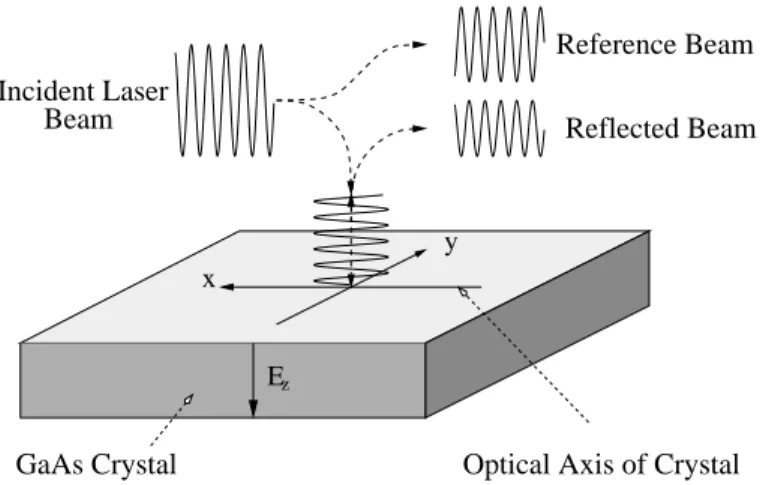
2.7.2 Internal probing
In the internal electro-optic probing of a GaAs chip the laser beam is focused onto the chip as dis-played in Figure 17. Considering that GaAs is transparent for infrared light, the infrared laser beam enters the chip, is modulated in the substrate and is reflected backwards.
The laser beam has to have certain properties in terms of wavelength, power and beam waist to make sure that the internal electro-optic sampling works well without systematic errors. A common setup for internal electro-optic probing is described in Figure 18. A continuous laser beam of a pigtailed Distributed FeedBack (DFB) laser is used as a laser source. First it passes a pigtailed optical circu-lator and it is focused on the chip with a system of lenses. An addition infrared camera displays the location and size of the laser beam spot on the chip. The reflected beam is recollected by the lens, reinjected into the optical fiber and passes again the optical circulator. After leaving the circulator by the port 3, the signal is optically amplified by an Erbium Doped Fiber Amplifier (EDFA) and filtered optically. Afterwards a fast photo detector converts the laser beam into an electric signal and a network analyzer is analyzing it.
There are several advantages of internal electro-optic probing. One is the fact, that an external elec-tro-optic crystal is not needed. So you do not have to place it just above the surface of your die and
Figure 15 Setup of a GaAs MMIC. Figure 16 Example of a standard MMIC.
GaAs Back Side (gold)
m 100 µ
Structure on Front side 10 µm
also there is no feedback from this crystal to your MMIC. Also the spatial resolution is better than with an external approach considering that the spot size of the laser beam is typically between
15[µm] and 30[µm]. The internal electro-optic probing is also the only approach where you can
measure the electric field inside the substrate. Another advantage is that the passivation of the chip does not have to be removed as the 0.15[µm]thick Si3N4passivation layer [ 39 ] is transparent for the laser beam.
On the other hand there are several disadvantages. You can only sample integrated devices based on a GaAs substrate. As the electro-optic effect of GaAs is rather weak the resulting signal is very small and as the laser beam has to enter the substrate, you cannot probe places hidden by wave guides.
2.8 Project for the thesis
The project of this Ph. D. thesis is to realize an internal probing tool for GaAs MMIC as well as to determine its theoretical and technical limits. The probing tool should be based on standard fiber equipment and standard microwave equipment. Hence the setup should be simple and “inexpensive” and should avoid the use of expensive and specially designed tools.
This thesis will continue previous work done in our laboratory. It is based on the results of the thesis of Quang-Dai Le [ 7 ] and Philipp Olivier Müller [ 8 ]. We will exploit the “basic ideas” of probing a Fabry Perot cavity with a continuous laser beam proposed in [ 7 ]. This approach has the advantage that we do not need a pulsed laser and we can avoid the difficulties with the synchronization between the microwave signal and the pulses of the probing beam. We will also use the proposition made in [ 8 ] regarding the use of standard fiber equipment and the calibration method for the probing of the absolute value of the electric field.
The original results of the presented work are the following parts: The previous works did always the assumption that the direction of the probed electric field is known e.g. parallel to the z-axis. As this assumption is not always true, we analyze the general case. We calculate the optical axis and refractive indices in function of the applied electric field and we determine the resulting modulation. The work presents the first electro-optic probing tool for MMIC using a pigtailed focuser. So we cal-culated the laser beam diameter and the divergence using the formalism of the Gaussian beam. An-other important part is the use of new equipment. As fiber optics did a lot a progress in the last time, this had a major impact on our probing tool. We start using Polarization Maintaining (PM) fibers, a pigtailed focuser and a powerful, tunable DFB laser.
Figure 17 Basic idea of internal electro-optic
sam-pling.
Figure 18 Setup proposed by [ 8 ] for internal
elec-tro-optic probing.
Laser beam Passivation
Semiconductor Electric field
Metal Layer
EDFA Optical Filter Photodiode Lens Polarizing beamsplitter Illumination IR Camera IR PM Fiber SM Fiber Isolator PM Fiber Analyser Network XY Table MMIC Temperature Controler Tunable DFB Circulator Optical
Theory
This chapter will explain the theory of electro-optic sampling using a Fabry Perot cavity. First we will have a look at the electro-optic effect in a crystal like Gallium Arsenide (GaAs). We will con-tinue with the calculation about the behavior of light in a Fabry Perot cavity. Afterwards we will combine both effects for the calculation of the modulation. At the end of the chapter, we will do some auxiliary considerations and comparisons.
Most of the following theory is based on the standard description of the electro-optic effect and the Fabry Perot cavity. The important part of the presented work is the description of our special con-figuration and its complete deduction. So we can find the origins of problems and explain them. Con-sidering that some of the mathematical calculations are rather long and complicated, the detailed deductions are placed in the appendix. So the reader can find the missing parts of the calculations.
3 Electro-Optic Effect
In vacuum or other isotropic materials, the propagation of an electro-magnetic wave does not depend on the direction of propagation or on its polarization. In such isotropic materials, the netic wave will always behave the same way. In crystals with periodic structures, the electro-mag-netic wave propagation will depend on the direction of the propagation as well as on the polarization of the wave. The properties of certain crystals can be changed by applying an external electric field. As these changes affect also a laser beam propagating inside the crystal, this type of crystal is called “electro-optic”.
3.1 General description of the problem
3.1.1 Isotropic and Anisotropic Material
In isotropic material the electric polarization of the material is always parallel to the applied
elec-tric field . So the dielectric susceptibilityχeis a scalar (Equation (7)).
(7)
By using and the relative dielectric constant we can show that the
elec-tric displacement is also parallel to the applied electric field (Equation (8)).
P E Px Py Pz ε0⋅χe Ex Ey Ez ⋅ = D = εoE+P εr= (1+χe) D
(8)
Under the condition that the crystal is not magnetic (µr=1) and that it is not absorbing (εrreal), it is easy to calculate the refractive index (Equation (9)) and hence the corresponding propagation veloc-ity of electro-magnetic waves.
(9)
For anisotropic material Equation (7) and (8) are not valid anymore because the material properties
of crystals depend on the crystal axis. So we have to replaceχeby a [3x3] matrix called the electric
susceptibility tensor (Equation (10)).
(10)
By applying we get the corresponding dielectric tensor (Equation (11)).
(11)
For the further calculations we assume that our crystal is homogenous (material properties are iden-tical for all points in the crystal), nonabsorbent (there is no energy loss in the crystal and soεxxare
real numbers) and that the material is not magnetic (µr=1). By using the Maxwell equation [ 11 ] we
can show that the dielectric tensor is symmetrical (Equation (12)) for these conditions.
(12)
For the following calculations, it is useful to define the impermeability tensor (Equation (13)).
or (13)
Sinceε is symmetrical its inverse matrixη is also.
3.1.2 Electro-Optic properties of Materials
In certain types of crystals, the application of an electric field causes a displacement of parts of the lattice and its charges. According to the quantum theory, the impermeability tensor depends on the distribution of the charges in the crystal. Mathematically we can describe this modification of the
impermeability tensor by a Taylor series in function of the applied electric field (Equation (14))
(14)
where is the impermeability tensor in the absence of an electric field, ri,j,k(a[3x3x3]matrix)
are the linear or Pockels1electro-optic coefficient. si,j,k,l([3x3x3x3] matrix) are the quadratic or
1. Effect discovered by the German physicist Friedrich Pockels around 1890.
Dx Dy Dz ε0 εr Ex Ey Ez ⋅ ⋅ = n = εr χ Px Py Pz ε0 χ11χ12 χ13 χ21χ22 χ23 χ31χ32χ33 Ex Ey Ez ⋅ ⋅ = ε = ε0(1+χ) ε Dx Dy Dz ε11ε12 ε13 ε21ε22 ε23 ε31ε32ε33 Ex Ey Ez ⋅ = εj i, = εi j, η η ε0 ε 1 – ⋅ = ε0⋅E = η⋅D η η( )E = η( )0 +ri j k, , ⋅E+si j k l, , , (E E⋅ ) …+ η( )0
Kerr1electro-optic coefficients. The magnitude of the electro-optic coefficient depends on the ma-terial as well as on its lattice. The higher order terms of Equation (14) are rather small so they can be neglected.
In our case we are interested in the electro-optic properties of GaAs. So we will examine its
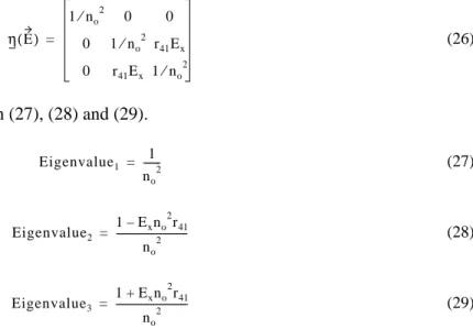
imper-meability tensor and the according material constant for this specific material. For GaAs is
represented by Equation (15). We can see that Equation (15) satisfies the condition of Equation (12). Hence in the absence of an applied electric field, GaAs is isotropic because the electric field vector and the electric displacement vector are always parallel.
(15)
In Equation (16) we have the linear electro-optic coefficient of GaAs written as a[3x3x3]matrix as
well as the applied electric field given in Cartesian coordinates.
and (16)
The symmetry in Equation (16) imposed by the condition of Equation (12), limits the number of in-dependent coefficients in the impermeability tensor ([3x3] matrix) to six. Very often this fact is used to reduce Equation (16) into a [6x3] matrix like Equation (17), easier to represent on a two-dimen-sional sheet of paper. So each of the six independent coefficient depends on Ex, Ey as well as Ez.
(17)
By using Table 1, you can convert the [3x3x3] matrix of Equation (16) into the [6x3] matrix of Equation (17).
1. Effect discovered by the english physicist John Kerr around 1875.
η( )0 η( )0 1 n0 2 ⁄ 0 0 0 1 n0 2 ⁄ 0 0 0 1 n0 2 ⁄ = ri j k, , 0 0 0 0 0 r41 0 r41 0 0 0 r41 0 0 0 r41 0 0 0 r410 r41 0 0 0 0 0 , , = E Ex Ey Ez = rI k, 0 0 0 0 0 0 0 0 0 r41 0 0 0 r41 0 0 0 r41 =
Table 1 Lockup table for the index I that represents the pair of indices (i,j) [ 1 ].
So for the element r(i=3,j=2,k=1) you will have to take element rI,k(4,1)=r41.
i = 1 i = 2 i = 3
j = 1 1 6 5
j = 2 6 2 4
In GaAs the Kerr effect is very weak or with other words, we can neglect the quadratic electro-optic coefficients. So we can describe the impermeability tensor of GaAs for an applied electric field by Equation (18).
(18)
It is important to notice that this tensor defines the propagation of an electro-magnetic wave in the crystal. So this mechanism affects the laser beam as well as a microwave signal traveling across the crystal.
In the further deductions, we are interested in the propagation of laser beam with a frequency of
1. So for the refractive index n
o, we have to take according
to [ 3 ].
For the electro-optic coefficient r41the choice becomes more delicate as the coefficient depends on
νLaseras well as on the frequency of the applied electric field . In our case the frequency
is in the range of 0.1 to 20
[
GHz]
. Hence we can use the electro-optic coefficientas proposed in [ 8 ].
We have to point out that for much higher frequencies thanνMicrowave, the electro-optic coefficient
r41(ν) becomes negligible. The basic physical concepts of this behavior are understood [ 12 ], but
there are no reliable publications on the cut-off frequency of the electro-optic coefficient for GaAs.
This “phenomenon” forbids the influence of the electric field of the laser beam on and so the
laser beam is modulated by the microwave signal and not vice versa.
3.1.3 Principle of the Ellipsoid
In the previous paragraph we discussed the electro-optic effect and the modification of the imperme-ability tensor by an applied microwave signal. For the ‘every day calculations’ the use of the imper-meability tensor or the dielectric tensor is too complicated.
The method to simplify the application of the impermeability tensor is to use the eigenvectors and the eigenvalues of the tensor in Equation (18). The resulting vector of the multiplication of the ma-trix with its eigenvector is parallel to the original eigenvector as explained in Equation (19). The ab-solute value of the eigenvector has to be multiplied with its eigenvalue to get the abab-solute value of resulting vector.
(19)
A symmetrical [3x3] matrix has three eigenvalues and three according eigenvectors. With linear al-gebra, we can prove that the three eigenvectors for a symmetrical matrix are three orthogonal vec-tors. Also we can demonstrate that the eigenvectors of a matrix and the eigenvectors of its inverse matrix are identical.
So the eigenvectors of the impermeability tensor are identical with the eigenvectors of the dielectric
1. Corresponds to a wavelength of 1550[nm]or a photon energy of 0.80[eV].
E η( )E 1 n0 2 ⁄ r41Ez r41Ey r41Ez 1 n0 2 ⁄ r41Ex r41Ey r41Ex 1 n0 2 ⁄ = νLaser≈193 THz[ ] no(νLaser)= 3.374 νMicrowave E νMicrowave r41(νMicrowave) 1.4 10 12 – m V⁄ [ ] ⋅ = η( )E M11M12 M13 M21M22 M23 M31M32 M33 Eigenvectorx Eigenvectory Eigenvectorz ⋅ Eigenvalue Eigenvectorx Eigenvectory Eigenvectorz ⋅ =
tensor. Hence for the direction of the eigenvectors, the electric field is parallel to the electric dis-placement and the corresponding electric polarization. So for this direction of the electric field, the electro-magnetic wave is propagating like in isotropic material with a dielectric constant correspond-ing to the eigenvalues of the dielectric tensor. For optical applications the direction of the eigenvec-tors are called the ‘optical axes’ of the material.
The Maxwell’s equations are linear so long as the wave power is not strong enough to significantly perturb the material. So the propagation for the other orientation of the electric field can be described by projecting the electric field vector on the three eigenvectors and by calculating the propagation for each component separately (Figure 19).
By using the results of Appendix E.1. on page 115, we find the eigenvalues ξ1,2,3 given in
Equation (20) to (22) for the impermeability tensor of Equation (18).
(20)
(21)
(22)
In these equations Ex, Ey and Ez are the x, y and z component of the applied electric field,
is the magnitude of the electric field, r41 is the electro-optic coefficient of
GaAs and no is the refractive index in the absence of an (microwave) electric field.
By using the results of Appendix E.2. on page 116 the corresponding non-normalized eigenvectors are given by Equation (23) to (25). So we can see that the eigenvalues of the impermeability tensor
depend on the electro-optic coefficient r41as well as on the amplitude of the applied electric field
and its direction. As the refractive index of the material is a function of the eigenvalues, it will also depend on these parameters. On the other hand the eigenvectors (which are parallel with the optical axis of the material) depend only on the directions of the electric field.
Figure 19 Projection of the electric field vector on the
eigen-vectors of the material.
Projection on Optical Axis Optical Axis =
Eigenvectors
Crystal Electric field vector
ξ1 1 no 2 --- 2 3 --- E arc 3 3ExEyEz E3 ---– cos 3 --- cos r41 ⋅ ⋅ + = ξ2 1 no 2 --- 2 3 --- E π 3 ---arc 3 3ExEyEz E3 ---– cos 3 ---– r41 ⋅ cos ⋅ – = ξ3 1 no 2 --- 2 3 --- E π 3 ---arc 3 3ExEyEz E3 ---– cos 3 ---+ r41 ⋅ cos ⋅ – = E Ex 2 Ey 2 Ez 2 + + =
with (23) with (24) with (25)
3.1.4 Representation as an ellipsoid
For the visualization and for the application of the results, we use an ellipsoid. The three eigenvectors define the direction of three axis of the ellipsoid and the eigenvalues indicate the magnitudes of the axes (Figure 20

![Figure 31 Amplitude and phase shift of the electro-optic signal. For this figure we used the following parameters: n o =3.374, r 41 =1.42 10 -12 [ m/V ] , r=0.54, R=0.63 (-2 [dB]), d=500 [µm], E Microwave =1 [V]/d [m] and P Incident =1 [mW].](https://thumb-eu.123doks.com/thumbv2/123doknet/11439099.289989/46.892.308.634.146.465/figure-amplitude-electro-signal-following-parameters-microwave-incident.webp)
![Figure 35 Amplitude at the output of the analyzer. For this figure we used the following parameters: n o =3.374, r 41 =1.42 10 -12 [m/V], r=0.54, R=0.63 (-2 [dB]), d=500 [µ m ] , E Microwave =1 [ V ]/ d [ m ] and P Incident =1 [ mW ] .](https://thumb-eu.123doks.com/thumbv2/123doknet/11439099.289989/51.892.225.620.503.761/figure-amplitude-output-analyzer-following-parameters-microwave-incident.webp)
![Figure 38 Amplitude of the output of the phase modulations. For this figure we used the following param- param-eters: n o =3.374, r 41 =1.42 10 -12 [m/V], r=0.54, R=0.63 (-2 [dB]), d=500 [µm], E Microwave =1 [V] / d [m]](https://thumb-eu.123doks.com/thumbv2/123doknet/11439099.289989/55.892.121.740.121.298/figure-amplitude-output-phase-modulations-figure-following-microwave.webp)

![Figure 51 Fabry Perot response with addition loss. The used parameters are r + =0.37, R + =0.29, d=500 [ µ m], P Incident =1 [mW], n GaAs =3.374, a phase shift of Λ=π/4 and P Incident =1 [mW]..](https://thumb-eu.123doks.com/thumbv2/123doknet/11439099.289989/65.892.229.614.312.578/figure-fabry-perot-response-addition-parameters-incident-incident.webp)

![Table 4 Characteristics of the circulator used for the setup for λ o =1550 [nm].](https://thumb-eu.123doks.com/thumbv2/123doknet/11439099.289989/74.892.256.689.474.706/table-characteristics-circulator-used-setup-λ-o-nm.webp)
