Pépite | Transmetteurs radiofréquences numériques fortement parallélisés avec amplificateur de puissance commuté et filtre de bande embarqués en technologie 28nm FD-SOI CMOS
197
0
0
Texte intégral
(2) Thèse de Răzvan-Cristian Marin, Lille 1, 2017. Abstract The present PhD work covers the study, design and demonstration of all-digital. transmitters targeting advanced communication standards for mobile applications in the frame of the Internet of Things (IoT). Key innovations are time-interleaved Delta-Sigma. modulators (DSM) and a power and area-efficient switched-capacitor (SC) finite impulse response power amplifier (FIR-PA).. The proposed transmitter architecture comprises a single-bit 8-channel time-. interleaved (TI) DSM, which enables a simplified operation of the output stage with a. double function of power amplifier and FIR filter. The common FIR-PA block uses exclusively inverters and capacitors in a switched-capacitor configuration, thus being fully. compatible with advanced CMOS technology nodes. A particular attention is paid to the complexity and power consumption of the output stage by reducing switching redundancy. and co-designing the band filter together with an output RLC filter.. The prototype is integrated in 28nm FD‐SOI CMOS technology with 10 metal layers. and body biasing fine-tuning features. The integrated circuit (IC) is packaged in a custom Ball-Grid Array (BGA) package, including additional passive components. The proposed digital RF transmitter based on 1‐bit delta-sigma modulators and switched-capacitor. power amplifier with embedded 109‐tap FIR band filter achieves 13.5 in‐band effective number of bits (ENOB) and is 900 MHz LTE‐compliant.. The overall power consumption is 35 mW at 2.9 dBm peak output power and 1V. supply. LO and image rejection are >55 dBc thanks to FD‐SOI body‐bias Vt fine-tuning. With respect to relevant state-of-the art, at similar output power levels, the FIR‐PA (at 1 V). consumes 7 times less than a 10‐bit DSM‐based DAC (at 1.5 V) and 25% less than a 12‐bit. Marin Răzvan-Cristian, PhD Thesis 2017. Page i.
(3) Thèse de Răzvan-Cristian Marin, Lille 1, 2017. resistive DAC (at 0.9 V). The total active area is 0.047 mm2, at least 4 times lower than the smallest previously published work.. Consequently, this work stands out for low power consumption thanks to the single-. bit core solution combined with band filtering and low area achieved with a multi-layer FIR-PA cell structure. It demonstrates the transition from traditional analog to highly integrated digital-intensive transmitters targeting the future of mobile applications.. Keywords: Delta-sigma modulation (DSM), Time-interleaving (TI), Finite impulse. response filter (FIR), Switched-capacitor (SC) power amplifier (PA), FIR-PA, 28nm FD-SOI,. Body-bias, Vt fine-tuning, All-digital transmitter.. Abstract. Page ii.
(4) Thèse de Răzvan-Cristian Marin, Lille 1, 2017. Résumé Le présent travail de thèse porte sur l’étude, la conception et la démonstration. d'émetteurs entièrement numériques, ciblant des standards de communication avancés pour les applications mobiles dans le cadre de l’Internet des Objets (IoT). Les innovations clés sont le modulateur Delta-Sigma (DSM) entrelacé et un amplificateur de puissance à. réponse impulsionnelle finie (FIR-PA) basé sur une structure efficace à capacités commutées (SC).. L'architecture d’émetteur proposée comprend un DSM entrelacé (TI) à 8 canaux qui. permet un fonctionnement simplifié de l'étage de sortie avec une double fonction. d'amplificateur de puissance et de filtre FIR. Le block FIR-PA utilise uniquement des. inverseurs CMOS et des condensateurs dans une configuration SC, ce qui est entièrement. compatible avec les nœuds technologiques CMOS avancés. Une attention particulière est. accordée à la complexité et à la consommation d'énergie de l’étage de sortie, en réduisant la. redondance de commutation et en réalisant un co-design du filtre de bande avec un filtre RLC en sortie.. Le prototype est implémenté dans une technologie 28nm FD-SOI CMOS avec 10. couches métalliques et un contrôle amélioré de la tension du substrat. Le circuit intégré. (IC) est monté dans un substrat de type BGA, avec des composants passifs supplémentaires. L'émetteur RF numérique basé sur les modulateurs delta-sigma 1-bit et l'amplificateur de. puissance à capacités commutées, intégrant un filtre de bande avec 109 coefficients, atteint un nombre de bits effectif (ENOB) de 13.5 dans la bande de signal utile et est compatible avec le standard LTE 900 MHz.. Marin Răzvan-Cristian, PhD Thesis 2017. Page iii.
(5) Thèse de Răzvan-Cristian Marin, Lille 1, 2017. Le circuit consomme 35 mW à une puissance de sortie maximale de 2.9 dBm et une. alimentation de 1 V. La rejection des composants de l’oscillateur local (LO) et d'image est > 55 dBc, grâce au réglage fin du Vt par polarisation du substrat. Par rapport à l'état de l'art,. à des niveaux de puissance de sortie similaires, le FIR-PA (à 1 V) consomme 7 fois moins. qu'un DAC 10-bit intégrant des modulateurs delta-sigma (à 1.5 V) et 25% moins qu’un DAC. résistif 12-bit (à 0.9 V). La surface active totale est de 0.047 mm2, soit 4 fois moins que le plus petit circuit publié précédemment.. Par conséquent, ce travail se distingue par une faible consommation d'énergie grâce à. la l’architecture 1-bit combinée au filtrage de bande et par la surface réduite obtenue par. l’intégration efficace des cellules du FIR-PA. Il démontre la transition de l’émetteur. analogique traditionnel à l’émetteur numérique intégré ciblant l'avenir des applications mobiles.. Mots-clés : Modulation delta-sigma (DSM), Entrelacement temporel (TI), Filtre à. réponse impulsionnelle finie (FIR), Amplificateur de puissance (PA) à capacités commutées (SC), FIR-PA, 28nm FD-SOI, Polarisation du substrat (Body-Bias), Réglage fin du Vt,. Émetteur numérique.. Résumé. Page iv.
(6) Thèse de Răzvan-Cristian Marin, Lille 1, 2017. List of publications [Marin15] R.-C. Marin, A. Frappé, A. Kaiser, and A. Cathelin, “Considerations for high-speed configurable-bandwidth time-interleaved digital delta-sigma modulators and synthesis in. 28 nm UTBB FD-SOI,” in 2015 IEEE 13th International New Circuits and Systems Conference (NEWCAS), Grenoble, pp. 1–4, June 2015.. This paper presents the design and simulation of a time-interleaved delta-sigma. modulator as part of a digital transmitter chain. The architecture is chosen based on a critical path analysis in order to reach very high frequency operation. The modulator’s configurability allows it to target signal bandwidths from 20 MHz up to 160 MHz with a SNR greater than 67 dB. Finally, the modulator is synthesized using standard cells in 28nm FDSOI CMOS from STMicroelectronics and simulated for different numbers of time-interleaved channels, reaching a sample rate of up to 6 GS/s. An optimum number of channels can be found based on a trade-off between operating frequency, supply voltage, power consumption and area.. [Marin16] R.-C. Marin, A. Frappé, A. Kaiser, “Delta-Sigma Based Digital Transmitters with. Low-Complexity Embedded-FIR Digital to RF Mixing,” 23rd IEEE International Conference on Electronics, Circuits and Systems (ICECS), Monte Carlo, pp. 237-240, Dec. 2016.. The focus of this contribution is to review delta-sigma based all-digital transmitters and. to discuss issues related to large out-of-band quantization noise and possible coexistence problems. Low-complexity embedded-FIR filters are very interesting to relax the filtering constraints while keeping systems as digital as possible to benefit from the advanced CMOS node integration. In this paper we propose a single-bit digital to RF mixer with embedded-FIR, which provides noise level reduction at specific frequencies in order to target multi-standard coexistence. This architecture introduces simple logic operating at low frequency which enables single-bit output and avoids the use of an additional delayed DAC, thus reducing. Marin Răzvan-Cristian, PhD Thesis 2017. Page v.
(7) Thèse de Răzvan-Cristian Marin, Lille 1, 2017. considerably the power consumption and area of the output stage. Finally, we introduce an asymmetric unbalanced FIR architecture to provide a complementary solution for out-of-band noise reduction.. [Marin17a] R.-C. Marin, A. Frappé, A. Kaiser, “Considerations for Complex Digital DeltaSigma Modulators for Standard Coexistence in Digital Wireless Transmitters,” accepted to. IEEE Trans. Circuits Syst. I, Reg. Papers, June 2017.. This paper presents a Complex Delta-Sigma Modulator (CDSM) designed for integration. in a digital transmitter chain targeting multi-standard coexistence with nearby receivers. A review of known design methods for CDSM revealed limitations regarding the poles/zeros optimization, and the configurability of the complex zeros placement. The proposed architecture introduces two additional cross-couplings from the I and Q quantizers outputs in order to decorrelate the zeros placement and the poles optimization problem. Hence, the improved CDSM can be implemented using existing optimization tools, which reduces considerably the number of iterations and the computational effort. In addition, the resulting modulator can target different coexistence scenarios without the need of redesign, unlike other known methods. Simulation results show a noise level reduction of approximately 2030 dB near specific frequency bands by the proposed CDSM scheme with respect to standard DSM. Finally, we show an efficient coarse/fine configurability mechanism, which is obtained when introducing additional delays in the cross-coupling paths.. [Marin17b] R.-C. Marin, A. Frappé, B. Stefanelli, P. Cathelin, A. Cathelin, A. Kaiser, “A 28nm FD-SOI CMOS Digital RF Transmitter with Switched-Capacitor Pre-Power Amplifier and Embedded Band Filter,” to be submitted to Journal of Solid-State Circuits.. This paper introduces a 900MHz LTE‐compliant digital RF TX based on 1‐bit ΔΣM and. SC pre‐PA with embedded 109‐tap FIR (FIR‐PPA) Band Filter achieving 13.5 in‐band ENOB. The FIR‐PPA is built with CMOS inverters and Metal‐Oxide‐Metal capacitors, integrated directly under flip‐chip RF pads in 28nm FD‐SOI CMOS. The overall power consumption is 35mW at 2.9dBm peak output power and 1V supply. LO and image rejection are >55dBc thanks to FD‐SOI body‐bias Vt tuning. The total active area is 0.047mm2.. List of publications. Page vi.
(8) Thèse de Răzvan-Cristian Marin, Lille 1, 2017. Acknowledgments It was a real adventure, having alongside great people to whom I wish to extend my. deepest gratitude. I will always cherish these moments.. Andreas, your always challenging comments, questions, remarks have added a great. value to this work. It was a pleasure working with you on defining and expressing clear concepts and ideas, and learning from one of the best.. Andreia and Philippe, your excellent guidance allowed a perfect combination of. theory and practice, academia and industry, to explore the full circuit design flow from idea. to prototype and see the “bigger picture”. Thank you for the access to high-end technology and the opportunity to discover and work briefly at STMicroelectronics, which were definitive in reaching my goals.. Antoine, thank you for your full support throughout this period and the “always open-. door” policy. Thank you for the passionate discussions, brain-storming and idea definition, it was an exciting ride, and you were there all the way.. Nathalie Deltimple, Jussi Ryynänen, Henrik Sjöland and Cristophe Loyez, thank you. for accepting the invitation to report and examine my work and I’m looking forward to your future comments, questions, remarks which represent an excellent opportunity for improvement.. I wish to thank the Hauts-de-France Region (formerly Nord-Pas-de-Calais) and. STMicroelectronics for funding this PhD work through CNRS. Also, I wish to thank the. Research Council of the Catholic University of Lille, for research funding and rewarding me with the 2nd prize in the PhD Research Contest 2016. Marin Răzvan-Cristian, PhD Thesis 2017. Page vii.
(9) Thèse de Răzvan-Cristian Marin, Lille 1, 2017. Bruno Stefanelli, your involvement, availability, attention to details and design. experience, were indispensable in the success of this work.. Axel Flament, thank you for taking the time to pass some of your experience,. especially for transmission line design.. Jean-Marc Capron, thank you for your involvement in the project, raising questions,. and clarifying key-points. In addition, thank you for giving me the opportunity to teach at. ISEN, it was a great experience which helped me gain confidence in public speech and develop social skills.. Cristophe Denoyelle, thank you for mastering fine BGA soldering which allowed fast. measurement setup and debug, in order to obtain the best possible performance. Your availability and curiosity played a defining role.. Emmanuel Dubois, thank you for the institutional and experimental support at IEMN. and ISEN.. Rédha Kassi and Laurent Bigot, thank you for the access to measurement equipment. and setup support at IRCICA.. To Didier Campos and the packaging integration team at STMicroelectronics, special. thanks for the BGA design, packaging and follow-up on measurements.. Florence Alberti, thank you for your availability, help and prompt solution to any. administrative situation.. Nora Benbahlouli, thank you for the administrative support at IEMN.. Anne-Marie, thank you for your support in entering the PhD research contest, for. your kindness and for the occasional discussions on everything and anything which usually started in French and finished in Romanian.. Evelyne Litton, thank you for welcoming me wholeheartedly at ISEN 4 years ago and. for your warm and friendly attitude. The same goes for the entire SMART department at. ISEN. This made the adjustment to France and Lille very smooth, thank you for your hospitality.. Acknowledgments. Page viii.
(10) Thèse de Răzvan-Cristian Marin, Lille 1, 2017. I would also like to thank fellow PhD, PostDoc past and present for their advice,. company and friendship. Hani, thank you for sharing some of your knowledge and. experience during my stay at ST, and for a comforting word in a sorrow day. Reda and Nassim, thank you for interesting discussions on chip integration and providing a friendly. environment at ST. Camillo and Matteo, you guys spent too little time at ISEN and you. were/are definitely missed, I wish you all the best. Ilias, you brought a mix of maturity and cheerful attitude to the group, thank you for your advices both professionally and. personally. Fikre, thank you for providing a calm, friendly working environment in office, during TP or at conferences. Now, the senior PhD role is passed to Dipal, always cheerful,. you are great, just “keep calm and tape-out” (as Ilias used to say). Greetings to Angel, you are on the right path.. Miruna Nițescu and Florin Constantinescu, thank you for your guidance during. Bachelor and Master studies, for the important role you played in the opportunity to study. in France, and generally for being there and supporting me both professionally and. personally.. Cornel Stănescu, thank you for giving me the opportunity to explore industry analog. IC design at a high-level, and inspiring the desire to go further on towards PhD.. Finally, I wish to thank my family, my mom and dad for everything they did for me,. love, cherish, sacrifices, the possibility to go and pursue my dreams via the best investment. -in education-, my brother, my best friend, always supportive, listening and advising,. Typhaine for her love and indefinite support, Valérie and Denis for their warmth, hospitality, trust and consideration.. Marin Răzvan-Cristian, PhD Thesis 2017. Page ix.
(11) Thèse de Răzvan-Cristian Marin, Lille 1, 2017. Acknowledgments. Page x.
(12) Thèse de Răzvan-Cristian Marin, Lille 1, 2017. Table of contents Abstract........................................................................................................................................... i Résumé .......................................................................................................................................... iii List of publications........................................................................................................................ v Acknowledgements ..................................................................................................................... vii Table of contents .......................................................................................................................... xi List of figures ............................................................................................................................. xvii List of tables.............................................................................................................................. xxiii List of acronyms ........................................................................................................................ xxv Chapter 1. Introduction................................................................................................................ 3 1.1. Motivation .......................................................................................................................... 3 1.2. Research considerations ..................................................................................................... 4 1.3. Main contributions ............................................................................................................. 6 1.4. Manuscript organization .................................................................................................... 7 1.5. Chapter Bibliography ......................................................................................................... 8. Marin Răzvan-Cristian, PhD Thesis 2017. Page xi.
(13) Thèse de Răzvan-Cristian Marin, Lille 1, 2017. Chapter 2. WLAN Transmitters ............................................................................................... 11 2.1. IEEE 802.11 Standard Specifications .............................................................................. 11 2.1.1. Channelization ..................................................................................................... 13 2.1.2. Transmit Spectral Mask ....................................................................................... 15 2.1.3. Transmitter Measurements................................................................................... 16 2.2. State-of-the-art in wireless transmitter architectures ....................................................... 16 2.2.1. Analog transmitters .............................................................................................. 16 2.2.2. Digital Transmitters ............................................................................................. 20 2.2.2.1. Polar architecture........................................................................................ 21 2.2.2.2. Cartesian architecture ................................................................................. 25 2.3. Conclusion ....................................................................................................................... 27 2.4. Chapter Bibliography ....................................................................................................... 30 Chapter 3. Transmitter architecture description .................................................................... 33 3.1. Introduction ...................................................................................................................... 33 3.2. Digital Delta-Sigma Modulators ...................................................................................... 37 3.2.1. Basic concepts...................................................................................................... 38 3.2.1.1. Quantization Noise ..................................................................................... 39 3.2.1.2. Oversampling ............................................................................................. 39 3.2.1.3. 1st order noise shaping ................................................................................ 40 3.2.1.4. Higher-order noise shaping ........................................................................ 41 3.2.2. Increased effective operating frequency .............................................................. 43 3.2.2.1. Time-interleaving methods ........................................................................ 45 3.2.2.2. Critical path study ...................................................................................... 47 3.2.3. CIFB architecture ................................................................................................. 48 3.2.3.1. CIFB DSM design specifications ............................................................... 48 3.2.3.2. Architecture coefficients ............................................................................ 49 3.2.4. DSM synthesis ..................................................................................................... 51 Table of contents. Page xii.
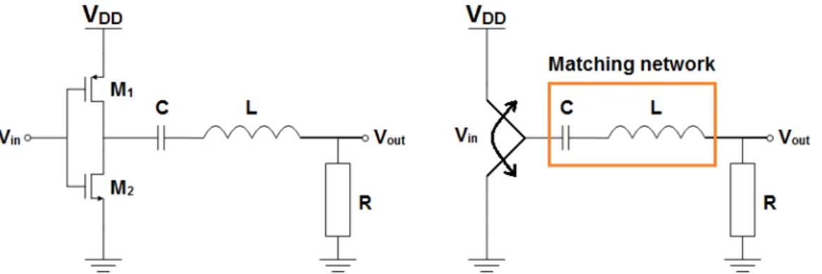
(14) Thèse de Răzvan-Cristian Marin, Lille 1, 2017. 3.3. FIR-PA ............................................................................................................................. 52 3.3.1. FIR Filter.............................................................................................................. 52 3.3.2. Power amplifier .................................................................................................... 54 3.3.2.1. Design specifications.................................................................................. 56 3.3.2.2. Filter optimization using the matching network ........................................ 56 3.3.3. Efficiency ............................................................................................................. 60 3.3.3.1. Single-ended FIR-PA efficiency ................................................................ 64 3.3.3.2. Differential FIR-PA efficiency................................................................... 67 3.3.3.2.1. Optimization of the switching activity ................................................ 67 3.3.3.2.2. Half-SC FIR-PA .................................................................................. 68 3.3.3.2.3. Comparison with ideal high-resolution DAC...................................... 72 3.4. FIR-PA non-idealities ...................................................................................................... 73 3.4.1. Non-ideal switch model ....................................................................................... 74 3.4.1.1. Power spectral density estimation .............................................................. 76 3.4.1.2. Model of the rise/fall time .......................................................................... 78 3.4.1.3. Model of the low-to-high/high-to-low delay .............................................. 79 3.4.1.4. Combined model of rise/fall time, LH/HL delay and jitter ........................ 80 3.4.1.5. Results ........................................................................................................ 82 3.4.2. Non-ideal FIR filter coefficients .......................................................................... 85 3.4.2.1. Estimation................................................................................................... 85 3.4.2.2. Comparison with non-ideal high-resolution DAC ..................................... 87 3.4.2.3. Compensation ............................................................................................. 88 3.5. Voltage supply variation .................................................................................................. 89 3.6. Conclusion ....................................................................................................................... 91 3.7. Chapter Bibliography ....................................................................................................... 93. Marin Răzvan-Cristian, PhD Thesis 2017. Page xiii.
(15) Thèse de Răzvan-Cristian Marin, Lille 1, 2017. Chapter 4. All-digital transmitter circuit design ..................................................................... 97 4.1. Transmitter IC description ............................................................................................... 97 4.1.1. IC block diagram.................................................................................................. 98 4.1.2. IC configuration and physical implementation .................................................... 99 4.2. Switched-capacitor FIR-PA design................................................................................ 102 4.2.1. Configurable FIR-PA ......................................................................................... 102 4.2.1.1. Initial estimation of power cell distribution ............................................. 103 4.2.1.2. Actual power cell distribution .................................................................. 104 4.2.2. Unitary power cell.............................................................................................. 106 4.2.2.1. CMOS inverter design .............................................................................. 107 4.2.2.1.1. Inverter sizing .................................................................................... 108 4.2.2.1.2. MOM capacitor design ...................................................................... 109 4.2.2.1.3. Power consumption estimation ......................................................... 111 4.2.2.1.4. Effect of the CMOS inverter on-resistance ....................................... 113 4.2.2.2. FIR-PA cells overview ............................................................................. 113 4.2.2.3. Decoupling capacitors .............................................................................. 114 4.2.2.4. Power efficiency estimation ..................................................................... 116 4.2.3. FIR-PA structure ................................................................................................ 119 4.2.3.1. Ideal PA performance............................................................................... 120 4.2.3.2. Layout parasitic extraction ....................................................................... 120 4.3. Digital block design ....................................................................................................... 124 4.3.1. Input signals generation ..................................................................................... 124 4.3.2. FIR-PA SIGGEN block ..................................................................................... 128 4.3.3. Digital to RF mixer ............................................................................................ 130 4.3.4. Power consumption estimation .......................................................................... 131 4.4. Conclusion ..................................................................................................................... 132 Table of contents. Page xiv.
(16) Thèse de Răzvan-Cristian Marin, Lille 1, 2017. 4.5. Chapter Bibliography ..................................................................................................... 136 Chapter 5. Measurements ........................................................................................................ 139 5.1. IC Packaging .................................................................................................................. 139 5.2. PCB design..................................................................................................................... 140 5.2.1. High-speed signal line design ............................................................................ 141 5.2.2. RF differential outputs ....................................................................................... 142 5.3. Measurement setup and test cases.................................................................................. 144 5.3.1. Case 1: Functional.............................................................................................. 145 5.3.2. Case 2: FIR filter with transmission line adaptation.......................................... 147 5.3.3. Case 3: Higher frequency operation .................................................................. 149 5.4. Experimental IC validation on LTE standard at 900 MHz band ................................... 150 5.5. Conclusion ..................................................................................................................... 154 5.6. Chapter Bibliography ..................................................................................................... 156 Chapter 6. Conclusion .............................................................................................................. 157 6.1. Research conclusion....................................................................................................... 157 6.2. Future directions ............................................................................................................ 158 6.3. Chapter Bibliography ..................................................................................................... 161 Additional work. Multi-standard coexistence ........................................................................ 163 A.1. Complex Delta-Sigma Modulators ............................................................................... 163 A.2. Embedded-FIR digital to RF mixing ............................................................................ 166 A.3. Chapter Bibliography .................................................................................................... 168. Marin Răzvan-Cristian, PhD Thesis 2017. Page xv.
(17) Thèse de Răzvan-Cristian Marin, Lille 1, 2017. Table of contents. Page xvi.
(18) Thèse de Răzvan-Cristian Marin, Lille 1, 2017. List of figures Chapter 1 Fig. 1.1. Battery - smartphone ........................................................................................................ 3. Chapter 2 Fig. 2.1. Overview of overlapping channels in 2.4 GHz band [Tektronix13] .............................. 12 Fig. 2.2. Overview of non-overlapping channels in 2.4 GHz band [Tektronix13] ....................... 13 Fig. 2.3. Available non-overlapping channels in 5 GHz band [Cisco13] ..................................... 13 Fig. 2.5. OFDM spectral mask for 802.11a/g/n/ac [Tektronix13] ................................................ 14 Fig. 2.6. Traditional analog transmitter architecture..................................................................... 16 Fig. 2.7. Transmitter block diagram with mixer-PA interface [Kumar13] ................................... 17 Fig. 2.8. Block diagram of the dual-band 3-stream MIMO WLAN radio [He14] ....................... 17 Fig. 2.9. Transmitter block diagram [Chen14] ............................................................................. 18 Fig. 2.10. General representation of a data point .......................................................................... 20 Fig. 2.11. Polar representation bandwidth expansion ................................................................... 21 Fig. 2.12. Digital Polar transmitter block diagram [Zheng13] ..................................................... 21 Fig. 2.13. Proposed outphasing TX architecture [Ravi12] ........................................................... 22 Fig. 2.14. Digitally modulated polar TX: Architecture (a); Drain efficiency (b) [Ye13] ............. 23 Fig. 2.15. Class-G SC PA: Architecture (left); Ideal efficiency (right) [Yoo13] ......................... 23 Fig. 2.16. Spectrum Cartesian representation ............................................................................... 24 Fig. 2.17. TX block diagram (left); QAM spectrum including replicas (right) [Alavi14] ........... 24 Fig. 2.18. All-digital quadrature transmitter architecture [Wang14] ............................................ 25 Fig. 2.19. Digital PWM transmitter system level view [Hezar14] ............................................... 26. Marin Răzvan-Cristian, PhD Thesis 2017. Page xvii.
(19) Thèse de Răzvan-Cristian Marin, Lille 1, 2017. Chapter 3 Fig. 3.1. Traditional Analog Transmitter (left); Digital Transmitter (right) ................................. 32 Fig. 3.2. Digital I/Q modulation block diagram [Alavi14] ........................................................... 33 Fig. 3.3. D-RF architecture based on single-bit DSM [Frappe09]................................................ 33 Fig. 3.4. Digital TX: Image replicas [Alavi14] (left); Out-of-band noise [Frappe09] (right) ...... 34 Fig. 3.5. FIR-DAC [Gebreyohannes16]: TX block diagram (a); 1-bit N-length FIR DAC (b).... 35 Fig. 3.6. Proposed concept of all-digital transmitter with embedded-FIR PA ............................. 36 Fig. 3.7. Delta-Sigma Modulation concept ................................................................................... 37 Fig. 3.8. Quantizer (left) and its linear model (right) [Kozak03] ................................................. 38 Fig. 3.9. 1st order DSM architecture ............................................................................................. 39 Fig. 3.10. Discrete-time integrator (left) and resonator (right) ..................................................... 40 Fig. 3.11. 3rd order CIFB architecture ........................................................................................... 41 Fig. 3.12. MASH 1-1 architecture ................................................................................................ 42 Fig. 3.13. Pipelining using 5-bit and 6-bit ripple carry adders (RCA5/RCA6) [Schmidt11] ....... 43 Fig. 3.14. Equivalent block filtering structure for SISO transfer function H(z) [KP93] .............. 44 Fig. 3.15. 1st order 2-channel TI DSM: poly-phase (left); node equations (right) [Marin15] ...... 46 Fig. 3.16. 3rd order CIFB architecture with 1-bit bandwidth control [Marin15] .......................... 48 Fig. 3.17. NTF of the 3rd order CIFB DSM: g1 = 0; g1 = 2-7 [Marin15] ....................................... 49 Fig. 3.18. TI DSM estimated maximum operating frequency ...................................................... 50 Fig. 3.19. 1-bit DSM output spectrum (Amplitude scaled to Pout = 20 dBm, BW = 20 MHz) ..... 52 Fig. 3.20. Simulated output spectrum: FIR filtered DSM output (BW = 20 MHz) ...................... 53 Fig. 3.21. Switching-mode class-D PA: active devices (left); ideal switch (right) ...................... 54 Fig. 3.22. Switching-mode class-D PA with embedded N-length FIR filter ................................ 54 Fig. 3.23. Transfer function 2nd order BPF filter : {R, L, C}, {2*R, L, C}, and {R, 2*L, C/2} .. 56 Fig. 3.24. Simulated output spectrum: FIR 5-bit and RLC vs. FIR 8-bit (BW = 20 MHz) .......... 58 Fig. 3.25. Digital Cartesian transmitter based on single-ended FIR-PA ...................................... 60 Fig. 3.26. 2-bit SC PA: at t0 (left) and t1 (right) ............................................................................ 61 Fig. 3.27. Schematic of an ideal unitary power cell in Cadence ................................................... 63 Fig. 3.28. ISI with asymmetric fronts (a); resulting output spectra (b) [Frappe07] ...................... 65 Fig. 3.29. FIR-PA differential architecture ................................................................................... 66 Fig. 3.30. Half-SC FIR-PA differential architecture..................................................................... 68 List of figures. Page xviii.
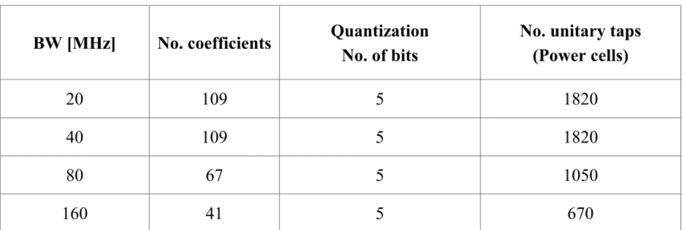
(20) Thèse de Răzvan-Cristian Marin, Lille 1, 2017. Fig. 3.31. Power efficiency characteristics ................................................................................... 70 Fig. 3.32. Output spectrum: comparison Half-SC FIR-PA with ideal DAC architectures ........... 72 Fig. 3.33. Ideal switch (left); CMOS inverter switch (right) ........................................................ 73 Fig. 3.34. Input / Output waveforms: Ideal switch (left); CMOS inverter switch (right) ............. 73 Fig. 3.35. Jitter with Gaussian distribution [Smilkstein07] .......................................................... 74 Fig. 3.36. Input / Output waveforms of CMOS inverter switch: Jitter effect ............................... 75 Fig. 3.37. Successive capture averaging [Bishop10] .................................................................... 76 Fig. 3.38. Ideal switch (blue) and CMOS inverter (green and red) with variable tr and tf ........... 77 Fig. 3.39. Ideal switch (blue) and CMOS inverter (green and red) with variable tPLH and tPHL ... 79 Fig. 3.40. Output waveform: ideal switch and CMOS inverter (combined non-ideal effects) ..... 80 Fig. 3.41. Output spectrum: ideal (black); variable tr and tf (blue) .............................................. 81 Fig. 3.42. Output spectrum: ideal (black); variable tPLH and tPHL (blue)....................................... 81 Fig. 3.43. Output spectrum: ideal (black); variable jitter tj,var (blue) ............................................ 82 Fig. 3.44. Output spectrum: ideal (black); non-ideal effects (blue) .............................................. 83 Fig. 3.45. Output spectrum: non-ideal coefficients σc = 0.05 (35 random realizations) ............... 84 Fig. 3.46. Output spectrum: non-ideal coefficients σc = 0.1 (35 random realizations) ................. 85 Fig. 3.47. Half-SC FIR-PA vs. segmented DACs - non-ideal coefficients σc = 0.1 ..................... 86 Fig. 3.48. Output spectrum: Compensated coefficients σc = 0.1 (35 random realizations) .......... 87 Fig. 3.49. Output spectrum: Non-ideal supply voltage σvdd = 3% (35 random realizations) ........ 88 Fig. 3.50. Output spectrum: Non-ideal supply voltage σvdd = 10% (35 random realizations) ...... 89 Fig. 3.51. Output spectrum: Effect of switching current over the non-ideal supply voltage ........ 89. Chapter 4 Fig. 4.1. Proposed all-digital transmitter implementation ............................................................ 97 Fig. 4.2. IC block diagram ............................................................................................................ 98 Fig. 4.3. IC layout view ................................................................................................................ 99 Fig. 4.4. Pad matrix (left); Color code (right) ............................................................................. 100 Fig. 4.5. FD-SOI UTBB transistor cross-section [Cathelin17]................................................... 101 Fig. 4.6. FIR filter coefficients for multi-standard: BW = {20, 40, 80, 160} MHz .................... 105 Fig. 4.7. Flip-Chip Pad dimensions in 28 nm CMOS FD-SOI ................................................... 106 Fig. 4.8. CMOS inverter with nMOS back-gate control ............................................................. 107 Marin Răzvan-Cristian, PhD Thesis 2017. Page xix.
(21) Thèse de Răzvan-Cristian Marin, Lille 1, 2017. Fig. 4.9. Layout MOM capacitor: unitary cell (left); Group of 4 capacitors (right) ................... 109 Fig. 4.10. Group of 4 power cells: schematic (left); layout (right) ............................................. 110 Fig. 4.11. Short-circuit currents during transients [Rabaey03] ................................................... 111 Fig. 4.12. Matching cell: nMOS switch (a); nMOS switch-on (b); nMOS switch-off (c).......... 113 Fig. 4.13. Decap with active devices .......................................................................................... 114 Fig. 4.14. FIR-PA power cells: fixed and coexistence (a); matching network (b) ..................... 115 Fig. 4.15. Power efficiency characteristics ................................................................................. 117 Fig. 4.16. Layout FIR-PA: unitary cell 3D view (left); FIR-PA under signal PAD (right) ........ 118 Fig. 4.17. Maximum output signal amplitude: ideal and extracted ............................................ 120 Fig. 4.18. Overview of output power and drain efficiency performance .................................... 122 Fig. 4.19. Signal generator digital circuits block diagram: PA test ............................................ 124 Fig. 4.20. Signal generator digital circuits block diagram: DSM test......................................... 125 Fig. 4.21. Timing diagram: DSM input signals for 8-channel TI DSM test ............................... 125 Fig. 4.22. Signal generator digital circuits block diagram: complete TX test ............................ 126 Fig. 4.23. Timing diagram: DSM input signals for complete TX test ........................................ 127 Fig. 4.24. FIR-PA SIGGEN block diagram ................................................................................ 128 Fig. 4.25. 2-step MUX DRFM .................................................................................................... 130. Chapter 5 Fig. 5.1. BGA substrate with underfill view TOP: layout (left); assembled (right) ................... 137 Fig. 5.2. PCB version functional at 2.4 GHz - View TOP .......................................................... 138 Fig. 5.3. Coplanar Waveguide w/Ground [Hartley17] ............................................................... 139 Fig. 5.4. TX-LINE user interface example ................................................................................. 140 Fig. 5.5. ADS schematic – Example of adapted transmission line 2 Ω to 50 Ω at 2.4 GHz ...... 141 Fig. 5.6. PCB versions functional (left) and power (right) - View TOP..................................... 141 Fig. 5.7. Measurement setup ....................................................................................................... 142 Fig. 5.8. RLC BPF transfer function: measured vs. theoretical (functional) .............................. 143 Fig. 5.9. Power consumption vs. center frequency ..................................................................... 144 Fig. 5.10. Case 1: Measured spectrum 9 MHz BB single-tone, fCK = 1.8 GHz .......................... 145 Fig. 5.11. RLC BPF transfer function: measured vs. theoretical (power 2 Ω to 50 Ω) .............. 146 Fig. 5.12. Measured spectrum 9 MHz BB single-tone: RF output vs. DSM input ..................... 148 List of figures. Page xx.
(22) Thèse de Răzvan-Cristian Marin, Lille 1, 2017. Fig. 5.13. 6 dB back-off fine-tuning with FD-SOI body-bias .................................................... 149 Fig. 5.14. Output power and ACLR for LTE 10 MHz and 20 MHz .......................................... 150 Fig. 5.15. Measured performance summary and comparison with state-of-the-art .................... 151. Chapter 6 Fig. 6.1. M-TI mixer array: diagram (left); rectangular pulse trains (right) [Koh14]................. 158 Fig. 6.2. Amplitude (a) and phase information (b) in a PWPM signal [Walling09] ................. 158. Additional work Fig. A.1. 4th order CDSM architecture (a); Simulated output spectrum (b) [Marin17a] ............ 163 Fig. A.2. Symmetric embedded-FIR (a); asymmetric unbalanced embedded-FIR (b) ............... 165 Fig. A.3. Output spectrum: Asymmetric unbalanced/Symmetric embedded-FIR (k = 5) .......... 165. Marin Răzvan-Cristian, PhD Thesis 2017. Page xxi.
(23) Thèse de Răzvan-Cristian Marin, Lille 1, 2017. List of figures. Page xxii.
(24) Thèse de Răzvan-Cristian Marin, Lille 1, 2017. List of tables Chapter 2 Table 2.1. Overview of IEEE 802.11 [Wiki802] ......................................................................... 13 Table 2.2. Frequency offset values for spectral mask definition .................................................. 15 Table 2.3. State-of-the-art in analog and digital transmitters ....................................................... 29. Chapter 3 Table 3.1. Hardware comparison for L-th order M-channel TI DSM [Kozak03] ........................ 46 Table 3.2. Peak SNR 3rd order CIFB DSM [Marin15] ................................................................. 50 Table 3.3. FIR filter initial design specifications .......................................................................... 54 Table 3.4. BPF signal-band attenuation ........................................................................................ 58 Table 3.5. Optimized FIR filter design specifications .................................................................. 59 Table 3.6. Single-ended FIR-PA drain efficiency ........................................................................ 66 Table 3.7. Possible values of Vout,diff depending on in1 and inN ..................................................... 67 Table 3.8. Differential FIR-PA drain efficiency ........................................................................... 70 Table 3.9. FIR-PA architectures performance summary .............................................................. 72 Table 3.10. Simulated FIR-PA performance ................................................................................ 72. Chapter 4 Table 4.1. Coefficient adjustment for 80 MHz and 160 MHz .................................................... 105 Table 4.2. CMOS inverter design results .................................................................................... 110 Table 4.3. Differential FIR-PA drain efficiency - CMOS inverter and MOM capacitor ........... 117 Table 4.4. Differential FIR-PA drain efficiency – configurability, parasitics extraction ........... 122 Table 4.5. Differential FIR-PA drain efficiency - Ron, configurability, parasitics extraction..... 122 Marin Răzvan-Cristian, PhD Thesis 2017. Page xxiii.
(25) Thèse de Răzvan-Cristian Marin, Lille 1, 2017. Table 4.6. Digital blocks power consumption breakdown [mW] ............................................... 132 Table 4.7. Post-layout circuit-level simulations - expected transmitter performance ................ 132. Chapter 5 Table 5.1. Test cases description ................................................................................................ 147. List of tables. Page xxiv.
(26) Thèse de Răzvan-Cristian Marin, Lille 1, 2017. List of acronyms A/D ACW ADS AP. AWG. Analog-to-digital. Amplitude-control word. Advanced design system Access point. BB. Arbitrary waveform generator. BE. Back-end. BGA BPF BS. BW. Baseband. Ball grid array. Band-pass filter Borrow-save. CCK. Bandwidth. CDSM. Complex delta-sigma modulator. CIFB CIFF. CIM3. CPWG CRFB CRFF D/A. Complementary code keying. Cascade-of-integrators feedback form. Cascade-of-integrators feedforward form. Counter 3rd-order intermodulation product Coplanar waveguide with ground. Cascade-of-resonators feedback form. Cascade-of-resonators feedforward form Digital-to-analog. Marin Răzvan-Cristian, PhD Thesis 2017. Page xxv.
(27) Thèse de Răzvan-Cristian Marin, Lille 1, 2017. DAC. Digital to analog converter. DDRM. Direct digital to RF modulator. DBFS DEM DFE DFS. DPA. D-RF. DRFC. DRFM DSM DSO DSP. DSSS DUT. Decibel relative to full-scale Dynamic element matching Digital front-end. Dynamic frequency selection Digital power amplifier Digital to RF. Direct-RF Conversion Digital to RF mixer. Delta-sigma modulator. Digital sampling oscilloscope Digital signal processing. Direct-sequence spread spectrum. ENOB. Device under test. EVM FAA. Error vector magnitude. FCC. Federal Communications Commission. FD-IQ. FD-SOI FE. FEC FFT. FHSS FIR. List of acronyms. Effective number of bits Federal Aviation Administration Frequency dependent IQ. Fully-depleted silicon-on-insulator Front-end. Forward error correction Fast Fourier Transform. Frequency-hopping spread spectrum Finite impulse response. Page xxvi.
(28) Thèse de Răzvan-Cristian Marin, Lille 1, 2017. FIR-PA. Finite impulse response power amplifier. GPS. Global Positioning System. GLONASS HL. Global Navigation Satellite System. I/Q. High-to-low. IC. Integrated circuit. IoT ISI. In-/Quadrature-phase Internet of Things. LH. Inter-symbol interference. LO. Local oscillator. LPDSM LPF LSB. LTE. LVT. Low-to-high. Low-pass delta-sigma modulator Low-pass filter. Least significant bit. Long-Term Evolution. MASH. Low Voltage Threshold. MIM. Metal-insulator-metal. MIMO MOM MSB. MUX. Multi-stage-noise-shaping Multiple input multiple output Metal-oxide-metal. Most significant bit. NTF. Multiplexer. NTIA. National Telecommunications and Information. OFDM. Noise transfer function Administration. Orthogonal frequency-division multiplexing. Marin Răzvan-Cristian, PhD Thesis 2017. Page xxvii.
(29) Thèse de Răzvan-Cristian Marin, Lille 1, 2017. OOB. Out-of-band. PA. Oversampling ratio. PAE. Power amplifier. Power added efficiency. OSR. PAPR PCB PSD. PWM. PWPM QAM. Peak-to-average power ratio Printed circuit board. Power spectral density. Pulse-width modulation. Pulse-width pulse-position modulation. RC. Quadrature amplitude modulation. RCA. Ripple carry adder. RF. RLC. RMS RX. Resistance/Capacitance Radio frequency. Resistance/Inductance/Capacitance Root mean square. S/P. Receiver. SC. Switched-capacitor. SC PA SDR SE. SISO. SMD. SMPA SNDR SNR. List of acronyms. Serial-to-parallel. Switched-capacitor power amplifier Software defined radio Single-ended. Single input single output Surface-Mounted Device. Switching-mode power amplifier. Signal to noise and distortion ratio Signal to noise ratio. Page xxviii.
(30) Thèse de Răzvan-Cristian Marin, Lille 1, 2017. SPI. TDWR. Serial Peripheral Interface. TI. Time-interleaving. TL. TX. Terminal Doppler Weather Radar Transmission line. UAS. Transmitter. UNII. Unlicensed National Information Infrastructure. UTBB. Unmanned aircraft systems. VHDL. Ultra Thin Body & Box. WLAN. Description Language. ZOH. Very High Speed Integrated Circuit Hardware Wireless local area networks Zero-order hold. Marin Răzvan-Cristian, PhD Thesis 2017. Page xxix.
(31) Thèse de Răzvan-Cristian Marin, Lille 1, 2017. List of acronyms. Page xxx.
(32) Thèse de Răzvan-Cristian Marin, Lille 1, 2017. 1. Introduction The increasing demand of more and more performant mobile communications offers. interesting research perspectives towards highly integrated communication systems.. However, in order to support this evolution, we need to overcome associated challenges, such as high data rates, low power consumption, reduced area, and configurability.. 1.1. Motivation First of all, we need higher data rates because we would like to access (send or. receive) more information, faster. Technology advancements try to answer this demand and follow the trend of increased signal bandwidths and data rates. This is also the case of the IEEE 802.11 communication standard, which has seen an exponential evolution during. the past 20 years.. Secondly, if we were able to offer performance while. reducing the power consumption, we could propose a. mobile device with either increased battery autonomy or. with a reduced battery size, thus offering flexible solutions to market demand. The real case of a personal mobile. phone (smartphone) available on the market after a 9– month daily use is considered in Fig. 1.1. Regarding the. battery statistics, it is easily seen that the consumption due. to Internet connections (check e-Mail, web browsing) and communications (social networks) represents almost one Marin Răzvan-Cristian, PhD Thesis 2017. Fig. 1.1. Battery - smartphone. Page 3.
(33) Thèse de Răzvan-Cristian Marin, Lille 1, 2017. third of the total power consumption of the mobile device.. Furthermore, a size reduction would allow the integration of more functions on the. same device at lower fabrication costs. This drives the research towards advanced technology nodes, which benefit from reduced transistor sizes, and/or improved control. (gate and back-gate), such as CMOS 28nm FD-SOI from STMicroelectronics [FDSOI16]. Still, the design of radios becomes more challenging when scaling with technology, thus requiring innovative solutions to optimize on-chip integration.. Finally, we target configurable solutions, in order to comply and keep-up with the. evolution of multi-standard communications and be able to connect to existing networks without constraints, e.g. accessing mobile Internet in the mountains. In addition, most traditional analog solutions include circuit blocks specific to a given communication. standard, whereas a configurable architecture could enable the reuse of functions within. the same circuit and further reduce device area.. Therefore, recent development in mobile communications has seen a transition from. analog to digital processing in transmitter architectures in order to provide configurable. high-speed solutions, (still) taking advantage of a continuous technology scaling, down to. 5nm process, which is expected to be fully implemented by the end of 2020 [Zafar16].. Hence, this thesis proposes the system design and integrated circuit (IC). implementation of an all-digital transmitter, which is optimized for low power. consumption and reduced area in CMOS 28nm FD-SOI, in order to target cellular communications and support emerging Internet of Things (IoT) applications.. 1.2. Research considerations The present PhD work covers the complete design of an all-digital transmitter from. initial design specifications to fabrication and validation, considering the state-of-the-art. study, system level, integrated circuit (IC), and printed circuit board (PCB) design.. The design methodology proposed throughout this work is based on the. simplification of both general system and circuit architectures through innovative,. engineering design techniques. The general system is concentrated on single-bit signal. Chapter 1. Introduction. Page 4.
(34) Thèse de Răzvan-Cristian Marin, Lille 1, 2017. processing thanks to Delta-Sigma Modulation, which can be reduced to a basic 2-levels. switching function [Frappe09]. Hence, the operation of the output stage can be also. reduced to a simple basic function, which is implemented at circuit level in the form of a. switching-mode power amplifier (SMPA) built with a CMOS inverter switching on and off capacitors.. Consequently, I proposed to use existing simple functions, and move the complexity. towards the way these functions are implemented to work together in a highly-efficient. architecture. For example, the switched-capacitor network in the output stage is also used. to obtain a finite impulse response (FIR) filtering function thanks to the constant-level driving signals provided by the Delta-Sigma Modulators.. The initial research was focused on Delta-Sigma Modulators (DSM) and the way to. operate multiple DSMs in a time-interleaved (TI) scheme, which demonstrated the. feasibility of the solution. Furthermore, it was seen that TI DSM design is compatible with. automatic synthesis and layout tools (reduced time of design) to achieve low complexity (single-bit) at lower operating frequency per TI channel (reduced design constraints).. Therefore, the study on the possibilities and feasibility of the digital design, notably. single-bit DSM, played a major role in the research directions following the state-of-the-art,. towards the research of all-digital transmitters combining low-complexity digital processing with an efficient power amplifier (PA) stage and FIR filtering.. An extensive analysis was performed for each system block (theoretical concepts,. circuit implementation) considering both the block itself and the complete transmitter. chain (co-design), which enabled numerous simplifications and improvements (at system, circuit schematic/layout levels) to avoid redundancy and over-design.. Finally, it is noted that this research work was greatly facilitated by the use of. programming, whether it was MATLAB for system level design, VHDL and Verilog for digital synthesis, Tcl for digital synthesis and automatic place and route, or SKILL for iterative layouts in Cadence.. Marin Răzvan-Cristian, PhD Thesis 2017. Page 5.
(35) Thèse de Răzvan-Cristian Marin, Lille 1, 2017. 1.3. Main contributions The following resumes the main contributions of this work:. Extensive theoretical analysis of a complete all-digital transmitter chain. designed for WLAN applications. The proposed design methodology relies on the co-design of the constitutive blocks to fit design specifications, by using the advantages of one block to compensate the disadvantages of other blocks.. Hence, single-bit Delta-Sigma modulation is used to enable a simplified switching scheme in the output stage. The time-interleaving concept is applied to single-bit Delta-Sigma modulators in order to increase the. maximum frequency operation and support WLAN applications [Marin15]. Taking advantage of DSM constant-level switching, the output stage is implemented as a switching-mode class-D PA. Each power cell (switching. element and capacitor) is used to create the coefficients of a digital FIR filter,. thus obtaining a digital FIR-PA which meets out-of-band noise requirements. and supports multi-standard coexistence. Finally, the FIR-PA architecture is optimized using extended digital configurability to avoid operation. redundancy. [Marin17b].. and. reduce. switching-dependent. power. consumption. The integration on chip of the proposed transmitter. The complete. differential FIR-PA stage is integrated under two signal pads, resulting in. zero effective additional area. This was made possible by the low complexity of the unitary cell (inverter and capacitor), and the 10 metal layers with Flip-. Chip pads flavor of the technology. Furthermore, I used the body-bias feature of the 28nm FD-SOI technology to reduce switching non-idealities due to the CMOS inverter (equalize simultaneously the rise and fall times, and the lowto-high and high-to-low delays) and improve output performance.. The functionality of the differential FIR-PA is validated when transmitting. Delta-Sigma modulated sinewave and LTE 10 MHz/20 MHz (LTE10/LTE20) signals (6 dB PAPR) at a center frequency (fc) of 900 MHz. The peak output. power obtained on a 50 Ω load at 1 V supply voltage in the sinewave case is. Chapter 1. Introduction. Page 6.
(36) Thèse de Răzvan-Cristian Marin, Lille 1, 2017. 2.9 dBm for a total power consumption of 35 mW, out of which the FIR-PA. consumes only 10.8 mW (useful output power and dissipated power). The maximum output power and ACLR for LTE10 are -2.8 dBm and -33/-41 dBc, whereas for LTE20 we obtained -3.2 dBm and -33.5/-40 dBc, respectively.. 1.4. Manuscript organization This manuscript is organized as follows:. Chapter 2 details the evolution of modern communication standards, such as the. IEEE 802.11 and sets the system specifications in terms of signal bandwidth, operating. frequency, and multi-standard compatibility. An extensive state-of-the-art in WLAN transmitter architectures is presented next, focusing on the advantages and disadvantages of analog and digital (polar or Cartesian) implementations. The conclusion of this study. implies a trade-off between two main digital architectures, one based on multi-bit digital to analog converters (DAC), and the other based on low complexity structures (reduced number of bits) combined with additional filtering.. Chapter 3 analyzes the research directions derived from the state-of-the-art and. introduces the proposed transmitter architecture. Furthermore, each constitutive block is described to ensure the feasibility of the proposed implementation and identify possible. design limitations. Moreover, I introduce innovative solutions at block and full-architecture. levels to improve efficiency and avoid operation redundancy and over-design, i.e. introduce configurable time-interleaved DSM [Marin15], co-design of FIR and RLC bandpass filters,. and switched capacitor FIR-PA. The extensive study of non-idealities, due to switching, coefficient implementation, and voltage supply variation completes the system-level analyses and sets the main design specifications for the circuit (schematic and layout) design.. Chapter 4 describes the circuit design of the proposed all-digital transmitter and. highlights the innovative implementation of the FIR-PA under the RF signal pads, with zero effective additional area cost. Each circuit block is rigorously analyzed and optimized. considering area, power consumption, or additional non-idealities effects. The architecture Marin Răzvan-Cristian, PhD Thesis 2017. Page 7.
(37) Thèse de Răzvan-Cristian Marin, Lille 1, 2017. takes advantage of the advanced design technology, 28nm CMOS FD-SOI from. STMicroelectronics, to implement fast switching inverters with reduced non-idealities (using FD-SOI body-bias feature) in the PA, and highly-performant digital circuits using standard library cells to generate the digital FIR driving signals based on quadrature time-. interleaved DSMs. Finally, I identified possible solutions and directions to enhance the. overall performance of the all-digital transmitter in a second IC version.. Chapter 5 presents the measurements setup and results to validate the theoretical. analysis of the proposed all-digital transmitter. The IC is placed on a Ball Grid Array (BGA). substrate (custom designed at STMicroelectronics), which connects to a dedicated Printed Circuit Board (PCB). Both BGA and PCB designs are thoroughly described. Finally, the measurements results are presented and compared with relevant state-of-the-art. publications [Marin17b].. Chapter 6 concludes this work, and offers future directions for Transmitters in. wireless communication systems.. In the last chapter on Multi-standard coexistence, I describe two innovative schemes. based on Complex Delta Sigma Modulators (CDSM) [Marin17a] and digital to RF mixing with embedded-FIR filtering [Marin16], which are seen as possible solutions to support. and improve multi-standard coexistence. Such architectures could be integrated (using automatic tools for synthesis and layout) in a second version of the proposed all-digital. transmitter to further reduce complexity (due to stringent filtering constraints) and improve system efficiency.. 1.5. Chapter Bibliography [FDSOI16] FD-SOI STMicroelectronics (online), http://www.st.com/web/en/about_st/fdsoi. html, Oct. 2016.. [Frappe09] A. Frappé, A. Flament, B. Stefanelli, A. Kaiser and A. Cathelin, “An All-Digital RF. Signal Generator Using High-Speed ΔΣ Modulators,” IEEE J. Solid-State Circuits, vol. 44, no. 10, pp. 2722-2732, Oct. 2009. Chapter 1. Introduction. Page 8.
(38) Thèse de Răzvan-Cristian Marin, Lille 1, 2017. [Marin15] R.-C. Marin, A. Frappé, A. Kaiser, and A. Cathelin, “Considerations for high-speed configurable-bandwidth time-interleaved digital delta-sigma modulators and synthesis in. 28 nm UTBB FD-SOI,” in 2015 IEEE 13th International New Circuits and Systems Conference (NEWCAS), Grenoble, pp. 1–4, June 2015.. [Marin16] R.-C. Marin, A. Frappé, A. Kaiser, “Delta-Sigma Based Digital Transmitters with Low-Complexity Embedded-FIR Digital to RF Mixing,” 23rd IEEE International Conference on Electronics, Circuits and Systems (ICECS), Monte Carlo, pp. 237-240, Dec. 2016.. [Marin17a] R.-C. Marin, A. Frappé, A. Kaiser, “Considerations for Complex Digital DeltaSigma Modulators for Standard Coexistence in Digital Wireless Transmitters,” accepted to. IEEE Trans. Circuits Syst. I, Reg. Papers, June 2017.. [Marin17b] R.-C. Marin, A. Frappé, B. Stefanelli, P. Cathelin, A. Cathelin, A. Kaiser, “A 28nm FD-SOI CMOS Digital RF Transmitter with Switched-Capacitor Pre-Power Amplifier and Embedded Band Filter,” to be submitted to Journal of Solid-State Circuits.. [Zafar16] R. Zafar, “TSMC To Fully Adopt EUV For 5nm By 2020; 10nm To Be Profitable By End Of 2017,” WCCFTECH (online), http://wccftech.com/tsmc-5nm/ (October 2016).. Marin Răzvan-Cristian, PhD Thesis 2017. Page 9.
(39) Thèse de Răzvan-Cristian Marin, Lille 1, 2017. Chapter 1. Introduction. Page 10.
(40) Thèse de Răzvan-Cristian Marin, Lille 1, 2017. 2. WLAN Transmitters The first part of this chapter presents the evolution of the IEEE 802.11 standard and. an overview of the standard amendments and channel specifications. This is followed by a. review of the state-of-the-art in wireless transmitter (TX) architectures, traditional analog. and digital, focusing on advantages, disadvantages and main performances of each implementation studied. Finally, based on this study, we identify two possible directions. for the implementation of a complete transmitter system and we set the main design specifications.. 2.1. IEEE 802.11 Standard Specifications This work is motivated by the perspective of highly integrated communication. systems to support fast and easy access to information. Since its introduction 1997, the. IEEE 802.11 communication standard has had an exponential evolution, in order to address associated challenges in terms of larger signal bandwidths (BW) and higher data rates, through the use of complex modulation schemes and multiple antennas [Wiki802].. The original version of the standard specified a signal with a bandwidth of 22 MHz. transmitted over the Industrial Scientific Medical frequency band at 2.4 GHz. However, the. data rate was limited to 2 Mbit/s, due to the use of spread spectrum techniques, such as. frequency-hopping spread spectrum (FHSS) and direct-sequence spread spectrum (DSSS).. FHSS is based on a signal spread over rapidly changing frequencies in a pre-. determined sequence known by both transmitter and receiver (RX). In contrast, the DSSS Marin Răzvan-Cristian, PhD Thesis 2017. Page 11.
(41) Thèse de Răzvan-Cristian Marin, Lille 1, 2017. adds pseudorandom noise to the data, by multiplying the signal with a sequence of “1” and “-1” values at a frequency much higher than that of the original signal.. Later, DSSS was used in 802.11b for an increased data rate up to 11 Mbit/s, thanks to. the introduction of complementary code keying (CCK) based on multiple sequences with shorter length. However, the 802.11b devices present interference issues with other products operating in the 2.4 GHz band, such as microwave ovens, cordless phones or Bluetooth devices.. Furthermore, the introduction of 802.11a has seen a transition from spread-spectrum. transmission to orthogonal frequency-division multiplexing (OFDM), with increased data. rates up to 54 Mbit/s. In OFDM, the digital data is encoded on multiple carrier frequencies which are chosen to be orthogonal to each other, thus allowing high spectral efficiency and in the same time eliminating cross-talk between sub-channels. However, the orthogonality is affected by any frequency deviation between the transmitter and receiver, which can. cause inter-carrier interference. In addition, the 802.11a has been targeted to operate in. the 5 GHz band and takes advantage of the increased number of usable channels and less interference with other devices.. Early 2003 the 802.11g standard has been adopted, combining the operation in the. 2.4 GHz band (802.11b) with OFDM based transmission schemes (802.11a) for a maximum. data rate of 54 Mbit/s exclusive of forward error correction codes (FEC). The 802.11g devices are fully compatible with 802.11b, though the presence of both devices in the network will significantly reduce the overall speed [Tektronix13].. Finally, the latest amendments 802.11n and ac combine OFDM with multiple input,. multiple output (MIMO) technology, which enables the transmission of multiple signals over multiple antennas in order to increase the capacity of the radio link. Therefore,. 802.11ac can support signal bandwidths of 20 to 160 MHz, using up to 8 spatial streams with a data rate per stream as high as 866 Mbit/s in the 160 MHz case, being the first Wi-Fi standard to reach gigabit per second range [Std11ac].. Table 2.1 summarizes the performance and targeted applications of IEEE 802.11.. Chapter 2. WLAN Transmitters. Page 12.
(42) Thèse de Răzvan-Cristian Marin, Lille 1, 2017. Table 2.1. Overview of IEEE 802.11 [Wiki802] 802.11 Protocol. Release year. Frequency [GHz]. Bandwidth [MHz]. Data rate per stream [Mbit/s]. MIMO streams. Modulation. 802.11. 1997. 2.4. 22. 1, 2. -. DSSS, FSSS. a. 1999. 5. 20. 6, 9, 12, 18, 24, 36, 48, 54. -. OFDM. b. 1999. 2.4. 22. 1, 2, 5.5, 11. -. DSSS. g. 2003. 2.4. 20. 6, 9, 12, 18, 24, 36, 48, 54. -. OFDM. n. 2009. 2.4/5. 20. up to 288.8. 40. up to 600. 4. MIMO OFDM. 20. up to 346.8. 40. up to 800. 80. up to 1733.2. 8. MIMO OFDM. 160. up to 3466.8. ac. 2013. 5. 2.1.1. Channelization In the 2.4 - 2.5 GHz band there are 14 overlapping channels with center frequencies. spaced 5 MHz one from another, except for a spacing of 12 MHz between channels 13 and 14 (Fig. 2.1).. Fig. 2.1. Overview of overlapping channels in 2.4 GHz band [Tektronix13]. In order to avoid interferences due to adjacent channels overlapping, it is. recommended to leave 3 or 4 channels clear between used channels. This is highlighted in Fig. 2.2 for different modulation schemes (DSSS and OFDM) and different signal bandwidths (20/22/40 MHz).. Marin Răzvan-Cristian, PhD Thesis 2017. Page 13.
(43) Thèse de Răzvan-Cristian Marin, Lille 1, 2017. In the US, there are only three non-overlapping usable channels with a 25 MHz. separation (channels 1, 6, 11), whereas in Europe, the separation is 20 MHz [Tektronix13], thus allowing the use of four channels (1, 5, 9, and 13).. Fig. 2.2. Overview of non-overlapping channels in 2.4 GHz band [Tektronix13]. On the other hand, the number of non-overlapping channels in the 5 GHz spectrum is. larger thanks to the increased bandwidth availability. All channels are spaced 20 MHz apart. and grouped into three bands, called Unlicensed National Information Infrastructure (UNII), whereas UNII-1 is allowed for indoor use only, and UNII-2 and UNII-3 can be used indoor and outdoor (Fig. 2.3).. Fig. 2.3. Available non-overlapping channels in 5 GHz band [Cisco13]. Chapter 2. WLAN Transmitters. Page 14.
(44) Thèse de Răzvan-Cristian Marin, Lille 1, 2017. Finally, all the 802.11 devices working either at 2.4 GHz or 5 GHz bands are required. to share the available bandwidth, which limits the use of wider bandwidths according to the current channel utilization.. 2.1.2. Transmit Spectral Mask The transmit spectral mask defines the allowed power distribution across the. channel and the required signal attenuation outside the channel in order to reduce interferences with transmitters on other channels.. The required spectral mask for OFDM encoding schemes used for 802.11 a/g/n/ac. standards is shown in Fig. 2.4, whereas the values of the frequency offsets with respect to. the center frequency for signal bandwidths of 20 MHz up to 160 MHz are given in Table 2.2.. Fig. 2.4. OFDM spectral mask for 802.11a/g/n/ac [Tektronix13]. Table 2.2. Frequency offset with respect to the center frequency for spectral mask definition Signal Bandwidth. A. B. C. D. 20 MHz. 9 MHz. 11 MHz. 20 MHz. 30 MHz. 40 MHz. 19 MHz. 21 MHz. 40 MHz. 60 MHz. 80 MHz. 39 MHz. 41 MHz. 80 MHz. 120 MHz. 160 MHz. 79 MHz. 81 MHz. 160 MHz. 240 MHz. Marin Răzvan-Cristian, PhD Thesis 2017. Page 15.
(45) Thèse de Răzvan-Cristian Marin, Lille 1, 2017. 2.1.3. Transmitter Measurements First of all, transmitter measurements should be performed using 100 kHz resolution. bandwidth and a 30 kHz video bandwidth, whereas the transmit power limit is stated in the amendment with typical values between 100 mW (20 dBm) and 1000 mW (30 dBm) depending on regulatory classes and geographical region [Std11n].. Furthermore, the requirements in terms of spectral flatness correspond to the. maximum deviation in dB of the average energy of the constellations in each of the. subcarriers, typically ±4 dB.. Finally, the transmitter center frequency tolerance is limited to ±25 ppm for the. 2.4 GHz band and ±20 ppm for the 5 GHz band, respectively. The same limits apply to the symbol clock frequency tolerance.. 2.2. State-of-the-art in wireless transmitter architectures In the following section, state-of-the-art transmitter architectures will be presented. with a focus on advantages, disadvantages and main performances of each implementation. studied. In literature, we may find two main categories of transmitters: analog and digital. The first implementation studied is the standard analog transmitter. Next, the digital. transmitter with the Cartesian and polar topologies will be presented. Finally, this study is. resumed in the form of a table comprising the most important parameters of transmitters,. which will be further used to set the main design specifications.. 2.2.1. Analog transmitters The role of a transmitter is to perform modulation, frequency translation and power. amplification of a signal, before it is transmitted by the antenna. Figure Fig. 2.5 presents the. architecture of a traditional direct conversion analog transmitter where we may identify. three main blocks: the digital baseband which deals with the signal modulation, an analog Chapter 2. WLAN Transmitters. Page 16.
Figure
![Fig. 2.1. Overview of overlapping channels in 2.4 GHz band [Tektronix13]](https://thumb-eu.123doks.com/thumbv2/123doknet/3672100.108706/42.918.104.817.138.598/fig-overview-overlapping-channels-ghz-band-tektronix.webp)

![Fig. 2.7. Block diagram of the dual-band 3-stream MIMO WLAN radio [He14]](https://thumb-eu.123doks.com/thumbv2/123doknet/3672100.108706/47.918.291.676.669.1014/fig-block-diagram-dual-stream-mimo-wlan-radio.webp)
![Fig. 2.18. Digital PWM transmitter system level view [Hezar14]](https://thumb-eu.123doks.com/thumbv2/123doknet/3672100.108706/56.918.170.749.501.787/fig-digital-pwm-transmitter-system-level-view-hezar.webp)
+7

![Fig. 3.16. 3 rd order CIFB architecture with 1-bit bandwidth control [Marin15]](https://thumb-eu.123doks.com/thumbv2/123doknet/3672100.108706/78.918.190.730.844.1050/fig-order-cifb-architecture-bit-bandwidth-control-marin.webp)


Documents relatifs
