O
pen
A
rchive
T
OULOUSE
A
rchive
O
uverte (
OATAO
)
OATAO is an open access repository that collects the work of Toulouse researchers and
makes it freely available over the web where possible.
This is an author-deposited version published in :
http://oatao.univ-toulouse.fr/
Eprints ID : 4727
To link to this article : DOI :10.1063/1.3495779
URL : http://dx.doi.org/
10.1063/1.3495779
To cite this version : Artemenko, A. and Elissalde, C. and Chung,
U.-C. and Estournès, Claude and Mornet , Stéphane and Bykov, I.
,Maglione, Mario ( 2010) Linking hopping conductivity to giant
dielectric permittivity in oxides. Applied Physics Letters, vol. 93
(n° 13). ISSN 0003-6951
Any correspondance concerning this service should be sent to the repository
administrator: [email protected]
.Linking hopping conductivity to giant dielectric permittivity in oxides
A. Artemenko,1,2,a兲 C. Elissalde,2U.-C. Chung,2C. Estournès,3S. Mornet,2I. Bykov,1and M. Maglione2
1
Institute for Problems of Material Science, NASc of Ukraine, 3 Krjijanovskogo Street, 03680 Kiev-142, Ukraine
2
ICMCB-CNRS, Université Bordeaux, F-33608 Pessac Cedex, France
3
CIRIMAT et Plateforme Nationale CNRS de Frittage Flash, PNF2-CNRS, MHT, Université Paul Sabatier, 33062 Toulouse, France
With the promise of electronics breakthrough, giant dielectric permittivity materials are under deep investigations. In most of the oxides where such behavior was observed, charged defects at interfaces are quoted for such giant behavior to occur but the underlying conduction and localization mechanisms are not well known. Comparing macroscopic dielectric relaxation to microscopic dynamics of charged defects resulting from electron paramagnetic resonance investigations we identify the actual charged defects in the case of BaTiO3 ceramics and composites. This link
between the thermal activation at these two complementary scales may be extended to the numerous oxides were giant dielectric behavior was found.
关doi:10.1063/1.3495779兴
To overcome the well established dielectric permittivity of ferroelectric materials共⬃104兲, a quest for so called giant
permittivity compounds共⬃105兲 has started from the begin-ning of the 2000s. In classical ferroelectrics, the dielectric permittivity is strongly temperature dependent with a diver-gence at a critical temperature. Many oxides are now avail-able that display very specific features which are at variance from this behavior. In CaCu3Ti4O12,1,2 doped NiO,3
LuFe2O4,4substituted BaTiO3,5unprecedented共⬃105兲
per-mittivity is observed which is temperature independent in the vicinity of room temperature before falling off below 200 K. This sharp decrease of going along with a strong maximum of the dielectric losses tan共␦兲 follows a single time dielectric relaxation. This relaxation time obeys an Arrhenius law with thermal activation energy around 0.1–0.4 eV for all the oxides listed above. Such common features in very dif-ferent chemical compounds call for a model of broad use. The interface barrier layer ceramics 共IBLC兲 drawn for CaCu3Ti4O12 共Ref. 6兲 can be applied to all the materials
listed above and many others. The major trends in this pic-ture are that both geometrical confinement and charge accu-mulation at interfaces increase artificially the apparent di-electric permittivity. This is very similar to what is used every day in the mass production of supercapacitors.7
The IBLC model can be applied to any material where extended dielectric interfaces of very small thickness split 共semi-兲conducting parts:8
in ceramics, insulating grain boundaries are surrounding conducting grains;6in thin films and multilayers, surfaces and intergrowth planes can induce dielectric barrier between conducting layers;9,10 in single crystals, surfaces, two-dimensional 共2D兲 defects like twin boundaries and structural domain walls can act as a dielectric barrier. However, the exact nature of the conduction mecha-nism within the grains and of the charge accumulation at the grain boundaries is not well understood. This motivated us to find a model system and relevant experiments which could
help investigating and controlling the IBLC parameters. In previous studies we used core@shell concept共the ini-tial BaTiO3 core particles were covered, using a sol-gel method, by a highly insulating SiO2shell11兲 to fix the
struc-ture and chemistry of the grain boundary in the final dense ceramics. The advanced sintering processes allow keeping the continuous nanometer size silica shell共density ⬎95% of the theoretical one兲12
and stabilizing a reduced state of BaTiO3 共BT兲 making it semiconducting without totally
screening the intrinsic ferroelectric properties in the final ceramics.13We thus meet the two requirements of the IBLC model: 共i兲 conducting grains separated by insulating grain boundaries and 共ii兲 giant permittivity while keeping the un-derlying ferroelectric properties of BT. We also evidenced the dielectric relaxation with activation energy of 0.1 eV 共Ref. 13兲 on which we focus in the present letter. We show
the link between the macroscopic dielectric relaxation pa-rameters and microscopic charged defects confirming that defect related conduction in reduced BT is the main ingredi-ent for the giant permittivity. We also show that electron paramagnetic resonance共EPR兲 with the highest sensitivity to paramagnetic defects is the most suitable technique for prob-ing such charged defects and we suggest its use when dealprob-ing with materials exhibiting giant permittivity.
Ceramic materials 共BaTiO3@ SiO2 and BaTiO3兲 were prepared using spark plasma sintering共SPS兲 at 1200 °C un-der uniaxial pressure of 50 MPa in vacuum共for details see Ref. 12兲. After the sintering all samples have a dark blue
color. A postannealing at 800 ° C for 12 h in air is usually performed directly after SPS for removing carbon contami-nation of the samples, coming from the graphite die. In the case of BT ceramics such postannealing leads to the reoxi-dation of the sample which recovers white color. The silica shell prevents such reoxidation in the case of BT@Si com-posites and depending on silica shell thickness, the pellets remain of blue or dark blue color highlighting high concen-tration of defects共see Fig.1兲.
The concentration of defects is important to obtain high permittivity value, but the dielectric barrier thickness has to
be optimized to minimize the losses and to keep ferroelectric properties of the BT core. The tunability of the dielectric permittivity and losses as a function of the silica shell thick-ness共which acts also as a dielectric barrier兲 is shown in Fig.
1. Increasing the silica shell up to 5 nm enables to sensibly decrease the 10 kHz dielectric losses while keeping giant permittivity 共1.3⫻105兲 in an extended temperature range.
However, the low temperature relaxation which occurs be-low 200 K leads to a strong increase of dielectric losses.13
Hereafter we will focus on the valence state of defects sensitive to annealing treatments and silica shell thickness to find out the link between these defects and the overall giant dielectric properties. Prominent signature of low tempera-tures EPR spectra of BT single crystals and thin films are ascribed to oxygen-deficient-related charged defects14or po-laronic states of titanium.15,16 These results are used for the interpretation of EPR spectra of BT@Si composite. We have performed proof-of-principle experiment on an example of current interest for EPR, the readout of charge defects va-lence states in BT and BT@Si ceramics. The EPR spectrum recorded at 4 K in a reoxidized BT500@Si5 ceramics 共500 nm BT core and 5 nm silica shell兲 is shown in Fig. 2共a兲
共spectrum b兲. It differs from the BT500@Si2 analog only by small differences in the intensities and linewidths of some resonances. In addition to Fe3+ and Mn2+ impurities, the most intensive EPR resonances are located in the magnetic field region 3400–4000 G. To identify charged defects lead-ing to these resonances, EPR temperature dependence stud-ies were also performed on BT500@Si5 “green composite” 共coated at room temperature before any thermal treatments兲, BT sintered using SPS before and after postannealing in oxy-gen atmosphere, and BT “green powder,” correspondingly spectra 共a, c, d, and e兲 in Fig.2共a兲. They visually show that new charged defects are created during SPS sintering in both BT and BT@Si ceramics giving intensive EPRs.
Postanneal-ing leads to a full disappearance of these resonances for BT ceramics while they remain for BT@Si composite关see spec-tra b and d in Fig.2共a兲兴. An exactly similar trend is observed
with the color of the different samples which is white in BT and blue otherwise 共Fig. 1兲. The color persistence in the
composite is due to the fact that the silica shell prevents the reoxidation of the oxygen-deficiency-related defects created during SPS sintering thus maintaining semiconducting BT core.
We further focus only on the EPRs which are common to BT and BT@Si ceramic and that are affected by the an-nealing treatments. Keeping in mind that resonances origi-nating from the same paramagnetic defects exhibit similar temperature behavior, we could separate the contribution arising from the different charged defects and unambigu-ously identify oxygen-deficiency-related defects in BT and BT@Si ceramics. As an example, Fig. 2共b兲 shows EPR spectra temperature dependence of BT500@Si5 ceramics. Two resonances at g = 1.987 and g = 1.945 are ascribed to Ti3+-V共O兲 defect which represents a donor-type defect
ex-hibiting an axial symmetry where oxygen vacancy is binding an electron located at a Ti3+ e
g 共3d3z
2-r2兲 orbital. Negative
shift in g-factor value from the one of the free electron, g-ge,
is indicating an electron-trapped-type origin of these defects. In addition,共i兲 both resonances are sensitive to the annealing treatments condition, confirming the presence of oxygen va-cancy in nearest neighbor environment,共ii兲 the concentration of defects estimated from the EPR is of the order of 1018– 1020 cm−3, being too high for unwanted impurities. This allows linking the oxygen-deficiency-related defects 关Ti3+-V共O兲兴 to the samples color and hopping conductivity
occurring between Ti ions.
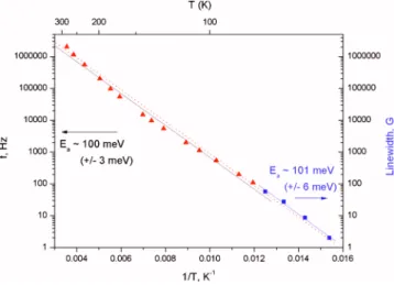
The temperature dependence of Ti3+-V共O兲 EPRs
line-width obeys an Arrhenius law关⌬B共T兲=⌬B0exp共-Ea/kT兲兴 as
shown in Fig. 3 共right scale兲. This agrees well with the
di-electric relaxation activation law which is also shown in Fig.
3 共left scale兲 confirming that the electronic localization on
Ti3+-V共O兲 centers is connected with the interfacial relaxation
leading to giant permittivity behavior. Within the IBLC model, we suggest that the Ti3+-V共O兲 centers create an en-ergy level close to the bottom of the BT conduction band which increase the grain conductivity through electronic hopping. Successive localization of such hopping electrons at the centers located close to grain boundaries lead to in-creased permittivity which relaxes with the same activation energy as the inner grain hopping conductivity, about 100 meV.
Additional electron trapping centers were also identified and they essentially confirm the barrier role of the silica shell
FIG. 1.共Color online兲 Photos and room temperature dielectric properties of SPS sintered and reoxidized BT@Si ceramics with different silica shell thickness: 0, 2, and 5 nm.
FIG. 2.共Color online兲 共a兲 EPR spectra recorded at 4 K in: a-BT500@Si5 “green composite,” b-BT500@Si5 SPS sintered and reoxidized, c-BT ceramics SPS sin-tered, d-BT ceramics SPS sintered and reoxidized, e-BT “green powder” with particles size 500 nm; 共b兲-EPR spectra of SPS sintered and reoxidized BT500@Si5 composite recorded at several temperatures: a—4 K, b—20 K, c—50 K, d—60 K, and e—100 K共intensity multiplied by 2兲.
as already observed for Ti3+related centers. For instance, the
signal of Fe3+fully disappears in the case of the SPS sintered
BT as expected from its reduction to low spin Fe2+ 共S=0兲,
while it is still present in the SPS sintered coated samples 关see spectra c and b in Fig. 2共a兲兴. This confirms the silica shell influence on the limited reoxidation of core-shell com-posites and hence on the valence state of intrinsic and impu-rity ions.
Another possible mechanism of electron localization in BT is the formation of polaronic type defects which also were observed in both BT and BT@Si ceramics,共see Fig.2兲.
Small polarons are very sensitive to the local stress indicat-ing their location in vicinity of grain boundaries or compos-ite interface. Broad intensive line observed only in BT@Si ceramics 关spectrum b in Fig. 2共a兲兴 in the magnetic field re-gion 3500–3750 G can be attributed to defects located at composite interface. The discussion on the detailed model for such defects is out of the scope of the present paper and will require further investigations.
We propose that the unprecedented room temperature permittivity and strong maximum in the dielectric losses with thermal activation energy between 0.1–0.4 eV observed in some oxides, can be ascribed to the electron trapped at oxygen vacancy with further localization at one of host lat-tice cation, and accumulation at 2D defects such as grain boundaries in ceramics. In particular, in BT based ceramics, the hopping conductivity among Ti3+-V共O兲 defects induces
such space charges at internal barriers. The dynamics of these space charges is thus intimately related to the hopping mobility of electrons at Ti3+-V共O兲 as shown from the similar
activation energy for the dielectric relaxation and for the EPR linewidths. As a consequence, the giant dielectric be-havior of BaTiO3 based ceramics can be ascribed to
elec-tronic excitations. This is an important result for the antici-pated use of these materials in supercapacitors. Indeed, all commercially available supercapacitors are based on ionic charges which accumulate at interfaces. Such ionic accumu-lation raises several issues such as slow dynamics and long
term stability resulting from large lattice distortions. In this respect, electron-based supercapacitors may provide interest-ing opportunities.
To summarize, thanks to the combination of core-shell architecture and SPS we have demonstrated an efficient way to control and stabilize oxygen–deficiency-related defects in BT-based ceramics共BaTiO3@ SiO2兲. EPR has allowed iden-tifying charged defects responsible for both color change and extrinsic giant dielectric properties of reduced BT core. In addition, a close link between the macroscopic dielectric re-laxation and the microscopic dynamics of charged defects was clearly evidenced: the value of activation energy of Ti3+-V共O兲 centers calculated from EPR lies in the same
range of that obtained from the dielectric measurements 共Ea⬵0.1 eV兲. Since this activation energy is similar in
sev-eral different oxides1–5 we suggest that shallow trap levels close to the bottom of the conduction band do occur in all these materials. Evidencing such defects through appropriate EPR investigations in these many materials would give a strong microscopic support to the internal barrier layer ca-pacitor model.6
We acknowledge financial support from the European Community through the FAME Erasmus Mundus program, from the French National Agency for Research under Con-tract No. ANR NANO4F and from Ukrainian-French ex-change program DNIPRO 19716PB. We also thank A. Ville-suzanne and M. Pollet for valuable advice for the critical reading of article.
1A. P. Ramirez, M. A. Subramanian, M. Gardel, G. Blumberg, D. Li, T.
Vogt, and S. M. Shapiro,Solid State Commun. 115, 217共2000兲.
2D. Capsoni, M. Bini, V. Massarotti, G. Chiodelli, M. C. Mozzatic, and C.
B. Azzoni,J. Solid State Chem. 177, 4494共2004兲.
3J. Wu, C.-W. Nan, Y. Lin, and Y. Denget,Phys. Rev. Lett. 89, 217601
共2002兲.
4N. Ikeda, H. Ohsumi, K. Ohwada, K. Ishii, T. Inami, K. Kakurai, Y.
Murakami, K. Yoshii, S. Mori, Y. Horibe, and H. Kitô,Nature共London兲
436, 1136共2005兲.
5I. P. Raevski, S. A. Prosandeev, A. S. Bogatin, M. A. Malitskaya, and L.
Jastrabik,J. Appl. Phys. 93, 4130共2003兲.
6C. D. Sinclair, T. B. Adams, F. D. Morrison, and A. R. West,Appl. Phys. Lett. 80, 2153共2002兲.
7B. E. Conway, Electrochemical Supercapacitors: Scientific Fundamentals
and Technological Applications共Springer, New York, 1999兲.
8M. Maglione, in Springer Series of Topics in Solid-State Sciences, edited
by V. S. Vikhnin and G. K. Liu共Springer, New York, 2011兲.
9O. Trithaveesak, J. Schubert, and Ch. Buchal,J. Appl. Phys. 98, 114101
共2005兲.
10L. Qiao and X. F. Bi,J. Phys. D: Appl. Phys. 42, 175508共2009兲. 11S. Mornet, C. Elissalde, O. Bidault, F. Weill, E. Sellier, O. Nguyen, and M.
Maglione,Chem. Mater. 19, 987共2007兲.
12U.-C. Chung, C. Elissalde, F. Mompiou, J. Majimel, S. Gomez, C.
Es-tournès, S. Marinel, A. Klein, F. Weill, D. Michau, S. Mornet, and M. Maglione,J. Am. Ceram. Soc. 93, 865共2010兲.
13U.-C. Chung, C. Elissalde, C. Estournès, and M. Maglione,Appl. Phys. Lett. 94, 072903共2009兲.
14V. V. Laguta, A. M. Slipenyuk, I. P. Bykov, M. D. Glinchuk, M. Maglione,
D. Michau, J. Rosa, and L. Jastrabik,Appl. Phys. Lett.87, 022903共2005兲.
15S. Lenjer, O. F. Schirmer, and H. Hesse,Phys. Rev. B 66, 165106共2002兲. 16V. V. Laguta, A. M. Slipenyuk, I. P. Bykov, M. D. Glinchuk, M. Maglione,
A. G. Belous O. I. V’yunov, J. Rosa, and L. Jastrabik,J. Appl. Phys. 97,
073707共2005兲. FIG. 3.共Color online兲 Dielectric relaxation time 共left scale, taken from Ref.
13兲 and Ti3+-V共O兲 linewidth vs temperature in an Arrhenius scale. The
com-mon slope共100 meV兲 of both lines calls for a common origin for these two mechanisms.