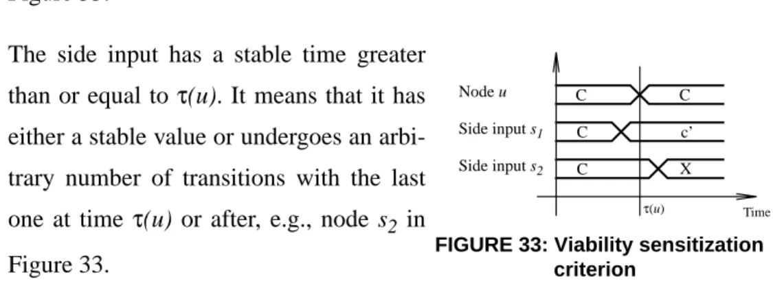
Détermination des bornes de
l’activité de commutation des
circuits logiques
par Jindrich Zejda
Département d’Informatique et de Recherche Opérationnelle Faculté des Arts et des Sciences
Thèse présentée à la Faculté des études supérieures en vue de l’obtention du grade
de Philosophiæ Doctor (Ph. D.) en Informatique
Mars, 1999
Bounding of Switching Activity in
Logic Circuits
by Jindrich Zejda
Department of Computer Science and Operational Research Faculty of Arts and Sciences
Thesis presented to the Faculty of Graduate Studies in partial fulfillment of the requirements to obtain the grade
of Philosophiæ Doctor (Ph. D.) in Computer Science
March, 1999
Cette thèse intitulée:
Détermination des bornes de
l’activité de commutation des
circuits logiques
présente par Jindrich Zejda
a été évaluée par un jury composé des personnes suivantes:
El Mostapha Aboulhamid . . . président-rapporteur Eduard Cerny . . . directeur de recherche Nicolas C. Rumin . . . co-directeur de recherche Marc Feeley . . . membre du jury
John P. Hayes . . . examinateur externe
Abstract
Electronic systems became an essential component of our lives. The demand for increased functionality is satisfied by higher integration which, however, make the design process more complex and introduces new problems. These problems must be considered in every step involved in the design of electronic systems.
One of these steps is verification - checking, whether what is manufactured will work properly. Among several properties that must be verified, power consump-tion is becoming more important than ever before. In the most commonly used CMOS technology a considerable amount of power is consumed due to switching which is described by switching activity. Switching activity in its broad sense is a measure of topological and temporal distribution of signal transitions for given operating environment of the circuit. This thesis addresses the problem of estima-tion of switching activity.
The thesis presents algorithms, implementation, and results of a new method based on constraint resolution for finding an upper bound on switching activity in the combinational part of a synchronous sequential circuit. The obtained switching activity is the major component for computing circuit power consumption (peak power) and several reliability parameters (e.g., voltage drops in power busses, electromigration). It is a static (input-pattern independent) method. The constraint system representing the circuit is built of constraints defined by gates and the oper-ating environment of the circuit. The variables of the constraint system are all pos-sible waveforms abstracted into four classes and expressed as sets of transitions for each unit of discrete time. The constraints of the constraint system are derived from the gates. Each gate is translated into a projection function which constrains each of its terminals based on the values on all other terminals independently of the netlist distinction between gate inputs and outputs. The method rapidly
com-putes an upper bound on the switching activity. The bound is further tightened by case analysis.
The constraint system captures only local relations between nets and gates. Two major techniques were used to capture a global picture of the circuit and use this acquired information to speed up or improve the analysis. They are reconvergent region analysis and global learning.
The method has two major applications: estimation of peak power and estimation of peak current. Both application were tested with our C++ implementation on ISCAS’85 benchmark circuits and the quality of the results for different heuristics was compared. The results show that each heuristic is more suitable for a different type of circuit. The method achieved values of about 1.5 to 3x, and 1.3 to 4x for the ratio of the upper and lower bounds of the switching and peak switching activ-ity, respectively. The method was also compared with exhaustive simulation on a set of MCNC circuits. The exact1 value of peak switching activity (peak current) was obtained for all tested MCNC circuits. The exact value of switching activity (power) was obtained on most of the tested MCNC circuits.
The current implementation supports the fixed gate delay model and shares most of the code with a timing verification method based on constraint resolution. The performance is further improved by a parallel implementation of the case analysis on a network of inexpensive workstations. The parallel configuration consists of one master and many slaves. The master is responsible for maintaining the current state of the search space, dynamically deciding which parts must be searched, and distributing jobs to slaves. The scheduling algorithm is slave-failure safe and the master performs periodic state saving for recovery from its own eventual failure. Our C++ implementation shows speedup of 8 on a homogeneous network of 10 workstations, and 47 on a heterogeneous network of 87 workstations.
1. “Exact value” means that the lower bound from the simulation is equal to the upper bound (under the fixed delay gate model).
Résumé
Les systèmes électroniques sont devenus une partie essentielle de notre vie. On peut les trouver partout, que ce soit dans les systèmes de contrôle de feux d’inter-section, les systèmes de navigation pour avions et satellites, les systèmes de télé-communication ou les ordinateurs de haute performance. La réponse à la demande de nouvelle fonctionnalité et de plus grande performance nécessite une plus grande intégration. Cette grande intégration génère de nouveaux problèmes - qui ont pu être négligés jusqu’alors. Mais aujourd’hui on doit considérer tout ces problèmes dans chaque étape du processus de développement des systèmes électroniques.
Une de ces étapes est la vérification - étape qui assure qu’une fois le produit est fabriqué, il fonctionne correctement. Parmi les propriétés que l’on doit vérifier, la consommation du courant devient plus importante que jamais. Pour la technologie la plus utilisée aujourd’hui - CMOS - la plus importante partie du courant est cau-sée par la commutation des signaux logiques qui est décrite par l’activité de com-mutation. L’activité de commutation est une mesure de distribution de transition temporelle et spatiale dans le circuit sous une condition d’environnement donnée. Cette thèse s’adresse au problème d’estimation de l’activité de commutation.
La thèse présente les algorithmes, l’implémentation, et les résultats d’une nouvelle méthode pour trouver une borne supérieure d’activité de commutation dans la par-tie combinatoire d’un circuit synchrone séquenpar-tiel basée sur une résolution de con-traintes. L’activité de commutation est un composant majeur pour le calcul de consommation du courant d’alimentation du circuit, et pour plusieurs paramètres de fiabilité (par exemple chute de voltage dans des réseaux de distribution du cou-rant, ou electromigration). La méthode est statique, c’est à dire que son résultat est indépendant des vecteurs de test sur les entrées du circuit.
L’idée de base de la méthode est la suivante: Le circuit électronique est considéré comme un système de con-trainte. Les portes logiques et l’environnent du circuit sont représentés par des
con-traintes. Les signaux du circuit sont représentés par les variables du système de contraintes. Toutes les ondes de signaux sur un nœud du circuit sont groupées en quatre classes et représentés par une ensemble de transitions pour chaque intervalle de temps (Figure 1). Les classes sont indépendantes - si une onde réelle est représentée par un sous-ensemble de classe, elle ne peut avoir aucune transition dans n’importe quelle autre classe. Cette propriété est utilisée dans l’analyse des cas décrit plus tard.
Chaque porte logique intro-duit des relations entre les ondes abstraites qui contraig-nent tous ses terminaux. La valeur de chaque nœud est exprimée comme l’intersec-tion de la valeur du nœud courant et les fonctions de portes, dans les deux direc-tion - sorties à entrée, et
entrée à sorties (Figure 2). Cette méthode permet de calculer rapidement une borne supérieure de l’activité de commutation.
FIGURE 1: Onde abstraite
8 -1 0 1 2 3 4 c00 c01 c10 c11 Classes de Ensemble de transitions L’ensemble de transitions dans la classe 00 dans l’intervalle numéro 2
Temps discret
Temps i correspond à l’inter-valle[ri,ri+1) du temps réel
Nœud du circuit ondes
FIGURE 2: Le système de contraints
x1 x2 g1 g2 g3 S1 S2 S3 ∩ g1-1 ∩ S1 g1-1 S2 S3
S variable ∩opération dépendance
g2-1 g2 g3 g1 ∩ S1=AWI∩g-11(S2,S3) S2=AWI∩g-11(S1,S3) S3= g1(S1,S2)∩ -1 -1 AWI AWI g-13 g2(...)∩ g3(...) Circuit Le système de contraints
Dans la thèse, la méthode est illustrée par un petit circuit -c17. Si le circuit est une partie combinatoire d’un circuit séquentiel, les entrées peuvent changer seulement par temps d’horloge (zero, observées les ondes sur nœuds 0 jusqu’à 4 dans Figure 3). Les autres ondes sont le résultat de propa-gation de ces contraintes (Figure 3). Dans cet exemple toutes les portes ont un délai unité.
Les ondes abstraites contiennent tout les ondes réelles possibles. Donc, l’activité de commutation (nombre de transitions pendant une période d’horloge) est cal-culée comme la somme de nombre de transitions, pour chaque onde abstraite. Dans le Figure 3 c’est 15. En utilisant la librairie physique cette valeur peut être convertie à la consommation de courant.
Pour évaluer la fiabilité du cir-cuit, il est important de cal-culer le courant maximal dans le réseau. Le courant maximal peut être calculé à partir du profil d’activité de commuta-tion qui est obtenu en comp-tant les transitions de toutes les
ondes pendant chaque intervalle de temps individuellement (Figure 4).
FIGURE 3: Circuit c17 - propagation nationale 0 1 2 3 4 5 6 7 8 9 10 0 -1 0 1 2 3 4 c00 c01 c10 c11 1 -1 0 1 2 3 4 c00 c01 c10 c11 2 -1 0 1 2 3 4 c00 c01 c10 c11 3 -1 0 1 2 3 4 c00 c01 c10 c11 7 -1 0 1 2 3 4 c00 c01 c10 c11 8 -1 0 1 2 3 4 c00 c01 c10 c11 9 -1 0 1 2 3 4 c00 c01 c10 c11 10 -1 0 1 2 3 4 c00 c01 c10 c11 4 -1 0 1 2 3 4 c00 c01 c10 c11 5 -1 0 1 2 3 4 c00 c01 c10 c11 6 -1 0 1 2 3 4 c00 c01 c10 c11
FIGURE 4: Circuit c17 - profile d’activité de commutation 0 20 40 0 1 2 3 4 30 50 10 Nombre de Transitions Temps
Ensuit, la borne supérieure est améliorée par une analyse de cas basée sur l’indépendance des classes d’ondes dans les ondes abstraites. Dans cet exemple, l’analyse de cas a déterminé que la borne supérieure est 14 transitions pour une période d’horloge. Le nombre de transitions maximale pour un intervalle du temps n’était pas amélioré: la valeur initiale est la valeur exact.
Le système de contraintes exprime seulement la relation locale entre des portes et nœuds du circuit. Deux autres techniques ont été introduites pour uti-liser plus d’information sur le circuit: l’analyse de régions de reconvergence
et l’apprentissage global (Figure 5). La méthode implémentée en C++ a été testée sur l’ensemble de circuits benchmark ISCAS’85 et l’efficacité de plusieurs heuris-tiques a été comparée. Les résultats ont démontrés que l’efficacité de chaque heu-ristique dépend de la topologie et de la fonctionnalité du circuit. La borne supérieure était de 1.5 à 3x la borne inférieure de l’activité de commutation (con-sommation) et 1.3 à 4x de l’activité de commutation maximale (courant maximal). D’autres propriétés de la méthode ont été testées sur les circuits MCNC et circuits ISCAS’85 avec délais de portes d’une librairie industrielle lsi_10k. Nous avons obtenu la valeur exacte1 sur la majorité des circuits.
L’implémentation qui a été testée supporte des modèles de portes avec délais fixes et elle partage une grande partie du code avec une méthode de vérification tempo-relle basée sur la résolution de contraintes. La performance est ensuite améliorée par l’analyse de cas sur un réseau de stations de travail. La configuration parallèle est centralisée (étoile). La station au centre maintient l’espace de recherche, anal-yse, décide quelle parties sont intéressantes, et distribue les tâches aux autres (esclave). L’algorithme de répartition est résistant aux fautes sur les esclaves et la
1. “La valeur exacte” c’est à dire que la borne inférieurs obtenu par simulation est égale à la borne supérieure (sous les modèles de portes avec délais fixes).
FIGURE 5: L’apprentissage sur valeurs Booléennes A B En avant: B=1⇒ A=1 A=0⇒ B=0 En arrière:
station au centre préserve périodiquement son état sur un disque. Notre implémen-tation parallèle a démontré l’accélération d’un facteur 8 sur 10 simplémen-tations de travail et 47 sur un réseau hétérogène de 87 stations.
Table of Contents
Abstract ... iv
Résumé ... vi
Table of Contents ... xi
List of Tables ... xviii
List of Figures ... xxi
List of Symbols, Keywords, and Abbreviations ... xxix
Preface ... xxxv
Chapter 1:
Introduction ... 1
1-1. Design flow ... 2
1-1.1 General design flow ... 2
1-1.2 Design flow in electronic industry ... 3
1-2. Verification of electronic circuits ... 6
1-2.1 Classification of verification methods ... 6
1-2.1.1 Functional verification ... 6
1-2.1.2 Testability ... 7
1-2.1.3 Timing verification ... 8
1-2.1.4 Verification of power consumption ... 8
1-2.1.5 Verification properties on a behavioral model ... 9
1-2.1.6 Verification of an RTL description ... 10
1-2.1.7 Verification at the gate level ... 11
1-2.1.8 Verification at the transistor level ... 12
1-2.1.9 Verification at the layout (mask) level ... 14
1-2.1.10 Verification by simulation ... 15
1-2.1.11 Formal verification ... 15
1-2.2 Timing verification ... 17
1-2.3 Verification of power consumption ... 20
1-3. The problem of timing and power verification and the contributions of this thesis ... 21
1-3.1 Problem definition ... 22
1-3.2 Outline of the proposed solution to bounding switching activity ... 23
1-3.3 Original contributions ... 24
Chapter 2:
Verification methods for timing and
switch-ing activity ... 27
2-1. Modeling ... 28
2-1.1 Timing and power properties of synchronous circuits ... 28
2-1.2 Delay representation ... 31
2-1.3 Gate delay models ... 32
2-1.4 Combinational circuit delay model ... 32
2-1.5 The false path problem ... 34
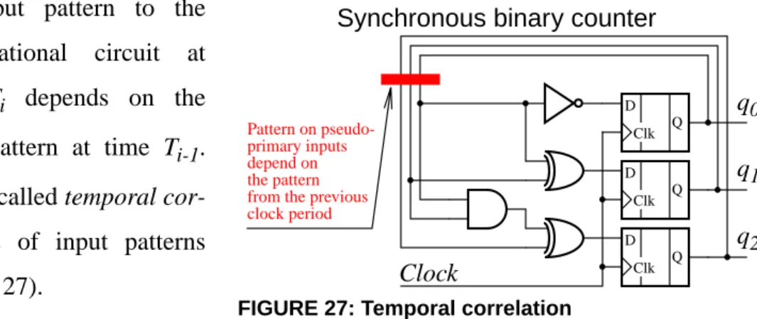
2-1.6 Spatial and temporal correlation ... 35
2-1.7 Component parameter correlation ... 36
2-1.8 Toggle power ... 38
2-1.9 Conversion from switching activity to power ... 38
2-2. Universal and timing-specific verification methods ... 40
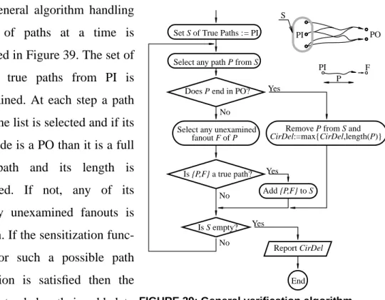
2-2.1 Exhaustive simulation ... 40 2-2.2 Path-oriented methods ... 41 2-2.2.1 Static sensitization ... 42 2-2.2.2 Dynamic sensitization ... 43 2-2.2.3 Viability sensitization ... 44 2-2.2.4 Floating-mode sensitization ... 44
2-2.2.5 Lower bound sensitization ... 46
2-2.2.6 Vigorous sensitization ... 47
2-2.2.7 Comparison of several sensitization criteria ... 47
2-2.3 Algorithms for solving the false path problem ... 48
2-2.3.1 An algorithm for computing the longest viable path ... 48
2-2.3.2 An algorithm based on ATPG ... 50
2-2.4 Optimization-based methods ... 53
2-2.4.1 An algorithm for computing the exact circuit delay ... 53
2-2.4.2 An algorithm based on constraint satisfaction ... 54
2-2.4.3 Methods treating correlated component delays ... 54
2-2.5 Various problems and notes ... 57
2-2.5.1 Transition delay and the minimum clock period ... 57
2-2.5.2 Zero-width glitches ... 58
2-2.5.3 Standardization in delay and power calculation ... 58
2-3. Power verification methods ... 60
2-3.1 Random simulation ... 60
2-3.2 Probabilistic power estimation methods ... 61
2-3.2.1 Interval gate delays and power analysis ... 65
2-3.3 High-level approaches to power verification ... 68
2-3.3.1 High-level power analysis ... 68
2-3.3.2 Optimization of circuits for low power at the circuit level . 70 2-3.3.3 Optimization of circuits for low power at the logic level ... 71
2-3.3.4 High level power optimization ... 73
2-3.3.5 System and software level power optimization ... 74
2-3.4 Low-level approaches to power verification ... 75
2-3.5 Pattern independent methods for computing an upper bound on pow-er dissipation ... 77
2-3.5.1 Uncertainty waveforms and partial input enumeration ... 77
2-3.5.2 Power estimation based on constraint resolution ... 78
2-3.6 Power estimation in sequential circuits ... 79
2-3.7 Methods analyzing current distributions on a chip ... 79
2-3.7.1 Voltage drops ... 79
2-3.7.2 Current distributions ... 80
2-4. Literature survey - conclusions ... 81
Chapter 3:
Bounding switching activity using
con-straint resolution ... 83
3-1. Circuit modeling - the constraint system ... 83
3-1.1 Waveform classification ... 84
3-1.2 Operations over space of abstract waveforms ... 87
3-1.3 Power analysis ... 91
3-1.3.1 Initial propagation and estimate ... 92
3-1.3.2 Transition counting ... 92
3-2. Case analysis ... 93
3-2.1 Principles of case analysis ... 93
3-2.2 Case analysis on waveform classes ... 94
3-2.3 Case analysis in a circuit ... 95
3-2.4 Decision tree ... 96
3-2.5 Case analysis algorithms ... 97
3-2.6 Net selection for case analysis ... 98
3-2.7 Properties of the constraint system and of the case analysis ... 99
3-3. Example ... 100
3-4. Reconvergence analysis ... 104
3-4.1 Introduction ... 104
3-4.1.1 Use of reconvergent regions in fault analysis ... 105
3-4.1.2 Complexity of fault analysis and region overlap ... 105
3-4.1.3 Secondary reconvergence ... 106
3-4.2 Fault analysis based on reconvergent regions ... 107
3-4.2.1 The fault model and dynamic reductions ... 108
3-4.2.2 Results ... 110
3-4.3 Reconvergence in timing and power verification ... 110
3-4.4 Algorithm for reconvergence analysis ... 112
3-5. Learning ... 114
3-5.1 Global implications in ATPG ... 115
3-5.2 Use of global implications in the analysis of switching activity .. 116
3-6.1 Fanout ... 118
3-6.2 Fanout on primary inputs ... 119
3-6.3 Dynamically created list of nets ... 120
3-6.4 Reconvergent regions ... 121
3-6.5 Other heuristics for net selection in case analysis ... 121
3-7. Use of timing constraints ... 122
3-8. Implementation ... 122
Chapter 4:
Experimental Results ... 123
4-1. Lower bound simulation ... 124
4-2. The initial upper bound on switching activity ... 126
4-3. Case analysis on nets sorted by decreasing fanout ... 127
4-3.1 FANOUT without learning for 1000 decisions ... 127
4-3.2 FANOUT without learning for 10000 decisions ... 131
4-3.3 FANOUT with learning for 1000 decisions ... 133
4-3.4 FANOUT with learning for 10000 decisions ... 134
4-4. Case analysis on primary inputs sorted by decreasing fanout ... 135
4-4.1 PIFAN without learning for 1000 decisions ... 135
4-4.2 PIFAN with learning for 1000 decisions ... 135
4-5. Case analysis on closing nets and primary inputs sorted by decreas-ing fanout ... 136
4-5.1 RCVFAN without learning for 1000 decisions ... 136
4-5.2 RCVFAN with learning for 1000 decisions ... 136
4-6. Comparison of heuristics for net selection ... 137
4-7. Comparison of PCA and HPCA ... 139
4-8. Reaching the exact value ... 141
4-9. Use of timing constraints ... 142
4-10. Comparison with other methods ... 144
Chapter 5:
Parallel Case Analysis ... 145
5-1. Algorithm for parallel case analysis ... 145
5-1.1 Static search-space-division algorithm ... 146
5-1.2 Dynamic search-space-division algorithm ... 147
5-2. Example of Parallel Case Analysis ... 151
5-3. Implementation ... 153
5-3.1 The decision tree data structure ... 155
5-3.2 Implementation layers ... 157
5-3.3 Master ... 158
5-3.5 Slave ... 159
5-3.6 Network layer ... 159
5-3.7 Object to message translation ... 159
5-3.8 MIF export interface ... 160
5-3.9 File descriptors ... 160
5-4. Experimental results ... 161
5-5. Performance measures for parallel processing ... 162
5-5.1 Analysis on a small number of computers ... 164
5-5.2 Analysis on a small number of computers for a constant time ... 168
5-5.3 Analysis on a large number of computers ... 169
5-5.4 Depth of local exploration ... 171
5-6. Theoretical model ... 173
5-6.1 Properties necessary for the application of our parallel algorithm ... 173 5-6.2 Speedup ... 174
5-6.3 Conditions for the best performance ... 176
5-6.4 Theoretical analysis of our practical results on 87 machines ... 176
5-7. Parallel implementation - conclusions ... 178
Chapter 6:
Voltage Drops in Power Busses ... 179
6-1. Switching Activity Profile Algorithm ... 179
6-2. Example of Switching Activity Profile Calculation ... 181
6-3. Implementation of Switching Activity Profile Analysis ... 183
6-4. Experimental results ... 184
6-4.1 Peak switching activity in ISCAS’85 circuits ... 185
6-4.2 Peak switching activity in the MCNC circuits ... 189
Chapter 7:
Conclusions ... 194
7-1. Constraint system ... 195
7-2. Case analysis ... 195
7-2.1 Initial upper bound on switching activity ... 195
7-2.2 Case analysis algorithms ... 196
7-2.3 Heuristics for net selection ... 196
7-2.4 Parallel case analysis ... 196
7-3. Comparison with other methods ... 197
7-4. Contributions of this thesis ... 199
7-5. Future research ... 199
7-5.1 Circuit models ... 200
7-5.3 Conversion of switching activity into electric current ... 200
7-5.4 Uses of parallel case analysis ... 200
Index ... 201
References ... 211
Appendices ... ccxxviii
Appendix A: Technical Documentation and Utilization ccxxviii
A-1. Architecture ... ccxxviiiA-1.1 Modules ... ccxxviii A-1.2 Revision Control ... ccxxix A-1.3 Benchmarks ... ccxxx A-1.4 Source Code ... ccxxx
A-2. Modules ... ccxxxi
A-2.1 Parser interface and the top level (ic) ... ccxxxii A-2.1.1 Shared part ... ccxxxii A-2.1.2 Switching activity analysis (PW) ... ccxxxiii A-2.2 Circuit representation (udm) ... ccxxxix A-2.2.1 Constraint system fixpoint ... ccxl A-2.2.2 The data structure representing a circuit net ... ccxl A-2.2.3 The data structure representing a gate ... ccxlii A-2.2.4 The data structure representing a circuit ... ccxliii A-2.3 Timing (ta) ... ccxlv A-2.4 Switching activity (pw) ... ccxlvi A-2.5 Topological analysis (stat) ... ccxlvii A-2.6 Case analysis (anal) ... ccxlvii A-2.7 Partitioning (part) ... ccxlviii A-2.8 Learning (learn) ... ccxlviii A-2.9 Reconvergence (reconv) ... ccxlix A-2.10 Parallel (network) ... ccl A-2.11 Auxiliary (else) ... ccl
A-3. Utilization ... ccli
A-3.1 Viewing the circuit netlist ... ccli A-3.2 Timing analysis ... cclii A-3.3 Switching activity analysis ... cclii A-3.4 Decision function ... cclii A-3.5 Case analysis ... ccliii A-3.6 Parallel case analysis ... ccliii A-3.7 Manual mode ... ccliv A-3.8 Various options ... ccliv
Appendix B: Conflict of N messages ... cclvi
Appendix C: Decision Trees ... cclvii
Acknowledgments ... cclxvi
Curriculum vitae ... cclxvii
List of Tables
TABLE I: Classification of verification methods ... 6
TABLE II: ISCAS’85 circuits [BrgF85] ... 124
TABLE III: Lower bounds ... 125
TABLE IV: Initial upper bound on switching activity ... 126
TABLE V: Comparison of lower bounds and the initial upper bounds ... 127
TABLE VI: Case analysis on all nets sorted by fanout, 1000 decisions ... 128
TABLE VII: Case analysis on all nets sorted by fanout, 10000 decisions ... 131
TABLE VIII: Case analysis on all nets, fanout, learning, 1000 decisions ... 133
TABLE IX: Case analysis on all nets, fanout, learning, 10000 decisions ... 134
TABLE X: Case analysis on PIs sorted by fanout, 1000 decisions ... 135
TABLE XI: Case analysis on PIs, fanout, with learning, 1000 decisions ... 135
TABLE XII: Case analysis on closing nets, 1000 decisions ... 136
TABLE XIII: Case analysis on closing nets of reconvergent regions, with learn-ing, 1000 decisions ... 137
TABLE XIV: Comparison of heuristics for net selection ... 138
TABLE XV: Comparison of PCA and HPCA, 11 ISCAS’85 circuits in total 139 TABLE XVI: PCA, 1000 decisions ... 140
TABLE XVII: HPCA, 1000 decisions ... 140
TABLE XVIII: PCA, 10000 decisions ... 140
TABLE XIX: HPCA, 10000 decisions ... 140
TABLE XX: SAV in MCNC circuits, PIFAN, no_progress=1000 ... 141
TABLE XXI: Comparison of lower bounds and the final upper bounds ... 142
TABLE XXII: Topological delay and lower bound circuit delay ... 143
TABLE XXIV: Network media throughput ... 149
TABLE XXV: Calibration table c1908, 1002 decisions ... 164
TABLE XXVI: Comparison of SPECint92 with obtained performance ... 165
TABLE XXVII: Analysis results - circuit c1908, 1002 decisions, 1 to 10 comput-ers in parallel ... 166
TABLE XXVIII: Analysis results - circuit c1908, 30 minutes, 1 to 10 computers in parallel ... 168
TABLE XXIX: Analysis results - circuit c1908, 3*106decisions, 87 computers in parallel ... 170
TABLE XXX: Topological data for ISCAS85_lsi10k benchmarks ... 185
TABLE XXXI: Initial, and simulation switching activity for ISCAS85_lsi10k benchmarks ... 185
TABLE XXXII: PSAV (Peak Current) in ISCAS85_lsi10k circuits with no_progress=10, heuristic FANOUT ... 186
TABLE XXXIII: PSAV (Peak Current) in ISCAS85_lsi10k circuits with no_progress=100, heuristic FANOUT ... 186
TABLE XXXIV: PSAV (Peak Current) in ISCAS85_lsi10k circuits with no_progress=1000, heuristic FANOUT ... 187
TABLE XXXV: PSAV (Peak Current) in ISCAS85_lsi10k circuits with no_progress=1000, heuristic PIFAN ... 187
TABLE XXXVI: Comparison of our results with [KrNH95]; PSAV using FANOUT, no_progress=1000 ... 188
TABLE XXXVII: Topological data for MCNC benchmarks ... 189
TABLE XXXVIII: Initial and simulation switching activity for MCNC benchmarks ... 189
TABLE XXXIX: PSAV (Peak Current) in MCNC circuits with no_progress=10 ...190
TABLE XL: PSAV (Peak Current) in MCNC circuits with no_progress=100 ... 190
TABLE XLI: PSAV (Peak Current) in mcnc circuits with no_progress=1000 ... 191
TABLE XLII: PSAV (Peak Current) in mcnc circuits with no_progress=106.. 191 TABLE XLIII: PSAV (Peak Current) in MCNC circuits with no_progress=106,
List of Figures
FIGURE 1: Onde abstraite ... vii
FIGURE 2: Le système de contraints ... vii
FIGURE 3: Circuit c17 - propagation nationale ... viii
FIGURE 4: Circuit c17 - profile d’activité de commutation ... viii
FIGURE 5: L’apprentissage sur valeurs Booléennes ... ix
FIGURE 6: General Design flow ... 2
FIGURE 7: Design flow ... 4
FIGURE 8: Task of formal verification ... 7
FIGURE 9: Behavioral description ... 9
FIGURE 10: RTL description ... 10
FIGURE 11: Gate-level description ... 11
FIGURE 12: Transistor level description ... 12
FIGURE 13: Layout description ... 14
FIGURE 14: Verification by Simulation ... 15
FIGURE 15: Formal verification ... 15
FIGURE 16: Synchronous sequential circuit ... 28
FIGURE 17: Timing properties of the synchronous circuit ... 28
FIGURE 19: Setup and hold time considering clock distribution delay ... 29
FIGURE 18: Clock distribution delay ... 29
FIGURE 20: CMOS gate power consumption ... 30
FIGURE 21: Switching behavior of a synchronous circuit ... 31
FIGURE 22: Gate delay models ... 32
FIGURE 25: False path demonstration ... 34 FIGURE 24: Path and side inputs to the path ... 34 FIGURE 26: Spatial correlation ... 35 FIGURE 27: Temporal correlation ... 36 FIGURE 28: Independent and correlated gate delays ... 37 FIGURE 29: Glitching ... 38 FIGURE 30: CMOS inverter ... 38 FIGURE 31: Static sensitization criterion ... 42 FIGURE 32: Dynamic sensitization criterion ... 43 FIGURE 33: Viability sensitization criterion ... 44 FIGURE 34: Floating-mode sensitization criterion ... 45 FIGURE 35: The difference between the viability and floating-mode
sensitiza-tion criteria ... 46 FIGURE 36: Lower bound sensitization criterion ... 46 FIGURE 37: Vigorous sensitization criterion ... 47 FIGURE 38: Categorization of sensitization criteria ... 48 FIGURE 39: General verification algorithm handling a set of paths at a time . 49 FIGURE 40: Making a circuit fanout tree ... 50 FIGURE 41: Two-level circuit representing ENF ... 50 FIGURE 42: Moving inverters to the primary inputs ... 52 FIGURE 43: Fault injection ... 52 FIGURE 44: Transition delay validity as a minimal clock period ... 58 FIGURE 45: Signal probabilities - AND and XOR gate ... 61 FIGURE 46: Glitching sensitivity of 2-input AND and XOR gates ... 62 FIGURE 47: Probability waveform ... 63 FIGURE 48: Signal representation by histogram of number of transitions ... 66 FIGURE 49: Transition density waveforms and the gate model ... 66
FIGURE 50: Less pessimistic transition density ... 67 FIGURE 51: Activity waveforms ... 68 FIGURE 52: Capacitance feed-through effect ... 76 FIGURE 53: 2-input CMOS NAND gate ... 76 FIGURE 54: An uncertainty waveform ... 77 FIGURE 55: VLSI power supply network ... 79 FIGURE 56: Voltage drops in a power network tree structure ... 80 FIGURE 57: Abstract waveform ... 84 FIGURE 58: Set of transitions ... 84 FIGURE 59: Waveform classification and abstraction ... 86 FIGURE 60: Graphical representation of an abstract waveform ... 86 FIGURE 61: Local intersection ... 88 FIGURE 62: AND operation ... 89 FIGURE 63: Example of NOT operation ... 89 FIGURE 64: Gate network as a system of equations ... 91 FIGURE 65: Primary input abstract waveform ... 92 FIGURE 66: Identification of simple waveform with the largest number of
tran-sitions in an abstract waveform ... 93 FIGURE 67: Principle of case analysis ... 94 FIGURE 68: Case analysis on a single net ... 94 FIGURE 69: Case analysis on two nets ... 95 FIGURE 70: Initial state of the constraint system ... 95 FIGURE 71: Constraint system for A=01 ... 95 FIGURE 72: Constraint system for A=01, B=11 ... 96 FIGURE 73: Case analysis decision tree ... 96 FIGURE 74: Step of the frontier-type case analysis ... 97 FIGURE 75: Counting fanout ... 98
FIGURE 76: Circuit c17; all gates have unit delay. ... 100 FIGURE 77: Waveforms of c17 after initial forward propagation ... 101 FIGURE 78: Decision tree for c17, analysis on net 2 ... 101 FIGURE 79: Decision tree for c17, analysis on nets 2 and 6 ... 102 FIGURE 80: Waveforms of c17 for assignments 2:c01, 6:c10 ... 102 FIGURE 81: Decision tree for c17, complete analysis ... 103 FIGURE 82: Simple waveforms with transition count of 14 ... 103 FIGURE 83: Reconvergent stem and reconvergence gate ... 104 FIGURE 84: Closing gate ... 104 FIGURE 85: Reconvergent stem region ... 105 FIGURE 86: Primary (prg) and secondary (srg) reconvergence gates ... 106 FIGURE 87: Enlarged reconvergence regions ... 107 FIGURE 88: Disjoint subnetworks driven by exit lines ... 107 FIGURE 89: Consequence of exit line properties ... 108 FIGURE 90: Dropping faults, method “2” ... 109 FIGURE 91: Case analysis on overlapping reconvergent stem regions ... 111 FIGURE 93: Finding reconvergence gates - TAG1 ... 112 FIGURE 92: Finding reconvergence gates - TAG0 ... 112 FIGURE 94: Identifying reconvergent regions ... 113 FIGURE 95: Forest of reconvergent stem regions in c432 ... 114 FIGURE 96: Implication and learning ... 114 FIGURE 97: Learning - abstract waveforms ... 116 FIGURE 98: Learning - constraint B=c11 ... 116 FIGURE 99: Learning - effect of the learned implication ... 116 FIGURE 100: Learning - propagation due to a reduced side input ... 117 FIGURE 101: Learning along reconvergent regions ... 117 FIGURE 102: Fanout influence ... 118
FIGURE 103: Fanout influence - constraint A=c00 ... 118 FIGURE 104: Fanout influence - constraint B=c00 ... 119 FIGURE 105: Fanout influence - constraint B=c00 when S1=c11 ... 119 FIGURE 106: Dynamically created list of nets ... 120 FIGURE 107: Simulation of ISCAS’85 circuits ... 124 FIGURE 108: Lower bounds on delay and switching activity in c432 ... 125 FIGURE 109: Lower bounds on delay and switching activity in c499 ... 125 FIGURE 110: Lower bounds on delay and switching activity in c1908 ... 126 FIGURE 111: Lower bounds on delay and switching activity in c6288 ... 126 FIGURE 112: Lower bounds on delay and switching activity in c7552 ... 126 FIGURE 113: Progress of case analysis, c17, fanout, up to 1000 decisions ... 128 FIGURE 114: Progress of case analysis, c432, fanout, up to 1000 decisions ... 128 FIGURE 115: Progress of case analysis, c499, fanout, up to 1000 decisions ... 128 FIGURE 116: Progress of case analysis, c880, fanout, up to 1000 decisions ... 129 FIGURE 117: Progress of case analysis, c1350, fanout, up to 1000 decisions . 129 FIGURE 118: Progress of case analysis, c1908, fanout, up to 1000 decisions . 129 FIGURE 119: Progress of case analysis, c2670, fanout, up to 1000 decisions . 129 FIGURE 120: Progress of case analysis, c3540, fanout, up to 1000 decisions . 129 FIGURE 121: Progress of case analysis, c5315, fanout, up to 1000 decisions . 130 FIGURE 122: Progress of case analysis, c6288, fanout, up to 1000 decisions . 130 FIGURE 123: Progress of case analysis, c7552, fanout, up to 1000 decisions . 130 FIGURE 124: Progress of case analysis, c499, fanout, up to 10000 decisions . 131 FIGURE 125: Progress of case analysis, c1908, fanout, up to 10000
deci-sions ... 132 FIGURE 126: Progress of case analysis, c2670, fanout, up to 10000
deci-sions ... 132 FIGURE 127: Progress of case analysis, c6288, fanout, up to 10000
FIGURE 128: Progress of case analysis, c1355, fanout, learning, 1000 decis. 133 FIGURE 129: Progress of case analysis, c2670, fanout, learning, 10k decis. .. 134 FIGURE 130: Comparison of heuristics in c1908 - 1002 decisions, CPU
time ... 138 FIGURE 131: Parallel case analysis with static division of the search space ... 146 FIGURE 132: Decision tree - c1908, 1000 decisions ... 147 FIGURE 133: Dynamic parallel case analysis ... 148 FIGURE 134: Fail-safe dynamic parallel case analysis ... 150 FIGURE 137: Parallel analysis - c17, second decision analysis ... 151 FIGURE 135: Network architecture - 2 slaves ... 151 FIGURE 136: Parallel analysis - c17, first 4 paths ... 151 FIGURE 138: Parallel analysis - c17, after the second decision analysis ... 152 FIGURE 139: Parallel analysis - c17, the third decision analysis ... 152 FIGURE 140: Parallel analysis - c17, the fourth decision analysis ... 152 FIGURE 141: Parallel analysis - c17, execution traces ... 153 FIGURE 142: CA tree as a heap ... 155 FIGURE 143: Path implementation ... 155 FIGURE 144: Heap architecture ... 156 FIGURE 145: C++ architecture of parallel case analysis ... 157 FIGURE 146: Upper bound as a functions of the number of decisions - c1908,
1002 decisions, 1, 6 and 10 CPUs ... 166 FIGURE 147: Upper bound in real time - circuit c1908, 1002 decisions, 1, 2, 4,
10 CPUs ... 167 FIGURE 148: Performance of parallel case analysis - decisions per second,
c1908, 1002 decisions, 1 to 10 CPUs ... 167 FIGURE 149: Upper bound as a function of the number of slaves - c1908, 30
minutes, 1 to 10 CPUs ... 169 FIGURE 150: Performance of parallel case analysis as a function of the number
FIGURE 151: Upper bound as a function of the number of decisions - c1908, 3*106 decisions, 87 CPUs ... 170 FIGURE 152: Depth of local decisions ... 171 FIGURE 153: Comparison of 1- and 2-level local decision analysis - number of
decisions, c1908, 10000 decisions, 6CPUs ... 171 FIGURE 155: Comparison of 1- and 2-level local decision analysis - real time,
c1908, 2 hours, 6 CPUs ... 172 FIGURE 154: Comparison of 1- and 2-level local decision analysis - real time,
c1908, 10000 decisions, 6 CPUs ... 172 FIGURE 156: Execution trace of parallel algorithm ... 174 FIGURE 157: Calculated speedup ... 177 FIGURE 159: Waveforms and the current profile of c17 after initial forward
propagation ... 181 FIGURE 158: Circuit c17; all gates have unit delay. ... 181 FIGURE 160: Decision tree for c17 ... 182 FIGURE 161: Test vector c17 (net4=c10) ... 182 FIGURE 162: Switching activity profile c17 ... 183 FIGURE 163: Architecture ... ccxxviii FIGURE 164: Directory tree ... ccxxx FIGURE 165: Directory tree - source files ... ccxxxi FIGURE 166: Circuit netlist and corresponding C++ classes ... ccxxxix FIGURE 168: Abstract waveform - UDMwaveformSet ... ccxli FIGURE 167: Net - UDMwaveforms ... ccxli FIGURE 169: Gate - UDMgate ... ccxlii FIGURE 170: UDMgatem ... ccxliii FIGURE 171: Circuit - UDM ... ccxliv FIGURE 172: Timing class - TAwaveform ... ccxlv FIGURE 173: Transition set class - PWwaveform ... ccxlvi FIGURE 174: Decision tree for c499 ... cclvii
FIGURE 175: Decision tree for c432 ... cclviii FIGURE 176: Decision tree for c880 ... cclix FIGURE 177: Decision tree for c1355 ... cclx FIGURE 178: Decision tree for c1908 ... cclxi FIGURE 179: Decision tree for c3540 ... cclxi FIGURE 180: Decision tree for c2670 ... cclxii FIGURE 181: Decision tree for c5315 ... cclxiii FIGURE 182: Decision tree for c17 ... cclxiii FIGURE 183: Decision tree for c6288 ... cclxiv FIGURE 184: Decision tree for c7552 ... cclxv
List of Symbols,
Keywords, and
Abbreviations
Arc The concept of timing arcs is a way to describe pin-to-pin delays of a gate. A typical timing library would have at least one arc per pin pair. Each arc can describe rise/fall interval (min/max) delay or have a power consumption information associated with it.
ASIC Application specific integrated circuit
BDD Binary decision diagram
BIST Built-in self test
bug Error causing faulty behavior, in hardware or software
CMOS Complementary metal-oxide semiconductor - a widely used technology to implement low-cost, medium-speed, mainly digital electronic cir-cuits
C++ C Plus Plus - a portable object oriented programming language
DRC Design rule check - generally a term for post-layout verification of geo-metrical objects which implement the circuit in form of PCBs or ASICs
DSM Deep Sub-Micron - related to design flow for fabrication with feature size under one micro meter, typically under 0.25 or 0.18 micro meter.
ECD Expected Current Distribution - time profile of current drawn by a cir-cuit with substantial statistical information for each interval of discrete time
EDA Electronic Design Automation
FANOUT Heuristic for selection of nets and their order for case analysis based on
fanout count.
FF Flip-flop
Flops Floating-point operations per second - a very rough measure of compu-tational performance
FPGA Field-programmable gate-array - a low-cost alternative to ASICs, espe-cially for prototyping
FSM Finite state machine
GaAs Gallium arsenide - semiconductor material used for high-speed or spe-cial components
HPCA Heap path case analysis - the most advanced case analysis algorithm proposed in this thesis
HPGL Hewlet-Packard Graphical Language - a vector image description lan-guage used mainly in plotters
IC Integrated circuit
IC InCore Verilog and VHDL parser and in-memory circuit representation
data-base from Functionality, Inc., Ottawa
MHz 106 Hertz, SI derived unit of frequency, Hz = s-1
MIF Maker Interchangeable Format - cross platform interchangeable format of a commercial publishing system (Adobe FrameMaker)
NPC Non-deterministic polynomial complete - a class of problems in classi-fication by asymptotic complexity. A problem from this class can be solved by a non-deterministic computer in polynomial time
NPH Non-deterministic polynomial hard - a class of problems in classifica-tion by asymptotic complexity. In many cases in VLSI, an optimizaclassifica-tion version of a decision NPC problem is NPH.
PCA Path Case Analysis - intermediate level case analysis proposed in this thesis
PCB Printed Circuit Board - a commonly used way to implement circuit interconnects and mechanical integration for integrated circuits in packages
PIFAN Heuristic for selection of nets and their order for case analysis based on fanout count on primary inputs.
PSAV Peak Switching Activity value - maximum switching activity over observed time. It is used to compute peak power bus current.
RMS Root Mean Square current - a way to express consumed power by a
sin-gle value of drawn current. In general, RMS I = ,
where u is voltage, i is current, and T is clock period (or any interval of time we want to observe)
RTL Register Transfer Level - a way how to describe functionality of sys-tems or algorithms with some information on how they will be imple-mented
SAT Satisfiability problem - a general form of SAT is commonly used as canonical formulation of non-polynomial complete problems
SCA Stack-based case analysis - the oldest and least powerful case analysis proposed in this thesis
SDF Standard Delay Format
SPF Standard Parasitic Format
Si Silicon - chemical element, one of several natural semiconductors
SPECint System Performance Evaluation Cooperative’s benchmark,
http://open.specbench.org/
3-D Three dimensional - describing things in space (natural to human understanding)
2-D, 2.5-D Two dimensional - describing things as planar. The 2.5-D means some
parameters from 3-D are added to a 2-D model
VHDL VHSIC Hardware Description Language
i t( )×u t( ) dt 0 T
∫
u t( )dt 0 T∫
---VHSIC Very High Speed Integrated Circuit
Preface
There is no need to remind people how important part of our life electronics has become. We consider many electronic gadgets a normal part of our lives, from com-puters, cellular phones, precisely controlled car engines to the convenience of an air-plane landing through dense fog instead of being diverted to an airport 200 miles away. To keep up with ever increasing demand, the complexity of electronic systems grows, therefore coming up with a new idea naturally brings up several essential questions: How much would it cost? Will it work after I manufacture what you pro-pose? Is it going to be reliable? Is it not going to be obsolete when it is ready?
The multi-billion industry that is trying to give some answers to all these questions is called Electronic Design Automation (EDA). Its primary task is to make life of designers easier, more efficient and more productive. This is accomplished mainly through design and synthesis (transforming formally described ideas into feasible-to-manufacture physical components), layout, verification (testing the result before the product is physically manufactured), manufacturing and testing of physical systems. Additional tools are design flow managers, library tools, waveform browsers, inte-gration frameworks, etc.
The recently published bugs in the most widely used complex consumer electronic products such as microprocessors for personal computers show that it is not easy to verify complex designs in a short time [Bur95]. Actually, verification together with behavioral synthesis and low power design became the challenges of EDA in the 1990-ties and well into the 21st century.
This thesis tries to touch a small portion of what is necessary to verify in an elec-tronic design. It studies the use of a constraint-resolution approach in the verification of power consumption of one of the widely used classes of circuits called CMOS.
C
HAPTER
1
Introduction
Fix 5: Fix 0:
Despite the predictions from the early middle of this century suggesting that a few hundreds or thousands of computers would be sufficient to provide all the comput-ing power needed all around the world, the computer industry is still expandcomput-ing. There exists sustained desire for more powerful processors, larger memories, phys-ically smaller and less power-hungry devices. Even more, availability of unprece-dented computational power permitted one to think about the use of computers in areas and applications never imaginable before, resulting in a demand for resources exceeding the capability of current technologies by several orders of magnitude.
Nevertheless, there exist several technologies allowing non-human execution of algorithms. Possible implementations range from ancient hydromechanical machines, through recent mechanical calculators, to future optical, biological or even quantum computers. However, the microelectronic semiconductor technol-ogy seems to be dominant these days because of a lot of experience, ease of inte-gration, reasonable scalability and reliability. Even if it does not seem so today, the electronic technology has physical limits and approaches them fast. E.g., a chip of dimensions of 1 inch across containing a simple combinational logic circuit cannot operate at a frequency above 12GHz, because of the speed of propagation of sig-nals which is inferior to the speed of light. It can be improved by smart organiza-tion, but the limits of the current technologies are even lower than that imposed by
the speed of propagation, hence we cannot expect digital electronic processors run-ning at more than a few tens of GHz soon.
Some other technologies may take over in the future, but considering also the huge investments in microelectronic VLSI technologies, such a transition will neither be soon nor fast. Thus in parallel with development of new methods and technologies we are improving the existing ones. The need of higher speeds and more function-ality is satisfied by further integration, pushing the technologies to the edge. The higher the integration and the smaller the dimensions, the less predictable and more costly the designs are, thus requiring more accurate pre-manufacturing veri-fication. The following section explains what processes are involved in achieving the best performance in the shortest possible time with the least cost.
1-1. Design flow
Design flow is a sequence of processes involved in obtaining a correct high-perfor-mance system for a given specification quickly and with minimal cost.
1-1.1 General design flow
Building an electronic or any other system requires in general at least three steps (Figure 6). Specification defines what the system is supposed to do, what the inputs and outputs are. Realization means designing an equivalent physical system which performs the same or an acceptably similar function. Test is a process of ver-ifying whether the actual product really does what is stated in the specification.
FIGURE 6: General Design flow
Specification
Realization
Such a design flow is more than sufficient for a simple system. For example, build-ing a home library would involve specification of how many books and of what dimensions it should hold, cutting and gluing lumber to implement it as a physical wooden bookshelf and putting books there to test whether they really fit in. How are we sure the shelf would not collapse? The answer is we are NOT sure at all. We only hope (and know by experience) that the lumber and glue used are many times stronger than needed to hold the weight of the books.
1-1.2 Design flow in electronic industry
Electronics systems are much more complicated these days. No single person dur-ing his/her lifetime could retrace the true functionality of a contemporary micro-processor specified as a set of Boolean equations. The whole design process does not come for free either, but rather costs considerable amounts of money. In the market driven economy, the turnaround time of the design cycle from a specifica-tion to the final product (called time to market) is essential too. All that defines what a good design process is: producing the best system in terms of performance and features at minimal cost and in the shortest possible time.
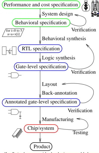
A modern design process (Figure 7) of a digital electronic system follows a more complicated design flow than the one in Figure 6. The specification is done at sev-eral levels: performance and cost specification saying what a customer wants and can afford, behavioral specification usually in some high-level specification lan-guages describing the desired behavior (algorithm) of the system. Then comes
val-idation of the specification. Usually it is very difficult to verify performance and
cost, but at least some properties of the functionality can be checked. Then the architecture and the interfaces are defined. The behavioral specification is trans-formed into a feasible-to-manufacture specification by synthesis, either manual, or partially or fully automated.
The current state-of-the-art automated synthesis proceeds in two steps, because algorithms and computational power which could do it in one step are not avail-able. First the behavioral specification is transformed into a register transfer level specification (RTL) in a process called behavioral synthesis. Then this RTL model is transformed into a gate-level specification. This process is called logic synthesis.
Excluding possible implementa-tions of our original specifica-tion in terms of a mechanical, analog, or in the future optical or even quantum systems, there are many gate-level systems sat-isfying the behavioral specifica-tion. Which one to choose is a sub-task of synthesis called
design-space exploration.
Unless an ideal synthesis tool is used, the gate-level description must be verified against the cus-tomer’s or at least the behavioral specification. Once we have a satisfactory gate-level specifica-tion expressed as an oriented multi-graph (nodes are gates, edges are interconnections, the orientation is input to output), it is transformed into a multi-level
planar graph in a process called layout. Library cells are placed on what will become an IC chip, and interconnections are routed. The layout, also called
place & route task, must produce something that chip manufacturers (called found-ries) can physically produce at a price acceptable to the customer. Apart from
fea-FIGURE 7: Design flow
Performance and cost specification
Behavioral specification Behavioral synthesis RTL specification Logic synthesis Gate-level specification Layout Back-annotation Verification Manufacturing Testing Verification Verification System design
Annotated gate-level specification
Chip/system
Product
If all tools were ideal, design would be a straightforward, not iterative process. Bugs found during verification return us one or more levels up.
for i=0 to 5 a=a+x[i]
ture-line width there are many other limits on the geometry of a physical design
such as the distances between wires, the shape of corners, etc., called design rules. Layout is always driven by design rules and a design rule check (DRC) is done after layout. Then the physical specification is verified as an analog circuit or more frequently as an annotated gate-level design. At this point in the design flow we can for the first time accurately verify timing (i.e., performance) and the consumed power. The foundry manufactures the circuits producing silicon, GaAs or other semiconductor chips, or multi-chip modules. Those are tested for structural defects relative to the gate-level netlist (structural faults) rather than for its function which is too costly.
The design flow is an iterative process. If verification at any stage identifies an error (a difference between the current and the higher-level specification), the designer or the automated tool returns to the previous step and chooses a different solution in the design space exploration. If no solution leading to a satisfiable design is found, it simply means that the specification is incompatible with the cur-rent technology and algorithms. For example, an 80-bit floating point unit with throughput of 1TFlops on 0.01 mm2of silicon and under $1M is impossible now, but might be easy in 10 years. The problem of convergence of the design flow has become a hot topic in 1990-ties. The current logic delay-centric design flow needs too many iterations in deep submicron design (DSM) where interconnect delays are dominant over logic delays. Similar problems exists with power consumptions. The future probably belongs to synthesis tools that consider physical implementa-tion early in the design flow and optimize for delay, power, and area at the same time [BrOt98].
We shall be mainly concerned with synchronous digital CMOS circuits. The rea-son is that it is the prevailing technology today and in the near future. Our models are intended to be generic, but when technology details are introduced, then CMOS is assumed. In the next section we look in detail at what verification is, and what the problems and the possible solutions are.
1-2. Verification of electronic circuits
Verification is a process of confirming certain properties on the subject of the
investigation, a circuit in our case. In this section we see how verification can be classified and we look in detail at functional, timing, and power consumption veri-fication.
1-2.1 Classification of verification methods
Verification methods for electronic digital circuits can be classified either by the properties they check, or by the circuit description they work with, or by the approach they take, as summarized in Table I.
1-2.1.1 Functional verification
Functional verification checks the function of the design. For example, a multiplier should perform function c=a*b for any allowed values of inputs a and b. Note that it is not really important what the design is, whether a C-language code, an RTL structure, transistor-level description, a chip sitting on a testbench, or a human with a pencil and a piece of paper. The design is correct, if it is doing what the cus-tomer wants. But how can one specify what the cuscus-tomer wants? Usually by a
TABLE I: Classification of verification methods
Criteria of classification Property to verify Level of circuit
description Approach Possibili-ties according to the clas-sification criterion
Function Behavioral Simulation
Testability RTL Formal
Timing Gate
Consumed power Switch Transistor
high-level description, such as our behavioral c=a*b or few test cases, e.g. “please, design a multiplier that computes 2*3=6 and 6*8=48, I don’t care about the rest.”
Design is usually done in hierarchical steps from the behavioral specification down to a network of transistors. Verification can thus be done in each step too to discover problems as early as possible.
A design is considered cor-rect, if the new synthesized lower-level specification
implies the higher-level one.
The “implication” is used in the sense “[the design] does everything and maybe more”.
That “more” are the internal signals, intermediate states, etc. The implication is transitive, so the chain of implications from the transistor down to the behavioral level is the same as a direct implication. That would be the ideal case. In reality, many specifications are not complete [CerK95], making checking whether one design completely implies another one impossible. The methods of functional ver-ification are discussed in detail in Section 1-2.1.11 on page 15.
1-2.1.2 Testability
Once a circuit is physically manufactured, it must be tested. Testing can be very costly. An average ASIC/FPGA/memory tester costs around $1M (or $5k per channel), plus the cost of developing testbench programs, and the cost of the time spent by testing. Also, some circuits are easier to test than others. To save money, to increase reliability, and to speed up testing, designers employ design for
test-ability (DFT). It is a collection of design methods, which either add some circuitry
(such as BIST, build-in self test), or use different implementations such as ones not having undetectable faults. Testability is beyond the scope of this thesis, however.
FIGURE 8: Task of formal verification
Multiplier complete Implementation Is specification Implies
?
?
specification⇐
2*3=6 6*8=481-2.1.3 Timing verification
The performance of electronic products is often the major selling point. People upgrade computers after only few years of service, doubling the performance. Anybody can say that it is the new features and the functionality of the many soft-ware products that make it sell - but the features are enabled by the higher perfor-mance in all senses of that word. One of them is the raw speed expressed in either MHz, MIPS, SPECint or some better application-specific units.
Verification of timing properties of digital circuits is necessary either to find out whether a circuit meets the timing specification (like the system’s clock frequency) or to inquire about the current performance of the system (the maximum clock fre-quency that may be applied). Timing verification is introduced in detail in Section 1-2.2 on page 17.
1-2.1.4 Verification of power consumption
With the diminishing physical dimensions and the need for portable electronic products with long battery life, the amount of power consumed by the products is more and more important. The average power drawn by circuits determines the duration of independent stand-alone use, or the dimensions and the weight of the batteries.
Another reason for the verification of power consumption is the functional correct-ness of the device with respect to the used technologies. The average power (to be defined later) consumed by a circuit should not exceed the maximum power the package is capable to dissipate, otherwise there is a danger of overheating. High peak power can cause voltage drops in power supply lines, leaving the circuit as if the power supply failed. Verification of power consumption is discussed in detail in Section 1-2.3 on page 20.
Next we shall see how different is the verification of a circuit described at the behavioral-level, RTL, gate or transistor level. Each has some advantages as well as disadvantages.
1-2.1.5 Verification properties on a behavioral model
A behavioral model of a circuit or a system is noth-ing but pure functionality, sometimes augmented with basic system requirements such as overall speed, power consumption and cost. Such a description is usually written in a formal language
(like that shown in Figure 9) based on the original description in plain English. E.g., “I want a SCSI-III interface with tag queue size of 32” means for a system designer to read through the SCSI-III standard definition and capture it in a formal language such as C++ or VHDL. There is no way to check whether he/she cap-tured it correctly, but he/she can still verify many properties of his/her behavioral model1. It can be, e.g., that no SCSI command is lost, or that the controller per-forms basic operations when connected to a behavioral model of a disk and that of a computer. The latter approach of trying few possible cases is called simulation [SaVi81, Pede84], the former (proving that no command can ever be lost) may be easier to achieve by formal methods [Schr97], we shall discuss both in Sections 1-2.1.10 and 1-2.1.11. No matter what approach is taken, the functionality can be checked using a behavioral description of the system.
Functionality of smaller blocks is easier to verify, but one should not forget to ver-ify the compatibility of interfaces between partitions, compliance of behavior of each partition with the interface specification, compatibility of interfaces each with other, as well as realizability of interface specification [CerK95].
1. Model versus description: generally when talking about manufacturing, “description” is what specifies what to manufacture; “model” is referred to what is necessary to verify (sim-ulate) what will be manufactured based on the “description.” In a modern design flow, veri-fication and manufacturing are closely coupled; therefore, “description” and “model” are considered synonymous in this thesis.
FIGURE 9: Behavioral description
for (i=0; i<10; i++) k[i+1] = k[i]*l + v
Functionality can be checked at the behavioral level. How about performance and consumed power? Some estimates1are possible, but more often they impose con-straints on the partitions of the system which are passed to behavioral synthesis. They can be left blank, i.e., we build a system and then see how good it is. Such an approach was common and acceptable in the early years of electronic design but not any more.
1-2.1.6 Verification of an RTL description
Behavioral synthesis, either manual or automated, translates a behavioral description into an RTL description under timing, power, and cost (area) constraints. An RTL description is similar to a behavioral one in the sense that it operates with
objects at a higher level of abstraction, such as integers, enumerated types, some-times floating-point numbers, and Booleans. However, the function is described by register transfers as the acronym RTL indicates. Each data type is assigned a fixed length in bits; the width of the data-paths, pipelines, how many functional units and how interconnected they are, all that is known. An example of RTL description is shown in Figure 10.
Functionality of an RTL description (model) is verified by either checking some properties of individual cases, or by checking that the whole RTL implies the behavioral model. E.g., the behavior of a multiplier is c=a*b, its implementation can be a 4-stage pipeline with 1000 bits of registers. We have to show that no mat-ter in what order and what numbers are fed into the multiplier, it still holds that 4 clock cycles after the inputs a, b are entered at time t the result is a*b, i.e.,
c[t+4]=a[t]*b[t]. But it is not the same as the un-timed model c=a*b, which we
1. Verification versus estimates: it will be seen later in Section 2-2 on page 40 that some verifi-cation methods are capable of computing estimates, others are exact; estimates are easier to obtain, so in many parts of this introduction we encounter sentences like “at the gate level, estimation of power consumption is possible”
FIGURE 10: RTL description 32
32
read as c[t]=a[t]*b[t]! Yes, they are different, it actually means that also the other components (e.g., the unit that generates data for the multiplier, or the unit that uses its output) must be pipelined. If they are not or are pipelined with a different number of stages, a stall logic or buffers must be added … and verified. How to verify such additions (called glue logic) precisely without building an RTL model of the whole system is beyond the scope of this thesis as well as the knowledge of the author.
An RTL model defines what data, how, and when moves around in the circuit. Having a good library of generic RTL building blocks with estimates on delay and consumed power, one can make very good predictions or optimizations based on performance (system clock), cost (number of units, i.e., area), and recently also consumed power. Yet, an RTL model alone is not sufficient to estimate consumed power as will be seen later in Section 1-2.3 on page 20, some information on input data is needed too. After design space exploration, the most promising RTL design is the input to logic synthesis. Logic synthesis produces a gate level description, which allows us to verify many interesting properties as outlined in the following section.
1-2.1.7 Verification at the gate level
Logic synthesis translates an RTL description into a gate-level description (model). Generic components such as adders of an arbitrary width are expressed as networks of gates (Figure 11). Gate-level models reflect
exactly the Boolean equations that implement each synthesized block. Functional-ity may again be verified against a higher-level description. But the gate level rep-resentation is more accurate for computing test vectors (and eventually fault coverage), timing errors, cost, and power consumption estimation.
Since gates are generally the smallest units (cells) in the library, the timing infor-mation and other electrical characteristics can be precisely captured. Knowing how
FIGURE 11: Gate-level description
a gate is interconnected with other gates allows to estimate the propagation time through the gate and the slew degradation on output signals. The delays on inter-connections are not known yet, however, because the length and the spatial distri-bution of interconnections are not known. Till about early 1990s, the
interconnection delays were neglected. Now, with higher integration (smaller
gates, but more of them) the interconnect delay is changing from nearly negligible to the dominant delay in a circuit.
Power consumption can be estimated quite accurately at the gate level. As will be explained later in Section 2-1.9 on page 38, transitions, i.e., changes in the Bool-ean value of a signal, are the major cause of power consumption in CMOS gates. Knowing the input signals, their timing, and the paths along which the input transi-tion will propagate, it is possible to estimate the power consumptransi-tion reasonably well. More accurate estimates are possible at the transistor level as shown in the following two sections.
1-2.1.8 Verification at the transistor level
Technology mapping is a process of mapping a gate
level description onto a particular technology library which is usually specific to each foundry. Many large design companies build their own librar-ies to reduce the dependence on foundrlibrar-ies. The result of technology mapping is a transistor-level description. A transistor-level model views digital gates as an analog circuit, e.g., the circuit in
Figure 12 is a two-input CMOS technology AND gate. Analysis of the analog cir-cuit can discover many problems in driving strength, timing, parasitic capacitance, resistance, and inductance. Yet, when working with some synthesis tools, there is no visible transistor-level description. The reason is that the RTL is mapped onto individual cells, that have functionality of less than one, one, or more gates. The foundry (owner of the library) provides only the names of the cells and many
FIGURE 12: Transistor level
parameters, such as area, timing information, power consumption indication, etc. The cell implementation is not public, neither is its layout (mask description).
Individual cells are always analyzed at the transistor level to assure functionality and to extract timing, power, and other electrical parameters. The process is called
cell characterization, see e.g., [ChoS95]. The extracted parameters are exactly
what the library vendor provides to designers and some more proprietary data such as the variations of the parameters due to the imperfections in the manufacturing process. Whenever needed the whole circuit or a block may have to be verified at the transistor level. This is the case when the cell library is inaccurate for the clock frequency used, incompletely characterized, or a special design is used, such as
dynamic logic. (Any combinational transistor level circuit shown in this thesis will
be static CMOS logic - it does not require any clock signal for its operation unlike dynamic logic [GoMa83]).
The enormous size of a transistor-level description for even a small circuit encour-ages the development of hybrid models - close to transistor-level in accuracy, yet benefiting from the gate-level model simplicity. Therefore, switch-level models and piece-wise linear signal representations have been introduced [Bryb87]. We can see the same phenomenon happening in verification at every level of abstrac-tion - the engineers want to get the accuracy of lower levels with the lower com-plexity of the higher levels of abstraction.
What is missing for accurate timing and power consumption verification at the transistor level is the knowledge of interconnects, and thus the incurred capacitive load. Since the cell placement is not known, the crosstalk (coupling) between interconnections is not known either. Excluding the mask library for the individual cells, many electrical parameters become known only after layout, which we dis-cuss next.