HAL Id: tel-00364546
https://tel.archives-ouvertes.fr/tel-00364546
Submitted on 26 Feb 2009HAL is a multi-disciplinary open access archive for the deposit and dissemination of sci-entific research documents, whether they are pub-lished or not. The documents may come from teaching and research institutions in France or abroad, or from public or private research centers.
L’archive ouverte pluridisciplinaire HAL, est destinée au dépôt et à la diffusion de documents scientifiques de niveau recherche, publiés ou non, émanant des établissements d’enseignement et de recherche français ou étrangers, des laboratoires publics ou privés.
Test a Complete Set of ADCs and DACs Embedded in a
Complex SiP or SoC
Vincent Kerzérho
To cite this version:
Vincent Kerzérho. ”Analogue Network of Converters”: a DfT Technique to Test a Complete Set of ADCs and DACs Embedded in a Complex SiP or SoC. Sciences de l’ingénieur [physics]. Université Montpellier II - Sciences et Techniques du Languedoc, 2008. Français. �tel-00364546�
UNIVERSITÉ MONTPELLIER II
SCIENCES ET TECHNIQUES DU LANGUEDOC
THÈSEPour obtenir le grade de
DOCTEUR DE L’UNIVERSITÉ DE MONTPELLIER II
Discipline : Systèmes Automatiques et Microélectroniques Ecole doctorale : Information, Structures et Systèmes
Présentée et soutenue publiquement Par
Vincent KERZÉRHO
Le 22 avril 2008Titre :
“Analogue Network of Converters”:
a DfT Technique to Test a Complete Set
of ADCs and DACs Embedded in a
Complex SiP or SoC
Jose-Luis Huertas Professeur Universidad de Sevilla, Espagne Rapporteur Pascal Fouillat Professeur Univ. Bordeaux I/ IMS Rapporteur Michel Renovell Directeur de recherche CNRS/ LIRMM Directeur de thèse Philippe Cauvet Test manager NXP Caen Examinateur Serge Bernard Chargé de recherche CNRS/LIRMM Examinateur Mariane Comte Maitre de conférences UM2/LIRMM Examinateur Florence Azais Chargée de recherche CNRS/LIRMM Examinateur Dominique Dallet Professeur Univ. Bordeaux I/ IMS Examinateur
La science est toujours utile, On ne perd pas le temps employé à l’acquérir [proverbe chinois]
Remerciements (Acknowledgements )
Mes remerciements vont tout d’abord à Jose-Luis Huertas, professeur à
l’université de Séville et Pascal Fouillard, professeur à l’université de
Bordeaux I pour avoir porté de l’intérêt à mes travaux et accepté d’être
les rapporteurs de ce mémoire de thèse.
Merci à Michel Renovell qui a été un directeur de thèse disponible et
accessible.
Je souhaite remercier Philippe Cauvet et Serge Bernard pour leur
encadrement qui a permis de montrer qu’il est possible de réaliser une
thèse entre un laboratoire et une entreprise et de fournir des résultats qui
contentent les deux parties.
Ce travail n’aurait pu être réalisé sans le soutien de Serge, Philippe,
Michel, Mariane, Florence merci d’avoir été là chaque fois que j’avais
besoin de votre expérience et de votre jugement d’expertise surtout pour
mes présentations.
Il me tient à coeur de remercier tous les employés de NXP qui ont
supporté mes intrusions intempestives dans leurs services et laboratoire :
Philippe, Gilles, Stéphane, Laton... La liste est trop longue pour être
exhaustive.
Je tiens à remercier Omar Chakib stagiaire Master. Il a su en peu de
temps s’imprégner de mes travaux afin de réaliser un stage qui m’a été
très utile pour terminer dans les temps.
Je voudrais exprimer ma reconnaissance à mes collègues et amis
thésards, prestataires de services, stagiaires, sans-emploi ou nouvellement
embauché : Bogu, Nanath, Laton, Georgi, Mag, Zioud, Elise, Estelle, La
Mercier Family, LeCatu. Ils ont été tout simplement présents à tous les
moments, aussi bien dans les moments de joie, de pression, de
décompression que dans les moments difficiles tout au long de ces trois
années.
Je souhaite exprimer mon amitié à Réouven, Boris, Waël, merci de me
supporter depuis si longtemps maintenant.
Merci à mes parents Nadine et Alain, ainsi qu’à mon frère Pierre-Marie,
pour avoir cru en moi et m’avoir poussé depuis toujours.
Enfin je remercie Anne-Laure et Mayeul pour les instants de bonheur
qu’ils me donnent le jour comme la nuit et qui m’aident à aller de l’avant
This work has been carried out within the framework of
IsyTest (Institute for System Testing) a joint institute between
NXP and LIRMM and under the umbrella of the European
MEDEA+ Project: "Nanotest".
Chapter 1 Context and state-of-the-art ... 1-1
I Context ... 1-2 I.1 Introduction... 1-2 I.2 Systems development trends... 1-2
I.2.A Increasing system complexity... 1-2 I.2.B Increasing hardware integration rate... 1-5 I.3 Test issues ... 1-11
I.3.A Analogue test strategy issue... 1-11 I.3.B Test platform issues ... 1-11 I.4 Summary and objectives ... 1-12 II State-of-the-art of system-level testing... 1-15
II.1 Introduction... 1-15 II.2 Signal path in systems to transfer from core-level to system-level testing 1-15
II.3 Configurations for system-level testing ... 1-17 II.3.A Introduction... 1-17 II.3.B An example: system-level testing for transceivers ... 1-18
II.3.B.a. System-level testing of transceivers: error-vector-magnitude ... 1-18 II.3.B.b. System-level testing of transceivers: Bit-error-rate... 1-21 II.3.B.c. Hardware implementation of system-level testing of transceivers: path-based ... 1-22 II.3.B.d. Hardware implementation of system-level testing for transceivers: Loopback-based implementation ... 1-22 II.3.B.e. Alternate methods ... 1-28 II.4 Conclusion ... 1-32
Chapter 2 Fully digital method to test a set of DACs and ADCs embedded in a complex system ... 2-1
I Introduction... 2-2 II Basics of converter testing... 2-2
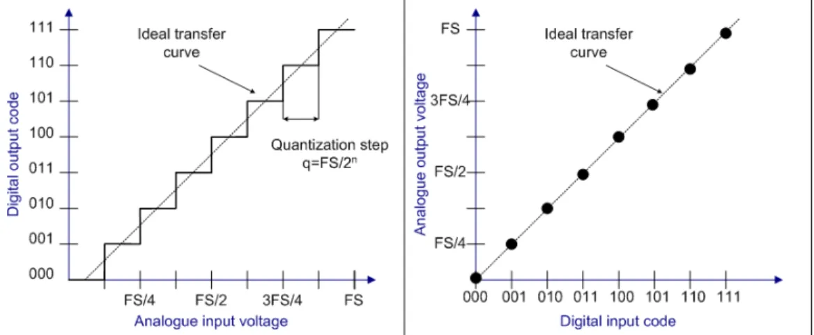
II.1 Introduction... 2-2 II.2 Errors affecting converters... 2-5
II.2.A Deterministic errors ... 2-5 II.2.B Stochastic errors... 2-8 II.3 Converter test parameters ... 2-9
II.3.A Static parameters... 2-9 II.3.B Dynamic parameters ... 2-10 II.4 Converters testing ... 2-13
II.4.A Usual test set-up... 2-13 II.4.B Test methods ... 2-14
II.4.B.a. Static testing... 2-14 II.4.B.b. Dynamic testing... 2-14 II.5 Summary ... 2-14 III State-of-the-art of fully digital test methods for converters... 2-15
III.1 Introduction... 2-15 III.2 Built-In-Self-Test (BIST)... 2-15 III.2.A Histogram-based BIST... 2-15
Table of contents
III.2.B Oscillation-based BIST... 2-16 III.2.C FFT-based BIST... 2-18 III.3 Functional elements as test instruments... 2-18 III.3.A Re-use of embedded functional DAC to test ADC... 2-19 III.3.B DAC/ADC chain, test of both elements simultaneously ... 2-19 III.3.C DAC/ADC chain, discrimination of test parameters of both elements 2-19
III.4 Summary and opening ... 2-22 IV Serialization of DACs and ADCs in complex systems in order to test them ………...2-23
IV.1 Introduction... 2-23 IV.2 DAC/ADC chain test difficulties ... 2-26 IV.2.A One converter model... 2-26 IV.2.B DAC/ADC chain model... 2-31 IV.3 Conclusion and opening... 2-33 V Method to discriminate harmonic contributions of interconnected
converters... 2-34 V.1 Introduction to Analogue Network of Converters ... 2-34 V.2 Two DACs and one ADC ... 2-36 V.2.A Configuration C(1,1) at full-scale ... 2-36 V.2.B Configuration C(2,1) at full-scale ... 2-38 V.2.C Configuration C(1,1) and C(2,1) at half -scale ... 2-40 V.3 Generalization ... 2-43
V.3.A Basic principle ... 2-43 V.3.B Generalization example ... 2-44 VI Conclusion ... 2-46
Chapter 3 Validation of the ANC-based method... 3-1
I Introduction... 3-2 II Simulation results... 3-2
II.1 Converter model... 3-2 II.1.A Sampling jitter... 3-3 II.1.B Thermal noise... 3-4 II.1.C Non-linearity ... 3-4 II.1.D Final model ... 3-6 II.2 Simulation setup and strategy ... 3-6 II.3 Test method efficiency... 3-8
II.3.A Validation on several samples of converters ... 3-8 II.3.B Study of the test method sensitivity ... 3-9 II.3.C Quantitative estimation of acceptable amount of noise ... 3-14 II.4 Application field of the proposed method ... 3-18 II.5 Summary ... 3-21 III Hardware measurement results... 3-21
III.1 Validation setup ... 3-22 III.2 Results and discussion ... 3-26 III.2.A Splitter influence characterization ... 3-26 III.2.B ANC method experimental validation ... 3-27 III.2.B.a. Test of three converters using ANC method ... 3-27
III.2.B.b. Learning and test production steps validation... 3-28 IV Conclusion ... 3-29
Chapter 4 Extension of the application field of the ANC method... 4-1
I Introduction... 4-2 II ADC testing with low resolution Arbitrary Waveform Generators ... 4-2
II.1 Introduction... 4-2 II.2 Influence of AWG on the Test quality... 4-3
II.2.A Noise level ... 4-3 II.2.B Harmonic distortions... 4-4 II.2.C Conclusion ... 4-5 II.3 State-of-the-art of ADC test methods using low performance analogue signal generators ... 4-5
II.3.A SEIR method... 4-5 II.3.B 2-ADC method... 4-6 II.3.C Summary ... 4-7 II.4 A new solution to test ADC dynamic parameters using low-resolution
AWG 4-7
II.4.A ANC-based alternative method for production test of ADC ... 4-7 II.4.A.a. Theoretical fundamentals ... 4-7 II.4.A.b. Learning AWG harmonic contribution for post-processing
calibration ... 4-8 II.4.A.c. Mass production test using post-processing calibration ... 4-10 II.4.B Hardware experimental validation... 4-11
II.4.B.a. Experimental set-up ... 4-11 II.4.B.b. Experimental protocol ... 4-12 II.4.B.c. Experimental results of the full test procedure ... 4-13 II.4.C Estimation of the production test efficiency vs. AWG resolution 4-15 II.4.C.a. Experimental protocol... 4-15 II.4.C.b. Experimental results ... 4-15 II.5 Conclusion ... 4-16 III Alternate DAC test, relaxing constraints on digitizer performances.4-17
III.1 Introduction... 4-17 III.2 Learning process ... 4-17 III.3 Mass test production ... 4-18 IV Self calibration of ATE ... 4-18 V Conclusion ... 4-19
Discussion and conclusion ... 5-1 References ... 6-1 Related publications ... 6-10 List of acronyms ... 6-11 List of figures ... 6-12 List of tables ... 6-15
Table of contents
I
ntroduction
The conventional approach to test analogue/RF systems is to test each component separately. The methods developed to test these components are matured and effective considering that the system is made of physically independent elements, because we need to access the primary inputs and outputs of the components. Another required condition is the use of analogue instruments with better performances than the component under test ones. For instance, it is commonly admitted that to test a N-bit ADC, there is a need of at least a N+2-bit analogue waveform generator.
The trends for system design make difficult to match all these required conditions. Indeed due to an increasing integration rate it becomes difficult to access primary inputs and outputs of components under test. In addition it becomes difficult to find effective analogue test instruments. Chap.1 describes precisely these trends for system design and gives the resulting test issues. A new trend in test development consists in addressing the test at a system-level and not anymore at a core-level. A state-of-the-art of the test methods dealing with these test constraints is also given.
Considering all these promising test approaches at a system-level, it usually appears that integrated Digital-to-Analogue Converters (DAC) and Analogue-to-Digital Converters (ADC) are respectively used as stimuli generators and test response digitizers. In order to enable the use of integrated converters for a test purpose, they should be firstly tested to insure their quality and effectiveness. The second chapter is dedicated to a new test method that we have developed. This method is called ANC-based method and has been developed to test a set of Analogue-to-Digital Converters (ADC) and Digital-to-Analogue Converters (DAC) embedded in a complex system such as a SiP or a SoC. The ANC-based method has been developed considering previously given test issues relative to system design trends.
The purpose of the third chapter is to validate the theoretical developments previously described by evaluating the efficiency of the ANC-based test method. The efficiency will be considered in terms of accuracy for the estimation of some dynamic parameters according to converter resolutions and performances. The validation is conducted in two steps: simulation and hardware measurement.
The test method is suited to test a set of converters embedded in a complex system. It has been developed for a general case considering the converter architectures and resolutions and the number of converters under test. As a consequence the domain of application of the method has been extended to the test of stand-alone ADCs and DACs and to the calibration of analogue instruments. Finally, the proposed method is extended in the fourth chapter to a larger application field including stand-alone ADCs and DACs, as well as the calibrationof analogue instruments.
1-1
Chapter 1
Chapter 1: context and state-of-the-art
I
Context
I.1 Introduction
Nowadays microsystems find applications in many domains. Indeed microsystems are used in consumer applications but also non-exhaustively in automotive, space, and healthcare applications. These different domains tend to drive microsystems development in many directions, considering different purposes, and consequently inducing a lot of challenges. This first part of the chapter presents an overview of the development trends for systems, and the related test issues.
I.2 Systems development trends I.2.A Increasing system complexity
A complex system is usually made of heterogeneous components, in other words components made in various technologies and consequently working in different domains, such as RF, mixed-signal or digital ones. A high-level complexity is reached when the system works in the three domains. We find such complex systems in mass production applications like cell phones, WLAN transceivers, digital TV receivers, near-field communication devices, automotive electronic products, but also in specific application fields such as instrumentation, industrial, and aerospace. In wireless applications, the system architecture is traditionally divided into an RF front-end transceiver and a base-band section. They are interfaced with analogue-to-digital converters (ADC) and digital-to-analogue converters (DAC).
Increasing system complexity is driven by the trend in offering more and more services with one product. The best example of this service integration trend is the cell phone. Indeed a current cell phone offers a huge number of services. These services can be classified in two categories: hardware and software services. Following tables give a non-exhaustive list of current and future services.
Hardware services Software services
Digital TV reception Voice/Image recording Wireless Bluetooth communication for
headset SMS
Wi-Fi communication for internet connection
Games
Compass Mp3 player
Sensors for camera and video camera Polyphonic rings
Organizer Table 1-1: Current cell phone services
1-3
Hardware services Software services
Health monitoring Distant learning/ home office
Defibrillator More secured services
GPS e-education
Context awareness e-commerce
Location based services (news, maps…) Table 1-2: Future cell phone services
According to the example of cell phones, it is obvious that the multiple services available with actual complex systems push towards the developments of RF, mixed-signal and digital components.
Higher bandwidth is obviously a dominant driver to more RF applications development. It is pushed by the combined development of increasing internet use, the growing size of transferred files and increased bandwidth of wired connections. Indeed nowadays communication standards are USB2, Firewire or gigabit Ethernet connections, that offer bit rates over 200Mb/s. Figure 1-1 gives a chronological description of the evolution of frequencies used for RF application.
Figure 1-1: Chronological evolution of RF application frequencies [hooi03] Chronologically, the first RF application was AM radio. It is also the first RF broadcasting application. Following RF broadcasting applications were Frequency Modulation (FM) radio (87.5-108.5MHz), developed by Edwin H. Armstrong in 1933, TV very high frequency or VHF (174-230MHz), TV ultra high frequency or UHF (470-860MHz). Once analogue modulation limits has been reached, thanks to digital modulation and satellite communication, a next step has been overcame. Indeed nowadays standards use gigahertz frequencies. Future RF broadcasting would be done at 20 or 30 GHz.
Chapter 1: context and state-of-the-art
The second application of RF transmission is mobile telephone. On contrary to broadcasting applications, mobile phone applications had a very fast development. In only 10 years from 1990 and 2000, it has reached a high-level integration rate and has flooded the market. The first generation was using 900MHz band. Currently, the mobile phones of the third generation (Ultra mobile communication system UMTS) use the 2GHz band. Future generations would work at 40GHz.
The third RF application, Wireless Local Area Network (LAN) and Personal Area Network (PAN) have emerged from the success of mobile phone, internet and need of wireless broadband internet access. This is the third application to RF communications, nowadays using the 2.4-2.5GHz bands, and over 10GHz in the future.
Because of increasing frequencies, some parasitic elements become dominant. Layout elements that could be ignored become non-negligible and influence circuit performances [hooi03]. Some of these new contributive elements are interconnections such as bond pads, bumps. Consequently, the test of these components becomes a real challenge.
Complex systems tend also to integrate more mixed-signal components such as analogue-to-digital and digital-to-analogue converters, with increasing resolution and frequencies. The resolution is depending on the quality requirements of the signals coming from or sourced to the RF section [mirf07]. In addition to the improvement of their performances, the number of data converters is growing in integrated systems. The following figure gives an example of a complex system embedding several data converters. The product is the NXP pnx8327 type, a digital television decoder system. Apart from RF and digital components, it embeds 2 ADCs and 6 DACs.
Figure 1-2: NXP pnx8327, digital TV receiver for set-top box application The functional frequency race is not only the spearhead of personal computer processor manufacturers. Indeed, as previously mentioned, complex systems propose an increasing number of services in one product. Those services are not only hardware-based new functionalities. But they are in majority software services proposing image or sound processing, or multi-media applications. This demand drives the development of the digital functions in the systems, with key factors such as the clock rate, and the computational and storage capabilities. An example of such a complex system embedding a lot of digital elements is the Intel PXA800f, it is a cellular processor for wireless-internet-on-a-chip. Figure 1-3 gives an overview of the block diagram of the product. The digital part embeds four types of memory:
1-5 9 SDRAM stacked
9 Intel Flash stacked 9 Intel Flash
9 SRAM frame buffers
Additionally, this SoC includes a lot of computation units.
Figure 1-3: Intel pxa800f I.2.B Increasing hardware integration rate
Because of the high-volume nature of consumer products, cost reduction has always been a key factor of success for chips suppliers. As a consequence, the integration density is also increasing in parallel with the improvement of the system performances. Additionally, the reduction of the form factor represents a key advantage in portable applications [farl04], thanks to a decreasing number and to a size reduction of the components. Figure 1-4 illustrates the reduction of the number of components in a mobile. We can see that, as the cellular phone was flooding the market, the number of IC’s in the system decreased by a factor of 10, from 300 to 30.
Chapter 1: context and state-of-the-art
Figure 1-4: Chronological description of number of ICs in a cell phone / number of subscribers [bi01]
The desire for low off-chip component count in RF applications has led to the introduction of even more integrated RF front-ends, using architectures like zero-IF or near zero IF. Following Figure 1-5 gives an example of a typical block diagram of a direct conversion or zero-IF transceiver architecture. This architecture uses the now well-known IQ modulation. It is a hardware implementation of a rectangular to polar coordinate conversion. The transmitted signal will be of the form
( ) ( ) (
t I t cos2 ft) ( ) (
Q t sin2 f t)
s = π0 + π 0 eq. 1-1
where I(t) and Q(t) are the signals to transmit, digitally modulated. And f0 is the
carrier frequency. This IQ modulation gives a higher signal quality.
1-7
Figure 1-6 presents a superheterodyne architecture with an IQ modulation. The superheterodyne architecture is based on several frequency shifting. Each frequency shifting requires a mixer and a local oscillator. As a consequence the more you shift your frequency, the more you increase the number of required components.
Figure 1-6: Superheterodyne architecture
These two types of RF transceivers illustrate the trend towards a reduction of the number of analogue components, in other words to a digitization of the transceivers.
Indeed, pushed by the steady development of successive generations of CMOS technology, processing capabilities have become so high that complex functions like demodulation are now performed in the digital domain. Over the years the analogue-to-digital converter (ADC) in receivers has thus moved slowly towards the antenna. The whole digitization of analogue functions is actually limited by the power consumption of ADCs [hooi03].
The digitization for signal processing in RF applications and the increasing frequencies in the end-systems (cell phone, WLAN, Bluetooth…) have led to the introduction of a new concept, the software-defined radio (SDR). A SDR system is a radio communication system, which can tune to any frequency band and receive any modulation. In order to enable the adaptability of the system to several frequencies and modulations, significant amount of signal processing is transferred from analogue/RF to digital domain. As a consequence a new run for a new form of radio protocol consists in running new software.
Chapter 1: context and state-of-the-art
Figure 1-7: SDR architecture
The ideal SDR is made only of one antenna, some ADCs and DACs and a big computation unit. However, it cannot be really implemented yet, because of the limited bandwidth of the data converters.
The ultimate reduction of off-chip components is reached once we have only one package for the whole system. This final step can nowadays be reached using new technologies: SiP or SoC. As previously mentioned a complete system is made of digital, mixed-signal, analogue and RF components. Each component requires a particular technology. Thanks to recent technology developments, some solutions have been developed to embed all these components in only one package.
The SoC technology is created from a single chip, as a consequence a SoC is made using only one process technology. In addition it uses only one type of interconnections from the die to the package. The interconnection technologies used are wire bonding or flip chipping.
Figure 1-8: Example of SoC embedding, CFPA chip developed by CVAX. The second technology able to increase the density is the System-in-Package or SiP. Actually the SiP technology is not based on one solution, but various configurations are now available, using the stacked-die or the planar assembly, or both. A very attractive technology, named silicon-based SiP, has been developed for some years by NXP, based on two principles.
9 Stacking active dies on a passive one
1-9
Several different process technologies are used to fabricate the different dies (CMOS BiCMOS GaAs). In addition several interconnection levels are used between different dies, using several interconnect technologies (wire bond, flip chip, soldering, gluing).
Figure 1-9: Example of SiP made of two active dies stacked on a passive one Both SoC and SiP have advantages and drawbacks [wils05] [paill05] [cauv07]. Table 1-3 gives the pro’s and con’s for both technologies.
Chapter 1: context and state-of-the-art
For Against
Each functional die can be fabricated in his most suited technology
SiP technology uses some complex assembly processes that could
reduce reliability Possible plug-and-play approach, for example
considering an RF application system made of RF analogue mixed signal and digital dies, different RF designs can be done for different applications, without changing the baseband chip
SiP can be more compact thanks to high-q passive components and antenna integration. SiP
SiP design is shorter
Reliability not influenced by several complex assembly processes.
A SOC that contains 10 RF interfaces would be very sensitive to crosstalk
between inputs and to noise from digital
baseband
SoC fabrication is less expensive
It’s going to be very difficult to embed in one
chip all the future applications that would required in future systems,
like future cell phones. Suitable for mass production Increased design and test time. SoC
RF design are migrating from BiCMOS to CMOS as digital, it’s going to be possible to
propose a single chip solution
Table 1-3: For and against SiP and SoC
To summarize, the relatively short time to develop SiP devices makes the technology more appealing for consumer electronics that have short production cycles, and SiP is also growing fast in markets for WLAN, WiMAX, Bluetooth and Wi-Fi modules. Basically, SoC approach forces the supplier to a fixed solution for a long run, or for big volumes. An effective solution considering practical performances and cost could be to associate SiP and SoC, embedding SoC and other chips (saw filters, MEMS, power amplifiers, passive components) in a SiP [paill05] [cauv07].
System integration is challenging the edge of integrated systems and consequently affects the test. Indeed over last few years, test cost has been on the rise and nowadays constitutes a significant portion (up to 40%) of the total manufacturing cost for wireless products [bhat05]. As already seen, the trend is to integrate more and more applications and particularly RF applications. In parallel, the size and the price of these systems decrease. As a consequence test is driven by a constant trade-off between product test cost and test effectiveness. Increasing device complexity in terms of transistors count, frequencies, power consumption, and integration of diverse circuit types will pose significant challenges to the test community in the future.
1-11 I.3 Test issues
I.3.A Analogue test strategy issue
As digital components were growing up, the digital test strategy has been adapted. The first step was to define fault models such as stuck-at fault, in order to move test from a functional to a structural methodology. It consists of testing the structure of the digital component without taking into account the function emulated by the component. This structural test methodology permits to test a whole digital component embedding several functions using one test strategy. In addition to this translation from functional to structural methodology, the test development process benefits from automation. Indeed digital test synthesis and design for testability (DfT) tools have been developed to simplify the test development and optimize the test coverage. The digital test methodology follows the systems development trends.
In comparison to digital, mixed-signal and analogue test strategy is totally different [ozev04]. Actually, there is no efficient and simple fault model and no possible structural strategy. Consequently, the test methodology is not unique, and each core is tested independently using the results of a set of parametric measurements [DYNA00][Maho87][IEEE1241]. This strategy may be considered as a legacy, because, until recently, all the cores of a system were used as stand-alone components. This strategy is no longer efficient, because of the restricted access to embedded cores. Even if there were enough access points, the test of the whole system would be very expensive. Indeed it would require a long test time because each core should be tested independently.
I.3.B Test platform issues
Equipment cost, for a long time, dominates product test cost [ITRT03]. The trend towards more system functionality on a single die (SoC) or in a single package (SiP) brings closer digital, analogue, RF/microwave and mixed-signal devices. Ideally, a single platform solution that can test any application should be used. In real life, the number of instruments in a given test system is limited to the maximum capabilities of the tester, and most importantly by the cost of ownership of such a sophisticated equipment. In addition instrument designs for ATE are chasing ever-increasing test requirements, especially for arbitrary waveform generators (AWG) and digitizers. AWG and digitizers are commonly used to test analogue and mixed-signal components. They require higher linearity and speed than the device under test (DUT) in order to ensure the test quality. As a consequence integrated circuits (IC) suppliers work to produce the best components in term of linearity and speed, and the test platform supplier should have better performances on their analogue instruments, close to one generation in advance. The needs for multiplying the instruments, for improving their performances are expected to continue if no breakthrough is achieved, leading to a contradiction with the permanent pressure on test costs. Examples are usually reported where the test of the analogue cores in the system may represent up to 90% of the whole test effort while these analogue cores only represent 10% of the whole chip area [kerz06]. Three key factors actually affect the costs of the analogue cores testing:
1. The time for development: because the tests cannot be simulated in advance, the time for debug is much longer than for digital cores
Chapter 1: context and state-of-the-art
2. The cost of ownership of the analogue instruments: it includes the price itself, but also the cost of the calibration, and of the maintenance
3. The test time: in general, it is function of the target accuracy, and of the settling of the device
In addition to high cost of analogue options, there are some technology limiters to analogue tests. The bandwidth, the sampling rates of AWGs, the dynamic range for RF applications, the noise floor, and the ability to integrate some digital and analogue instruments.
Multi-site parallel test as well as concurrent test of all analogue functions could be a solution to reduce test time [ITRT03]. It requires multiple instruments with fast parallel execution of DSP test algorithms (FFTs etc). Parallel test has been used for many years to test memory and high volume digital devices but not to test mixed-signal devices, because additional analogue instruments would increase tester cost and reduce the benefits of parallel testing.
I.4 Summary and objectives
Integration is the global trend in system development whatever the purpose. By integration we mean service and hardware integration. Concerning service integration, systems’ developments tend to integrate more and more services in one system. The most significant example is the cell phone, which nowadays proposes, not only to be able to make a phone call, but also to take a picture, listen to music, play games, watch the television, access the world wide web and future services that would address healthcare, e-commerce, or positioning (GPS). Concerning hardware integration, complex systems embed several technologies from RF to digital. From an architectural point of view, complex systems’ hardware is more and more digitized. Digitization consists mainly in transferring signal processing from RF to digital domain. Driven by the digitisation of the electronic functions, the software-defined radio facilitates the introduction of multiple RF transceivers into the systems. From hardware integration point-of-view, systems’ developments tend to integrate in one package the whole system. The trend is indorsed by SiP and SoC technologies. Figure 1-10 shows a simplified block diagram of a potential complex system. It is made of two main digital cores that embed several sub-blocks, and several analogue cores. The converters interface digital with analogue cores or internal cores with I/O pins.
1-13
Figure 1-10: Block diagram of a potential system.
These development trends induce some test issues more or less addressed by recent test evolutions. Concerning digital, Figure 1-11 presents the test implementation of digital cores from the previous potential system (Figure 1-10).
Figure 1-11: Test of digital cores from potential system
Test concepts addressed a global test. Structural test and digital BIST avoid issues like the reduced number of access points and the increasing complexity of digital portions embedded in complex systems.
Concerning RF, analogue and mixed-signal cores of systems, Figure 1-12 gives a non-exhaustive representation of configurations and paths required to test the analogue cores of such a complex system (Figure 1-10)
Chapter 1: context and state-of-the-art
Figure 1-12: Test of analogue cores of a potential system
Test methodologies are not well suited to the issues induced by development trends. Indeed in majority analogue cores are tested independently, requiring the access to primary inputs and outputs. It goes against development trends that consist of more functions on less area and consequently with less access points. And finally it induces a long-test time and as a result high test cost. In addition conventional test methodologies require dedicated analogue test instruments. These instruments are cost-effective by their own, and consequently the ATE, required to test a SoC or a SiP, is expensive because it requires a complex configuration to test all the cores, from RF to digital.
Alternate methods are needed for analogue/RF. Main issues stand in huge numbers of tests, access points and instruments due to the traditional core-level test strategy. A solution could be, like for digital cores, to change the strategy from core to system level. Therefore, two main objectives must be targeted:
1. System-level testing, for reduction of the number of tests and of the access points
2. Low-cost ATE using, in other words, digital-only testers, to get rid of the expensive analogue instruments
The two targets are described in the next section. Figure 1-13 gives an example of test paths for analogue and digital cores, which enable a fully digital test strategy
1-15
Figure 1-13: Fully digital tests
II
State-of-the-art of system-level testing
II.1 Introduction
Testing heterogeneous integrated systems requires test platforms with high-performances (i.e. high cost) instruments, usually dedicated to test each kind of technologies embedded in the system under test. The cost of test operation, directly dependant on the test time, is also significant. Indeed the traditional test approach for analogue/RF systems is based on a per-core strategy. Because of the increasing hardware complexity, the total test time could lead to a prohibitive test cost. Additionally, with the new integration technologies like SiP or SoC the number of test points becomes insufficient.
Considering all these issues, an obvious solution is to develop the test strategy at a system-level and not anymore at core-level. By system-level test, we mean that the device-under-test is not anymore a core but a multi-core system. In this second section, a first system-level test strategy (developed by Ozev et al) is introduced. The third sub-section presents some other test methodologies for system-level testing. Finally, the last sub-section addresses the hardware implementation of system-level test strategy also called path-based testing and loopback. This sub-section also gives some description of alternate methods.
II.2 Signal path in systems to transfer from core-level to system-level testing A first approach of system-level testing was developed by Ozev et al [ozev01][ozev04]. Their methodology aims at solving some problems induced by systems’ developments, namely:
9 The lack of test automation concerning the analogue cores 9 The ”per-core” strategy
Chapter 1: context and state-of-the-art
To address all these crucial issues Ozev et al propose to transfer core-level tests to system-level using existing functional signal paths, in several steps. At first, they propose to define the test stimulus characteristics (amplitude, frequency, phase, DC level, noise floor, accuracy) relatively to the test path. The second step consists of classifying core-level tests at the system level. The transfer of the test from core to system level induces a new test path. As a consequence the tests are classified in three categories relatively to the characteristics of the new test path:
9 Untranslatable due to amplitude and frequency range deficiency 9 Untranslatable due to noise or inadequate accuracy
9 Directly translatable tests
The classification is achieved according to the availability of a test stimulus from one core to be driven through the other cores. Using this transfer scheme allows to improve the automation of test development for analogue cores and for system.
The first experimental validation has been achieved on a quite basic system, only made of analogue cores: a typical two-channel up-conversion path shown in Figure 1-14.
Figure 1-14: Mixed-signal up-conversion path
Fifteen over twenty-two tests have been transferred from core-level to system-level. In addition good fault coverage has been obtained.
The first experimental validation address only analogue cores. As already mentioned, complex systems embed not only analogue and RF cores, but also digital elements. To go further in their approach, Ozev et al [ozev04] present a seamless test of digital components in mixed-signal paths. This approach goes further in the path-based test developments. Indeed they include a digital filter in the path under test, usually made of analogue cores. Digital elements are tested targeting stuck-at fault default. It obviates the need of test point for internal cores. It also permits at-speed test. A two-tone sine wave is used to test the digital filter. The tones of the two-tone sine wave are chosen close together. Indeed as presented in Figure 1-15, the closer are the tones, the greater variety of patterns you have.
1-17
Figure 1-15: Two examples of two-tone sine waves
Ozev et al [ozev01] [ozev04] propose an interesting methodology to move from core-level to system-level testing, in order to carry out a path-based test. This methodology is very interesting because it requires no test access point. As a consequence the test is applied at the primary inputs and captured at the primary outputs. The limited observability and controllability have some drawbacks. At first some key tests, like DNL of DAC in the example of [ozev01] cannot be performed and logged because of frequency or amplitude deficiency. Moreover, the test coverage is actually linked to the noise level of the whole path. In [ozev04], the authors show how the noise level can affect the test coverage in an example. To go further the path-based test methodology also developed by Ozev et al suffer from test masking, but this subject will be addresses in another section. Another drawback, with respect to our initial objectives, is linked to the required test configuration. Indeed, their methods require using at least one RF signal generator (for Rx testing) and one signal analyser (for Tx testing). But obviously the association of analogue and digital cores in the test path appears to be a promising approach that would surely be developed in future works.
II.3 Configurations for system-level testing II.3.A Introduction
As previously mentioned, systems are becoming more and more complex (cf. Figure 1-8, Figure 1-9, Figure 1-10), with a significant impact on test. A strategy, which could solve all these test issues, would address the whole system in its complexity (digital, analogue and RF cores). Ideally, the resulting configuration would get rid of the RF/analogue options of the tester, in other words would make use of a digital-only ATE.
Chapter 1: context and state-of-the-art
Ozev et al (cf.I.2.B) have proposed a configuration to address the whole complexity of a system. However, their solution suffers from several drawbacks. For the time being, no methodology exists for testing complex systems with digital, analogue and RF cores all together, although we can find some methodologies in the literature where analogue systems made of several cores are tested as a path. The second sub-section focuses on system-level testing of RF transceivers, as described in the literature. The third section deals with the implementation of such methodologies and some alternate methods using diverse configurations.
II.3.B An example: system-level testing for transceivers
II.3.B.a. System-level testing of transceivers: error-vector-magnitude
IQ modulation (cf. 1.B.b) can be used as RF parametric data. These data are usually displayed on a complex plane. Figure 1-16 gives an example of an IQ complex plan representation and an error vector for a symbol. This vector represents the difference in amplitude and phase between the real and the ideal (reference) vector.
Figure 1-16: Error vector between reference vector and measured vector Following figures are complex plane representation of IQ sampled data. This representation enables the detection of faults affecting the modulated signal. Indeed for a known signal as a sine wave, the modulated signal captured at the output of the DUT should follow an expected representation, and a particular variation in the constellation can characterize a particular default. Following figures present some measured constellations for faulty and fault-free signals and for several digital modulations.
1-19
Figure 1-17: Constellation and spectrum of a ;/4DQPSK modulated sine wave at 21kHz, no distortion
Figure 1-18: Constellation and spectrum of a ;/4DQPSK modulated sine wave at 21kHz, with distortion
Figure 1-17 and Figure 1-18 are the IQ plane representation of a sine wave (21kHz) modulated by a ;/4DQPSK. For Figure 1-17 the signal is not deteriorated as for Figure 1-18 the signal is deteriorated by some distortions. The difference is visually notable and permits to discriminate a good from a defective device. Figure 1-19 and Figure 1-20 are similar figures but for a different modulation and at a different frequency. Note that the shape of constellation is linked to the type of modulation.
Chapter 1: context and state-of-the-art
Figure 1-19: Constellation and spectrum of a QPSK modulated sine wave at 4.096MHz, no distortion
Figure 1-20: Constellation and spectrum of a QPSK modulated sine wave at 4.096MHz, with distortion
The most common parametric test parameter resulting from IQ sampled data is the error-vector-magnitude. The EVM is a specification that determines the performance of the wireless system in terms of transmitted and received symbols corresponding to a digital modulation. The EVM measurement, according to literature, is commonly used for receiver [acar06] [hald05_3] [dabr04] and transmitter testing [acar06] [hald06] [dabr04].
Practically, the EVM calculation is given by eq. 1-2 [hald05_3].
² S ² S R N 1 EVM max N 1
∑
− = eq. 1-21-21 S= reference symbol in vector form (I+jQ),
Smax= outermost symbol in the constellation diagram,
N=number of symbol used for EVM computation.
Dabrowski [dabr04] uses the EVM metric for testing a CDMA transceiver. The efficiency of EVM test is discussed considering the detection of spot defaults that degrade gain and/or NF of the RF cores. In order to improve fault coverage and to address some fault that are not susceptible to EVM, Dabrowski proposes to complete the test set by an IP3 test.
In [acar06] it is demonstrated that EVM testing alone cannot provide sufficiently high fault coverage. Taking this issue into account, the authors propose an input stimulus and a test limit optimisation, based on the detection capability, the set-up complexity and the test time of each test. They finally recommend combining EVM and a set of system level specifications to ensure product quality. With respect to the stimuli, they propose to reduce the number of symbols from 320, the IEEE standard recommendation, to 20. The method is based on a learning technique. The 320 symbols are applied to a set of DUTs, and then the redundant symbols are removed, leading to a significantly shortened test time (in their example, from 1.3ms to 80µs). The test results are also improved using complementary tests, such as Zin and Zout,
instead of IIP3 or noise figure that are considered to be too costly and time-consuming tests.
Another optimized EVM test is presented in [hald05_3]. Halder et al focus on test implementation cost. For a path-based test of an RF receiver, the ATE must embed an RF transmitter with the appropriate digital modulation capability and higher performance and accuracy than the receiver under test. To get rid of such an expensive configuration, Halder et al propose to use a low cost RF generator and to set the EVM test using a multi-tone sine wave as test signal. To improve the efficiency of a test using a low performance set-up, a learning process is necessary. This learning process consists in applying the “full” test and the simplified test on a set of DUTs and to calculate a non-linear regression between the two set of results. In production, the regression functions are used to predict the performances of the DUT using the results of the simplified test. A similar methodology has been proposed [hald06] to test RF transmitter.
II.3.B.b. System-level testing of transceivers: Bit-error-rate
At system level, the quality of the modulation of a receiver or a transmitter can also be estimated using the bit-error-rate (BER) parameter [bhat05] [dabr04] [nowa01]. BER is a system specification that measures the erroneous bits received for a fixed number of bits transmitted. Next equation gives the expression of the BER calculation. Tx e N N BER= eq. 1-3
where Ne is the number of error bits and Ntx the number of bits transmitted.
This parameter is sensitive to jitter and distortion. It quantifies the ability of the system to receive error-free data, and reflects the quality of the communication medium.
Chapter 1: context and state-of-the-art
A major drawback of BER test is often the huge number of samples to be acquired to get the target accuracy. Bhattacharya et al [bhat05] propose a method to reduce the number of symbol required to achieve a BER test. The algorithm selectively rotates the transmitted symbols to increase the BER. Using some simulation models of the transceiver, and some non-linear regression functions, the true BER can be estimated thanks to the alternate BER test, in a short test time.
Dabrowski [dabr05] focuses on fault masking risks resulting from BER technique. As a consequence some physical defects can be more difficult to detect. To overcome this issue Dabrowski proposes to increase the sensitivity of the signal path under BER test, by controlling the SNR at the input or by using a baseband interferer.
II.3.B.c. Hardware implementation of system-level testing of transceivers: path-based
The two previous sub-sections introduce various methodologies that can be used to develop a test strategy at system-level. These different tests are based on two types of hardware implementation: the path-based and the loopback-based ones.
The path-based implementation deals with the whole chain of the receiver or the transmitter under test. It uses the primary inputs to feed the stimulus and the primary outputs to capture the response. This test implementation is shown in a number of publications [acar06][hald05_2][hald05_03][hald06][ozev01][ozev04]. As a key advantage, this approach does require neither internal access nor specific DfT (Design-for-Test). However, RF instruments are necessary, such as signal generators for receivers, and down-converters coupled to digitizers for transmitters.
II.3.B.d. Hardware implementation of system-level testing for transceivers: Loopback-based implementation
Loopback-based implementation is the extension of the path-based strategy for transceivers. As shown in Figure 1-21, the receiver is connected to the transmitter; creating the loop in the transceiver. This hardware implementation of the system-level testing is depicted in many publications [bhat04] [bhat05] [bhat06] [dabr03] [dabr04] [dabr05] [hald05] [heut99] [jarw95] [lupe03] [negr02] [negr06].
1-23
Figure 1-21: Basic principle of loopback-based test implementation
The biggest advantage of using such a test path is the reduction of the test instrumentation. Only digital channels are required because the test signal is generated on-chip or on-board, then converted by the embedded DAC(s). The response signal is converted by the embedded ADC(s) and is either internally or externally processed. Therefore, no high-end RF instruments are required, in other terms, a low-cost tester may be used for even complex transceivers.
Several authors have covered the loopback topic from a hardware perspective. Connecting the Tx to the Rx close to the antenna is not straightforward. Indeed, signals generated by the Tx and entering in a Rx have different frequencies and amplitudes in the application context.
Yoon and Eisenstadt have designed a loopback for 5-GHz WLAN transceiver [yoon05]. The proposed approach explores the on-chip implementation of the loopback. The following figure gives the core diagram the configuration.
Chapter 1: context and state-of-the-art
Figure 1-22: Core diagram of a loopback implementation for WLAN transceiver [yoon05]
Due to on-chip implementation of the loopback, the band-pass filter, close to the antenna, and the high power amplifier in the transmission path are removed for testing. In this application, there is no need for frequency shifting. Therefore, the loopback subcircuits are high-frequency attenuators, which reduce the transmitted signal to sufficiently low signal amplitudes, and RF switches that select the test path operation or normal operation signal path.
The purpose of [yoon05] is to design and evaluate a loopback, taking some performance and surface constraints into consideration. Several types of attenuator and RF switches are counted.
Attenuator types RF switch types
MOS-active CMOS PIN-diode GaAs Ferrimagnetic MEMS Thick-film PIN-diode Coaxial-line ferrite Resistor-based Table 1-4: Available technologies for attenuators and switches
The resistor-based attenuator was chosen, because it is the most suitable for embedding a loopback in a radio frequency integrated circuit. It has wideband circuit operation and a compact implementation. Two types of resistor-based attenuators were considered: T-type and ;-type (Figure 1-23).
1-25
Figure 1-23: Implementation of a resistor-based attenuator [yoon05] a) ;-attenuator b) T-;-attenuator
In this paper, RF switches were designed in BiCMOS RF switches. This solution, associating RF switches and attenuators, gives an attenuation of 30dB at 5 GHz. More attenuation is expected using two attenuators in series. But proper isolation during loopback test is a relevant challenge that is mentioned in this paper and should be addressed to permit efficient tests. A significant advantage of such a solution is the small overhead required, only 300*300µm, being cost and yield effective.
Similar loopback methodologies are proposed by Dabrowsky and Bayon, of the university of Linköping, Sweden [dabr03] [dabr04] [dabr05]. The transceiver presented in [dabr03] (cf. Figure 1-24) integrates a test amplifier powered on in test mode. As for Yoon loopback, it removes a power amplifier and the RF circuitry near antenna from the test path. The local oscillator in test mode supports Tx to operate at the carrier frequency of Rx.
Chapter 1: context and state-of-the-art
Figure 1-24: Loopback principle with different frequencies for Tx and Rx [dabr03]
Another transceiver architecture is presented in [dabr04] [dabr05] Figure 1-25. In these publications they consider a transceiver architecture for which Rx and Tx operate at the same carrier frequency, like CDMA systems.
Figure 1-25: Loopback principle with Tx and Rx operating at the same carrier frequency [dabr04]
For that reason, there is no need anymore to adapt the local oscillator to a test mode. The loopback is presented as a test attenuator, as in Yoon’s solution, and some design considerations are presented.
When Rx and Tx are working at different frequencies, two solutions can be considered.
1-27
The first has been previously described, and corresponds to [dabr03] solution. This first solution consists in designing a local oscillator that could make Tx working at the same frequency as Rx.
In [dabr05] another solution is proposed, also described in [srin06] [hald05] [heut99] [jarw95]. All the signal adaptations are included in the loopback, both signal amplitude and signal frequency. Rx and Tx paths do not need to be modified in test mode; therefore, they can be tested at their functional carrier frequencies.
This solution was introduced by [jarw95]. The implementation is also described in publications of Chatterjee et al. The loopbacks presented in [srin06] (Figure 1-26) [hald05] (Figure 1-27) are designed to attenuate the signal from Tx to Rx, and in addition to shift the frequency. The frequency shift is operated using a mixer and an oscillator. This oscillator is also introduced in [lupe03]. The significant number of additional cores necessary to implement this loopback requires some silicon overhead. As a consequence the loopback presented by Chatterjee et al should be implemented off-chip, on test board.
Chapter 1: context and state-of-the-art
Figure 1-27: Loopback circuitry, as proposed by [hald05]
To summarize, the transceiver architecture must be investigated prior to the implementation of the loopback. In an application such as WLAN, the Rx and Tx work at the same carrier frequency. As a consequence the loopback can be implemented using only an attenuator. This case is covered by [dabr03], where the attenuator is used to adapt the signal coming from Tx to Rx.
But such architecture, with Tx and Rx working at the same carrier frequency is not a common architecture. Indeed many types of architecture use different carrier frequencies for Tx and Rx, to limit interferences between Rx and Tx paths. In such cases, a simple loopback using only an attenuator cannot be used. The first solution consists in modifying the LO to run at the same carrier frequency for both paths in test mode. However, in this solution, Tx is tested at a different frequency from its functional one. In addition the design of Tx is suited to work at its frequency and not to Rx frequency. And a big effort must be made to adapt the design of the local oscillator. The second solution adapts the signal sourced by Tx before it goes into Rx. The signal adaptation consists of amplitude attenuation and frequency shift in the loop. The loopback implementation is preferably made on board, to avoid too much silicon overhead. Although this solution is very attractive, some precautions must be taken, especially to guarantee a high reliability and a high signals integrity.
II.3.B.e. Alternate methods
As previously described path-based and loopback-based test methodologies are possible solutions to overcome some common issues affecting system testing, in particular the lack of observability and controllability of tested cores. Given that the strategy moves from a per-core to a system approach, the tested parameters are mainly describing system specifications and not anymore core specifications.
Despite of this new strategy, there are still some observability and controllability issues, or more precisely there are some problems to stimulate or observe some errors. Indeed due to complex test paths some errors can be masked or compensated by the
1-29
system. This masked fault issue is a common study topic considered in literature publications dealing with path-based and loopback-based test methodology [dabr04] [ozev04] [lupe03] [negr06].
For instance, the path-based methodology proposed in [ozev04] to test a receiver suffers from error masking. The noise level of the DUT affects indeed the fault coverage. For a SNR of 74dB their test methodology reaches a very good 93% fault coverage. But for a 60dB SNR the test coverage is reduced to 80%.
[dabr04] addresses the masked-faults issue. The mathematical expression given by eq. 1-4 must be verified in order to avoid fault masking
(
0 f)
0
f μ 3σ σ
μ − ≥ + eq. 1-4
where >f is the variance of a faulty circuit, and >0 is the variance of a fault-free
circuit. . If the difference 7f-70 (test results average of faulty and fault-free circuits)
is not large enough, the likelihood of getting test escapes and yield losses will be high, as illustrated in Figure 1-28.
Figure 1-28: Test response PDF [dabr04]
Dabrowski proposes to predict the risk of fault masking. This prediction method is based on a behavioural BIST model and discusses the problem in terms of statistical parameters supported by sensitivity analysis.
The masking phenomenon that affects fault detection is mainly due to complex test path and the reduced observability and controllability of RF cores. An alternative to strictly loopback-based test has been published [negr06] [bhat04]. The new approach uses additional DfT resources such as sensors [bhat04] [bhat06] or statistical samplers [negr06] [negr02] to realize some measurements at several points in the RF chain.
Bhattacharya et al technique includes some sensors in the RF chain to increase test coverage. For the sensors, they propose to use detectors that generate DC signals, proportional to specific characteristics of the captured signal. As shown in Figure 1-29, the sensor is made of a bias network, a matching network, and a detection diode.
Chapter 1: context and state-of-the-art
Figure 1-29: Sensors design [bhat06]
The test method, used by Chatterjee et al aims at predicting the specifications using simple measurements. This prediction is available using non-linear regression functions. A number of DUTs are primarily tested under the nominal conditions, i.e. at functional frequencies, and the measurement results are stored for reference. The same devices are tested under low frequency or DC measurements, using the embedded sensors, and a correlation processed to define the test limits. The method was validated on a GSM receiver.
Unfortunately, the sensor measurements are still in the analogue domain. To capture the sensors measurements there is a need to output them to a test platform, or to convert them in the digital domain to transfer the data to the baseband and propose a BIST solution. However, transferring the data to an external test platform requires additional I/O, whereas the initial goal was to reduce them (cf. I). Converting to the digital domain and transferring the data to the baseband for processing might be a costly solution also, because additional DfT resources are necessary to transfer the data from the A/D
Negreiros et al propose a less restrictive solution. As for Bhattacharya solution, they implement a new DfT solution to access critical points in the RF path. The additional DfT is made of a sampler or 1-bit digitizer, as presented by Figure 1-30.
1-31
The presented digitizer is made of a comparator connected to the test signal and a noise source. The digitizer permits to monitor spectral characteristics of the tested signal [negr02].
Such a digitizer permits to access critical points in a RF path as shown in Figure 1-31.
Figure 1-31: Improved loopback structure
Obviously, the digitizers outputs are digital, therefore they can be connected to a data bus. This solution is less restrictive than Bhattacharya’s one.
Both teams that propose these similar solutions suggest that their sampler or sensors are permanently connected, and consequently the RF circuit load is constant, and it can be adequately accounted for during the design of the RF stage. This assumption is valid when the frequency remains in a low bandwidth. However, as already mentioned, the frequency range of the applications are constantly increasing with time, it becomes difficult to protect the RF chain from external perturbations. So far, the addition of such DfT resources in multi-gigahertz represents a big challenge.
Another method has been developed to overcome the difficulty of including the sensors in the RF circuitry [ello06]. The basic concept of this method is to predict RF parameters of a transceiver through DC-LF measurements. LF measurements are obtained through a loopback configuration. DC measurements are obtained using conventional measurements (e.g. current consumption) and advanced measurements using simple DC sensors.
This alternate method is based on signature analysis, requiring a learning phase to correlate some RF parameters with DC-LF measurements. The non-linear regression between RF parameters and DC-LF measurements is computed using nonlinear Artificial Neural Networks (ANN).
The method was validated on a 2.4GHz WLAN transceiver. Four RF parameters were estimated: Noise Figure (NF), IIP3, Gain and TXOutput. The parameters prediction seems to be effective in a production configuration, from an accuracy point of view without test time consideration.
Thanks to this method there is no need of expensive RF probing for industrial testing, and no risky DfT implementations, like sensors or samplers. As previously observed with alternate methods [negr06] [bhat06] there is a need of a learning process on a lot of devices to map alternate measurements with test parameters, in order to implement some efficient at-frequency measurements of classical RF
Chapter 1: context and state-of-the-art
parameters (IIP3, Gain…). This method requires RF instruments more efficient than the DUT, and cannot avoid the need of expensive instruments.
II.4 Conclusion
According to literature, the new millennium has bred a new way to hold the test of systems. The test of analogue and RF systems was considered at a core-level, because the systems were made of stand-alone cores that can be quite easily accessed for test. Nowadays the design trend for system is to integrate the whole system (RF + analogue + digital) in one package using SiP or SoC technologies, making the cores less individually observable and controllable. Additionally, the test of very complex systems is increasingly costly, in terms of instrumentation and time consumption. To cope with all these issues, the trend towards a system-level strategy - and not anymore a core-level one-, combined with the high power of the digital techniques, will find many applications in the test of the integrated systems of the future.
Considering these new trends in test development that consists in addressing the test at a system-level, there is only one solution developed to deal with the whole system complexity: digital to RF cores. Ozev et al proposition [ozev01] [ozev06] moves the tests from core-level to system-level. The methodology is interesting because they propose a seamless test with a path that contains analogue and digital cores. But this solution has several drawbacks. As a consequence there is no efficient solution that addresses the test of the whole system complexity. On contrary a lot of work can be found in the literature proposing system-level test solutions for RF transceivers, and these solutions are described in the three previous sub-sections. These methodologies rely on path-based or on loopback-based tests. The first solution address a test path made of a full receiver or transmitter, as the second solution address simultaneously the receiver and transmitter path of a transceiver by connecting them through a loopback near the antenna.
Several university researchers propose various solutions for RF transceiver testing. EVM and BER parameters are able to give an estimation of the quality of the modulation of an RF chain, but need to be completed by some other tests to achieve a sufficient coverage. Dabrowski [dabr04] proposes to complete the test set by an IP3 measurement, or to monitor the SNR. Acar et al propose the Zin and Zout parameters to
EVM, and Halder et al use a multi-tone sine wave as test stimuli. Bhattarcharya et al propose to optimize the BER test by selectively rotating the transmitted symbols. All these methods suffer mainly from fault masking due to the complex test path. Dabrowski [dabr04] propose to predict the risk of fault masking. Considering the risk of fault masking Negreiros [negr06] and Bhattacharya [bhat06] insert some samplers or sensors in the RF circuitry. These solutions increase the observability on cores, and the stimulation is still a path-based or loopback-based, but may introduce some disturbances in the RF signal, increasingly with the frequency. Ellouz et al [ello06] propose a solution based on loopback, complemented by some DC-LF measurements in the test path to lower the risk of disturbances. However, the method needs a learning process, which requires high performance instruments, in contradiction with our initial objective.
Published examples of system-level methods address the test of RF transceivers. These tests are dedicated to test analogue cores, and the converters are usually considered as good. For instance Dabrowski [dabr04] assumes that the converters have been tested previously to perform the test of the transceiver. Moreover, there is
1-33
no published solution dealing with the whole complexity of the systems. The key elements of the new complex systems are converters, because they interface analogue and digital cores, and their number is growing. Eventually, in a fully digital test of the whole system using signal path like for Ozev solutions or loopback-based methods, the DACs should be used as signal generators and the ADCs as digitizers for the test of the analogue cores, or paths. As a consequence before testing analogue sections using for instance loopback-based methods, or before developing a test solution at system-level, the ADCs and DACs of the system should be tested, and, most likely, calibrated.
Considering the need to test DACs and ADCs in a complex system, the next chapter deals with the test of converters and especially converters embedded in a complex system.
![Figure 1-4: Chronological description of number of ICs in a cell phone / number of subscribers [bi01]](https://thumb-eu.123doks.com/thumbv2/123doknet/7720593.248346/22.918.250.679.102.398/figure-chronological-description-number-ics-phone-number-subscribers.webp)


![Figure 1-24: Loopback principle with different frequencies for Tx and Rx [dabr03]](https://thumb-eu.123doks.com/thumbv2/123doknet/7720593.248346/42.918.166.753.100.438/figure-loopback-principle-different-frequencies-tx-rx-dabr.webp)
![Figure 1-27: Loopback circuitry, as proposed by [hald05]](https://thumb-eu.123doks.com/thumbv2/123doknet/7720593.248346/44.918.333.588.96.478/figure-loopback-circuitry-proposed-hald.webp)