UNIVERSITÉ DE MONTRÉAL
THEORETICAL AND EXPERIMENTAL INVESTIGATION OF
THERMO-TUNABLE MIS COPLANAR SLOW-WAVE STRUCTURE BASED ON
VANADIUM DIOXIDE PHASE TRANSITION
JIUDONG WU
DÉPARTEMENT DE GÉNIE ÉLECTRIQUE ÉCOLE POLYTECHNIQUE DE MONTRÉAL
MÉMOIRE PRÉSENTÉ EN VUE DE L’OBTENTION DU DIPLÔME DE MAÎTRISE ÈS SCIENCES APPLIQUÉES
(GÉNIE ÉLECTRIQUE) OCTOBRE 2014
UNIVERSITÉ DE MONTRÉAL
ÉCOLE POLYTECHNIQUE DE MONTRÉAL
Ce mémoire intitulé:
THEORETICAL AND EXPERIMENTAL INVESTIGATION OF
THERMO-TUNABLE MIS COPLANAR SLOW-WAVE STRUCTURE BASED ON
VANADIUM DIOXIDE PHASE TRANSITION
Présenté par : WU Jiudong
en vue de l’obtention du diplôme de : Maîtrise ès sciences appliquées a été dûment accepté par le jury d’examen constitué de :
M. Laurin Jean-Jacques, Ph. D., président
M. Wu Ke, Ph. D., membre et directeur de recherche M. Tatu Serioja, Ph. D., membre
DEDICATION
ACKNOWLEDGEMENTS
First of all, I would like to give my sincere thanks to my supervisor, Professor Ke Wu, for his guidance, support and encouragement throughout my studies, which is indispensable for me to complete this thesis. I feel deeply grateful to my supervisor.
I would like to express my gratitude to the research members from INRS, Prof. Chaker, Nicolas Émond, Ali Dousset and Sébastien Delprat, for their continuous support, invaluable help throughout the work involved in this thesis.
I also appreciate all the personnels at the Poly-Grames Research Center, in particular M. Jules Gauthier, M. Traian Antonescu, M. Steve Dubé and M. David Dousset, for their skilled technical support in fabrication, measurement during my studies. My gratitude is extended to Mme. Ginette Desparois and Mme. Elena Pavlov for their administrative work and to M. Jean-Sébastien Décarie for his software support.
I am indebted to my friends for their help, in particular Wei Wang, Sulav Adhikari, Tao Jiang, Kuangda Wang, Pascal Burasa, Ladan Shabnam and Ya Deng, with whom I have had lots of helpful discussion. It is a great pleasure to study and work with them.
I would like to thank all the jury members for their time and efforts in reviewing my thesis and providing me valuable comments.
Finally, I would like to give my deep thanks to my parents and my sister. Thanks to my fiancée for her endless love and support in the last six years.
RÉSUMÉ
Actuellement, les circuits de taille réduite sont devenus de plus en plus importants dans les systèmes de communication en plus du faible coût potentiel et une grande portabilité. Afin de réduire la taille des composants passifs qui prennent généralement beaucoup d'espace dans les circuits, les structures MIS multicouches qui se composent de métal, de semi-conducteurs et des couches isolantes peuvent être utilisés.
Si la couche de semi-conducteurs dans les structures MIS est substituée par certains types de matériau intelligent dont la permittivité ou la conductivité peut être réglé par voie thermique, optique ou électrique, nous pouvons concevoir de nouveaux types de composants à micro-ondes variables, tels que la ligne de délai, les déphaseurs, ou les filtres accordables. Parmi tous les matériaux intelligents attrayants sont ceux qui montrent la transition de phase comme transition semiconducteur-métal (SMT). Dioxyde de vanadium (VO2) a reçu une attention particulière en
raison de sa faible dimension, faible température de transition et une haute résistance de changement de rapport. Basées sur les techniques et les discussions ci-dessus, les structures thermo-accordables coplanaires à ondes lentes à base de transition de phase sont présentées dans cette thèse.
Premièrement, un modèle de circuit équivalent unifié est proposé pour la structure coplanaire MIS à ondes lentes, y compris le MISCPW à couche mince, à couche mince de taille micrométrique et à couche épaisse de taille micrométrique. Le modèle proposé néglige certains phénomènes électromagnétiques sans importance basé sur la structure très simplifiée comme; ce modèle permet d'éviter la complexité de calcul ce qui concerne solutions à onde électromagnétique et de calculer le paramètre caractéristique de ces lignes de transmission avec une précision acceptable. En comparons avec les techniques de modélisation trouvée dans la littérature on remarque l'efficacité de la technique de modélisation que nous avons proposée. Deuxièmes, la variation de la constante diélectrique de la couche mince VO2 déposée en fonction de la température a été extraite expérimentalement. Deux techniques de mesure différents sont utilisés pour la caractérisation de couche mince VO2 à la phase semi-conducteur et la phase
rapportés, qui vérifie la précision des résultats de mesure. La plage de fréquence mesurable des techniques utilisées de caractérisation et la théorie de milieu effectif sont également expliquées de manière explicite.
Finalement, les structures MIS coplanaires thermo-accordables à ondes lentes utilisant des transitions de phase à base de VO2 sont présentées. Basé sur la technique de modélisation
proposée, une analyse approfondie de l'influence des différents paramètres structurels et matériels sur les caractéristiques de la couche mince MISCPW est étudiée. Ceci est très utile pour la conception rapide et précise de MISCPW avec un facteur d'ondes lentes prédéfinie et atténuation réduite. Les structures MIS coplanaires thermo-accordables à ondes lentes montrent une augmentation spectaculaire du facteur d'ondes lentes lorsque la température augmente plus de la température de transition. Une augmentation continuée du facteur Q est également observée lorsque la température augmente.
ABSTRACT
Presently, miniaturized circuit has become more and more important in modern communication systems because of its potential low cost and high portability. In order to miniaturize the size of distributed passive components that usually take up much more circuit area than active circuits, multilayered MIS structures that consist of composite metal, insulator and semiconductor layers can be utilized.
If the semiconductor layer in the MIS structures is substituted by certain kinds of smart material whose permittivity and/or conductivity can be tuned thermally, optically or electrically, we can design new types of variable microwave components, such as delay line, phase shifter, or tunable filter. Among all the attractive smart materials are those showing phase transition like semiconductor-metal transition (SMT). Vanadium dioxide (VO2) has recently received special
attention because of its low dimension, low transition temperature and high resistance ratio change. Based on the techniques and discussions above, thermo-tunable MIS coplanar slow-wave structures based on vanadium dioxide phase transition are presented in this dissertation.
First of all, a unified equivalent circuit model is proposed for the MIS coplanar slow-wave structures including thin-film, micrometer-sized thin-film and micrometer-sized thick-film MISCPW. The proposed model neglects some unimportant electromagnetic phenomena and is based on a much simplified structure, thus avoiding the computational complexity of full-wave solutions. It is able to calculate the characteristic parameters of these transmission lines with quite acceptable accuracy. Comparisons with the state-of-the-art modeling techniques show the effectiveness of the proposed modeling technique.
Second, the broadband dielectric constant of the deposited VO2 thin film versus temperature was
experimentally extracted. Two different measurement techniques were used for the characterization of VO2 thin film at semiconductor phase and metal phase, respectively. The
measured dielectric constant is consistent with the reported results, which verifies the accuracy of the measurement results. The measurable frequency range of the characterization techniques used and the effective-medium theory are also explicitly explained.
Finally, the thermo-tunable MIS coplanar slow-wave structure based on VO2 phase transition is
presented. Based on the proposed modeling technique, an extensive analysis of the influence of various structural and material parameters on the characteristics of the thin-film MISCPW is investigated. This is very useful for the fast and accurate design of MISCPW with predefined wave factor and minimized attenuation. The designed thermo-tunable MIS coplanar slow-wave structure shows a dramatic increase in slow-slow-wave factor when the temperature increases over the transition temperature. A continuous increase in Q factor is also observed when the temperature increases.
TABLE OF CONTENTS
DEDICATION ... III ACKNOWLEDGEMENTS ... IV RÉSUMÉ ... V ABSTRACT ... VII TABLE OF CONTENTS... IX LIST OF TABLES ... XII LIST OF FIGURES ...XIII LIST OF ACRONYMS AND ABBREVIATIONS ... XVIINTRODUCTION ... 1
CHAPTER 1 METAL-INSULATOR-SEMICONDUCTOR SLOW-WAVE STRUCTURES .... 6
1.1Introduction to slow-wave structures ... 6
1.2Metal-insulator-semiconductor slow-wave structures ... 8
1.3Conditions for the propagation of slow-wave in MIS structures ... 10
1.4Three fundamental operating modes and resistivity-frequency chart ... 10
CHAPTER 2 FUNDAMENTALS OF MIS COPLANAR SLOW-WAVE STRUCTURES... 14
2.1 Typical configuration of the MIS coplanar structure... 14
2.2 Analysis of coplanar slow-wave structures ... 16
2.2.1 Approximate and quasi-static model ... 17
2.2.2 Approximate and quasi-static model ... 19
2.3 Loss mechanism and improvement of Q factor ... 20
2.4Extraction of characteristic parameters of MIS coplanar structures ... 22
2.4.2 Extraction of effective RLGC parameters ... 25
CHAPTER 3 MODELING OF MIS COPLANAR SLOW-WAVE STRUCTURE………..27
3.1Introduction ... 27
3.2A new unified analytical model for MIS coplanar slow-wave structure ... 29
3.2.1 Modeling of inductance and resistance of the conductor ... 29
3.2.2 Modeling of magnetic coupling ... 32
3.2.3 Modeling of capacitance including fringing effect ... 33
3.2.4 Modeling of capacitance and conductance of the semiconductor layer ... 33
3.3Comparison of modeling techniques for longitudinal series impedance Z(ω) ... 35
3.3.1 Frequency-dependent series inductance L ... 36
3.3.2 Frequency-dependent conductor loss resistance 𝑅𝑚 ... 38
3.3.3 Frequency-dependent magnetic coupling ... 40
3.4Comparison of modeling techniques for transverse shunt admittance Y(ω) ... 42
3.4.1 Shunt capacitance with fringing effect ... 42
3.4.2 Shunt resistance and capacitance of the semiconducting layer ... 44
3.5Comparison of the state-of-the-art models for MIS coplanar slow-wave structures ... 45
3.5.1 Thin-Film MIS Coplanar Slow-wave Structure ... 47
3.5.2 Thin-Film micrometer-sized MIS Coplanar Slow-wave Structure ... 50
3.5.3 Thick-Film micrometer-sized MIS Coplanar Slow-wave Structure ... 53
3.6Analysis of the thin-film MIS coplanar slow-wave structures ... 55
3.6.1 Effect of thickness ratio and transverse ratio ... 56
3.6.2 Effect of ground distance ... 57
3.6.4 Effect of permittivity of the insulation layer ... 61
3.6.5 Effect of thickness of the insulation layer ... 62
CHAPTER 4 THERMO-TUNABLE MIS COPLANAR SLOW-WAVE STRUCTURES BASED ON VANADIUM DIOXIDE PHASE TRANSITION ... 63
4.1Introduction ... 63
4.2The material property of VO2 thin-film ... 63
4.3Broadband Measurement of relative dielectric constant of VO2 thin-film ... 65
4.3.1 Overview of characterization method of vanadium dioxide ... 65
4.3.2 Device design and VO2 thin-film fabrication ... 66
4.3.3 Extraction of the effective relative dielectric constant of VO2-loaded CPW lines .... 68
4.3.4 Measurement of the relative dielectric constant of VO2 at semiconductor phase ... 69
4.3.5 Measurement of the relative dielectric constant of VO2 at metal phase ... 71
4.3.6 Experimental results of extracted relative dielectric constant of VO2 thin-film... 73
4.3.7 Discussions on the measurement results ... 80
4.4Design of the thermo-tunable MIS coplanar slow-wave structures... 85
4.4.1 Frequency response of the thermo-tunable MISCPW... 87
4.4.2 Thermally-controlled VO2-loaded MISCPW ... 91
CONCLUSION ... 94
LIST OF TABLES
Table 1.1: Basic properties of slow-wave structures ... 7
Table 1.2: Properties of fundamental modes of the MIS microstrip line ... 12
Table 2.1: Characteristic frequency and lumped component equations ... 18
Table 2.2: Loss contribution for three types of MIS coplanar structures ... 22
Table 2.3: S parameters to ABCD parameter conversion... 24
Table 3.1: Important factors in modeling different MIS coplanar structures ... 28
Table 3.2: Comparison of the state-of-the-art MIS coplanar slow-wave models ... 46
Table 3.3: Comparison of the state-of-the-art MIS coplanar slow-wave models ... 54
Table 4.1: Summary of relative dielectric constant measurement of VO2 thin-film ... 65
Table 4.2: The longitudinal dimensions of the CPW lines ... 67
Table 4.3: The transverse dimensions of the CPW lines ... 69
Table 4.4: The transverse dimensions of the CPW lines for metal phase ... 72
Table 4.5: Three possible ways of designing tunable MIS coplanar SWS ... 85
LIST OF FIGURES
Fig 1.1: Two typical types of slow-wave structures ... 6
Fig 1.2: Typical configurations of MIS slow-wave structures... 8
Fig 1.3: Electric field distribution of the three modes ... 10
Fig 1.4: Resistivity-frequency domain chart of a MIS microstrip line... 13
Fig 2.1: Four typical MIS coplanar structures ... 14
Fig 2.2 Approximate quasi-TEM model of the MIS coplanar structure ... 17
Fig 2.3: Resistivity-frequency domain chart of a MIS coplanar line ... 19
Fig 2.4: Equivalent lumped-element equivalent circuit... 20
Fig 2.5: S matrix definition of 2-port network ... 23
Fig 2.6: Transmission matrix definition of 2-port network ... 23
Fig 2.7: Voltage and current definition for a transmission line of a unit length ... 26
Fig 3.1: Approximate quasi-TEM model of the MIS coplanar structure ... 29
Fig 3.2: Conformal mapping for the calculation of filling factor ... 32
Fig 3.3: Illustration of the MIS coplanar structure and the equivalent circuit ... 35
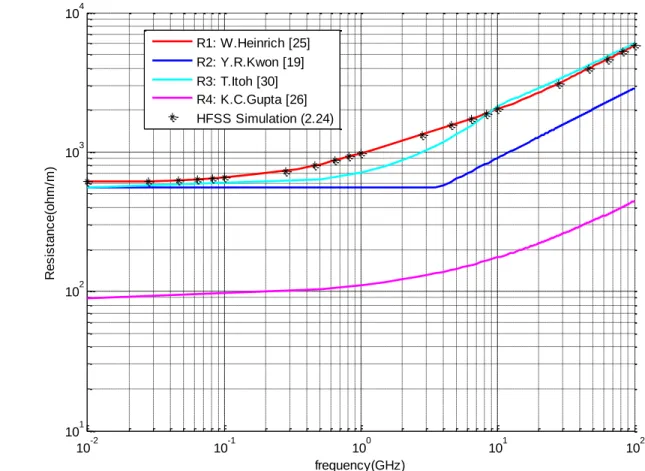
Fig 3.4: Comparison of total inductance calculations of the CPW line ... 38
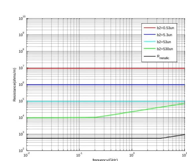
Fig 3.5 Comparison of conductor resistance calculations of the CPW line ... 40
Fig 3.6: Comparison of longitudinal substrate loss resistance ... 41
Fig 3.7: Illustration of the MIS coplanar structure and the equivalent circuit ... 42
Fig 3.8: Comparison of capacitance calculations for the insulation layer of CPW line ... 43
Fig 3.9: Comparison of conductance calculations of the semiconducting layer ... 45
Fig 3.10: MIS coplanar slow-wave structures used for the comparison of different models ... 46
Fig 3.12: Modeled results versus transverse geometrical dimensions ... 49
Fig 3.13: Calculated loss contributions versus transverse geometrical dimensions ... 50
Fig 3.14: Comparison of the modeled and simulated results ... 50
Fig 3.15: Calculated results with different semiconducting layer thickness ... 51
Fig 3.16: Modeled loss contribution results with different semiconducting layer thickness ... 52
Fig 3.17: Comparison of the modeled, simulated and reported measurement results... 53
Fig 3.18: Illustration of the thin-film MIS coplanar waveguide (MISCPW) ... 55
Fig 3.19: Effect of thickness ratio and transverse ratio. ... 56
Fig 3.20: Effect of ground distances... 57
Fig 3.21: Effect of conductivity of the semiconducting layer. ... 59
Fig 3.22: Effect of permittivity of the semiconducting layer... 59
Fig 3.23: Effect of semiconductor layer thickness. ... 60
Fig 3.24: Effect of permittivity of the insulation layer. ... 61
Fig 3.25: Effect of thickness of the insulation layer. ... 62
Fig 4.1: Resistance change of VO2 thin-film versus temperature ... 64
Fig 4.2: Microscopic structure of vanadium dioxide... 66
Fig 4.3: Two CPW lines with the same transverse dimensions but different lengths ... 68
Fig 4.4: Illustration of the VO2-loaded CPW line for semiconductor phase ... 69
Fig 4.5: CMM and PCT for CPW with two-layer substrate [60] ... 70
Fig 4.6: Illustration of the fabricated CPW line for metal phase ... 71
Fig 4.7: Measurement setup of the VO2 circuit... 73
Fig 4.8: Illustration of the fabricated reference line ... 74
Fig 4.10: Experimental results of the relative dielectric constant of the quartz substrate ... 75
Fig 4.11: Experimental results of the effective relative dielectric constant of the VO2-loaded CPW lines at varying temperatures ... 76
Fig 4.12: Experimental results for the VO2 thin-film at varying temperatures... 77
Fig 4.13: Experimental results of the effective relative dielectric constant of the VO2-loaded CPW lines at varying temperatures ... 78
Fig 4.14: Experimental results for the VO2 thin-film at varying temperatures... 79
Fig 4.15: Theoretical asymptote of the maximum measurable frequency range ... 81
Fig 4.16: Comparison of the experimental results with the literature values ... 82
Fig 4.17: The dielectric property of the mixture ... 84
Fig 4.18: Illustration of the VO2-loaded MIS coplanar delay line ... 85
Fig 4.19: Resistivity-frequency domain chart for VO2-loaded MISCPW at 22oC and 70oC.. ... 87
Fig 4.20: Electric field distribution for Line 2 at 22oC at 2.5GHz ... 88
Fig 4.21: Magnetic field distribution for Line 2 at 22oC at 2.5GHz...89
Fig 4.22: Electric field distribution for Line 2 at 70oC at 2.5GHz ... 89
Fig 4.23: Magnetic field distribution for Line 2 at 70oC at 2.5GHz...90
Fig 4.24: Attenuation and SWF of VO2-loaded MISCPW at 22oC and 70oC ... 90
Fig 4.25: Q factor of VO2-loaded MISCPW at 22oC and 70oC ... 91
Fig 4.26: Resistivity-frequency domain chart for VO2-loaded MISCPW versus temperature. ... 92
LIST OF ACRONYMS AND ABBREVIATIONS
ADS Advanced design system
CMM Conformal mapping method CPW Coplanar waveguide
HFSS High frequency structure simulator MIS Metal-insulator-semiconductor
MISCPW Metal-insulator-semiconductor coplanar waveguide MMIC Monolithic microwave integrated circuit
RF Radio frequency
S-CPW Shielded-coplanar waveguide SMT Semiconductor-metal transition SWF Slow-wave factor
SWS Slow-wave structures
PCT Partial capacitance technique P-U-L Per-unit-length
INTRODUCTION
With the increasing demand for devices that have smaller physical size, miniaturized circuit has become more and more important in modern communication systems because of its potential low cost and high portability. The Moore’s law predicts a significant miniaturization of electronic devices, which leads to the area occupied by active components that is considerably small compared to the area taken by passive monolithic components.
As the size of microwave passive components is inversely proportional to the effective dielectric constant, a substrate with sufficiently high dielectric constant can be used to miniaturize the circuit adequately at any operating frequency in order to reduce the size of distributed passive components. Unfortunately, most of relevant materials are not suitable because of their relatively low dielectric constant. The ferroelectric materials, however, are high in dielectric constant but they exhibit very high dielectric losses, which are very sensitive to temperature. Multilayered MIS (Metal-Insulator-Semiconductor) structures are shown to support slow-wave propagation by a proper selection of operating frequency, structural size and conductivity (doping level) of the semiconductor layer [1]. The support of slow-wave propagation can significantly increase the per-unit-length transverse capacitance, thus the effective permittivity of the circuit, which leads to a dramatic reduction in circuit size.
There were numerous works focusing on the analysis of MIS structures. An MIS slow-wave structure can be fabricated by depositing planar metallic patterns on the insulation layer formed or depleted on an appropriately doped semiconductor substrate. The MIS slow-wave structure can be in the form of an MIS microstrip line, MIS coplanar waveguide, MIS Schottky-contact microstrip and Schottky-contact coplanar waveguide [1]. The existence of a slow-wave mode was first predicted by Guckel [2] and verified by Hasegawa [3] in 1971. The slow-wave propagation is verified by a microstrip transmission line printed on Si-SiO2 substrates. Compared with
traditional microstrip line, this slow-wave transmission line shows a very high effective dielectric constant and also an extremely low characteristic impedance. In 1977, Hasegawa [4] proposed an MIS and Schottky coplanar slow-wave structure on GaAs substrates. The electric field is mostly confined inside the insulation layer or the depletion layer. In 1981, Seki [5] modeled a “cross-tie”
CPW line with a cascade of high/low characteristic impedance. The attenuation is reduced by one order of magnitude than that proposed in [4]. The attenuation is still higher than the corresponding CPW circuits because of its large width of strip and large gap between the strips. Recently, J. R. Long [6] has proposed a shielded passive coplanar interconnect S-CPW for silicon-based circuits. The mechanism of the proposed interconnects is the same as that in [5]. By increasing simultaneously the p-u-l inductance and the capacitance, the proposed S-CPW has a Q-factor around 22, which is over twice the Q-factor of a conventional 50 ohms coplanar waveguide from 15 to 40GHz.
The systems that exploit tunable devices potentially benefit from multi-functionality and performance enhancement. The tunability of such devices is normally realized by active electronic devices or RF-MEMS (micro-electro-mechanical systems). However, the performance of these active electronic devices are limited by non-linearity and high power consumption, while the MEMS devices have the problem of slow switching time and low reliability. Nowadays, lots of research work has been conducted on the basis of novel functional nano-materials which feature higher tunability, faster switching time and smaller size. The electrical property (resistivity, permittivity and permeability, e.g.) of those novel functional nano-materials can be controlled by external excitation (temperature variation, light illumination, applied voltage or field, etc.). Among all the attractive novel functional nano-materials are those showing phase transition like semiconductor-metal transition (SMT), vanadium dioxide (VO2) [7] has received a
special attention because of its low dimension, low transition temperature, high resistance ratio change and fast switching time [8].
It has been found that the SMT in VO2 can be induced by applying a voltage larger than the
threshold voltage across the VO2 thin films even at room temperature [9-10]. When the carrier
density is increased to a certain critical value, the SMT can be induced. This property makes the VO2 material very promising for applications in electronic circuits. Up to now, lots of
electrically-induced RF switches [9-10] are proposed, employing the ultra-fast SMT property of VO2 thin films, but all the designs are based on a resistance change model without knowing the
broadband dielectric property when designing the VO2-based RF switches. Sharp changes of the
electrical properties of VO2 on the SMT are accompanied with abrupt changes in optical
wavelengths [11]. Remarkably in 2010, Minah Seo [12] proposed a terahertz nano-screen based on VO2 phase transition. Hybridized with thin VO2 films, the ultra-broadband terahertz
nano-screen shows an extinction ratio of nearly 1×10⁴
with 4 orders of magnitude change in resistivity associated with VO2 phase transition. But the transmission at the VO2 insulating state over the
whole designed frequency range still needs to be improved. In 2008, Julien Givernaud et al [13] proposed a tunable band-stop filter design based on a fast, reversible SMT in VO2 thin films. The
operating frequency is from 11GHz to 13GHz. The filter consists of a transmission line coupled with four U-shaped resonators. The experimental results fit well with the simulation results while the insertion loss is also too high compared to the MEMS based tunable filter [14]. In 2009, Julien Givernaud et al [15] proposed a power limiting device based on the SMT in VO2 thin films.
First of all, a simple switch composed of a CPW loaded with the VO2 patterns is presented. This
power-induced switch works as a microwave "fuse" in the circuits over a broad band (from 100MHz to 40GHz), the threshold power can be tuned by external parameter like temperature or by DC voltage bias. A more complex passive power limiting device based on the former presented CPW line is proposed. The proposed power limiting device can limit the RF/MW incident power on a large band of frequency. In 2013, S. Vegesna [16] proposed a reconfigurable terahertz frequency selective structure based on VO2 phase transition. A tunable FSS polarizer
with extinction ratio of around 25 dB and a tunable bandpass FSS filter with 30 resonance frequency shifts are realized.
If the semiconductor layer in the MIS structures is substituted by the VO2 thin film whose
permittivity and conductivity can be tuned thermally, optically or electrically, we can design a new type of variable slow-wave structure. The objective of the dissertation is to design a thermally tunable MIS coplanar slow-wave structure based on the vanadium dioxide phase transition.
The thesis is organized in the following way:
Chapter 1 starts with the definition of slow-wave structure and the introduction of their different configurations. Special attentions are focused on the configurations of MIS slow-wave structures. The condition for the propagation of slow wave is explicitly given. In order to identify the three possible propagation modes inside the MIS structure, the resistivity-frequency domain chart is
used to clearly illustrate the three modes which come out from the three limiting cases of the substrate resistivity and frequency.
In chapter 2, typical configurations of the MIS coplanar slow-wave structures are first introduced, followed by the two different approaches used for the analysis of the MIS coplanar slow-wave structures. The loss mechanism is well documented and explicitly expressed in equations using the Q-TEM transmission line model. Possible ways of reducing the loss is also given. In the last section, the most important equations used for the extraction of characteristic parameters of the MIS coplanar lines from S parameters are provided.
In chapter 3, a unified equivalent circuit model is proposed for the MIS coplanar slow-wave structures. With the proposed equivalent circuit, an extensive analysis of the influence of various structural and material parameters on the characteristics of the thin-film MISCPW is investigated. This is very useful for a fast and accurate design of MISCPW with predefined slow-wave factor and minimized attenuation. This model avoids the computational complexity of the full electromagnetic solutions and calculates the characteristic parameter of these transmission lines with quite acceptable accuracy. With the proposed modeling techniques, the loss contribution from the three sources (conductor loss, transverse and longitudinal dielectric loss) can be easily calculated. Besides, we can gain much more insight into the mechanism and physics of the MIS slow-wave structures.
In chapter 4, the broadband dielectric constants of a deposited VO2 thin film versus temperature
are experimentally extracted. Based on the extracted dielectric constants, a thermally tunable MIS coplanar slow-wave structure is demonstrated based on the VO2 phase transition. The
characterization work is performed on the probe station. The measured dielectric constant is consistent with the reported results, which verifies the accuracy of the measurement results. Finally, the thermo-tunable MIS coplanar slow-wave structure based on VO2 phase transition is
presented. The designed thermo-tunable MIS coplanar slow-wave structure shows a dramatic increase in slow-wave factor when the temperature increases over transition temperature 𝑇𝑐. The attenuation is kept at a very low level, with the Q-factor is more than twice of that proposed in [4] over the whole frequency range. Obviously, the optimization of structural parameters can be performed to realize an optimum design.
The contributions of the research work presented in this dissertation are summarized in the last chapter. Even though only one design example of the thermally tunable MIS coplanar slow-wave structure is demonstrated, the modeling techniques can be extended for the rest of MIS coplanar slow-wave structures and the vanadium dioxide can be used for the design of a broad range of tunable microwave devices.
CHAPTER 1 METAL-INSULATOR-SEMICONDUCTOR (MIS)
SLOW-WAVE STRUCTURES
The guided-wave properties of a waveguide are uniquely determined by the Maxwell Equations and the boundary conditions. Uniform rectangular and circular metallic waveguides exhibit phase velocity greater than the speed of light. These kinds of waveguides are usually categorized as fast-wave structures. The slow-wave structures are transmission lines in which the guide-waves travel with phase velocity less than the reference phase velocity. The reference phase velocity is usually determined by the maximum permittivity and permeability of all the composite medium layers.
1.1 Introduction to slow-wave structures
A slow-wave structure can be obtained with artificial guided-wave structures. The basic condition for the generation of slow-wave propagation inside a waveguide is that the guided-wave structure should provide separate storage of electric and magnetic energy in space either in axial or transverse directions [1].
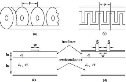
Figure 1.1: Two classes of slow-wave structure. (a) Periodic cavity-chain circular waveguide. (b) Periodic meander line. (c) MIS microstrip line. (d) MIS coplanar line.
Figure 1.1 illustrates two typical classes of slow-wave structures. In Figure 1.1(a) and Figure 1.1(b), two examples of classical periodic structures are shown. One is a cavity chain circular waveguide. The structure consists of a series of coupled resonant cavities. The smaller the center holes, the slower the phase velocity through the holes. This structure can be used to realize forward-wave travelling wave amplifiers or backward-wave oscillators. Figure 1.1(b) presents a periodic meander line. The meander line introduces a stopband in its transmission frequency response which can be regarded as low-pass behavior. Generally, the periodic slow-wave structure is formed by periodically loaded materials or periodic boundary conditions and can be analyzed by the Floquet’s Theorem. The periodic slow-wave structure is very frequency-dispersive and relatively large in size, the periodic passband and stopband are a unique feature.
Table 1.1: Basic properties of slow-wave structures [1] Transmission loss Slow-wave factor Physical size Maximum frequency Frequency dispersion Metallic periodic waveguide
Very low Low to
moderate Very large
Extremely high High Planar periodic waveguide Moderate to low Low to moderate Smaller to medium High Moderate to high Thick-film MIS lines Moderate to
high High Very small
Low (several GHz)
Relatively high
Thin-film MIS
lines Relatively low Moderate Small
Medium
(30GHz) Low
In Figure 1.1(c) and Figure 1.1(d), two examples of uniform slow-wave structures are illustrated. The Metal-Insulator-Semiconductor (MIS) structure is a typical and best-known example of the uniform slow-wave structure. Uniform MIS slow-wave structure can be in the form of microstrip
in Figure 1.1(c) or coplanar waveguide in Figure 1-1(d). The uniform MIS slow-wave structure is fabricated by depositing the planar metallic patterns on the insulation layer formed or depleted on an appropriately doped semiconductor substrate. The doped semiconductor substrate, such as N− doped silicon substrate ranges from a few micrometers (thin-film) to several hundred micrometers (thick-film). Compared to periodic structure, the frequency response is less dispersive and the size is much smaller. The reduction in phase velocity of MIS slow-wave structure is much greater than that of the periodic structure at the cost of a relatively higher transmission loss. The basic properties of the above slow-wave structures can be summarized in Table 1.1[1].
1.2 Metal-insulator-semiconductor slow-wave structures
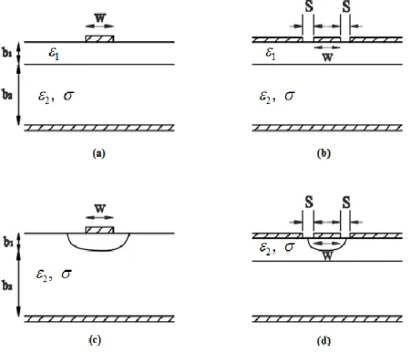
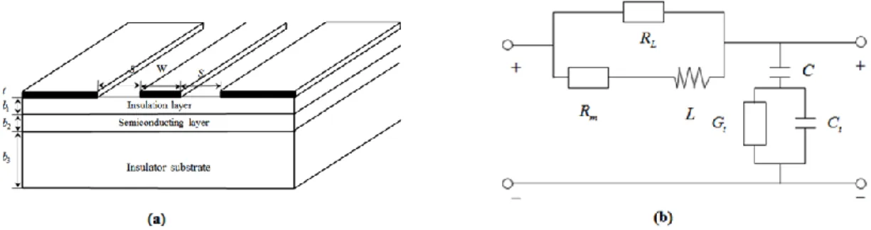
Figure 1.2: Typical configurations of MIS slow-wave structures. (a) MIS microstrip line. (b) MIS coplanar line. (c) Schottky-contact MIS microstrip line. (d) Schottky-contact MIS coplanar line.
The MIS slow-wave structure can be in the form of anMIS microstrip line (Figure 1.2(a)), MIS coplanar waveguide (Figure 1.2(b)), MIS Schottky-contact microstrip (Figure 1.2(c)) and Schottky-contact coplanar waveguide (Figure 1.2(d)).
Figure 1-2(a) presents an MIS microstrip deposited on semiconductor substrate separated by an insulator layer. The extremely thin insulation layer, silicon dioxide (SiO2) for example, ranges from sub-micrometer to around two micrometers in thickness. The line width and the gap of the MIS coplanar strip and MIS CPW, as are shown in Figure 1-3(b), range from several hundred micrometers to several micrometers. The latter is usually named micrometer-sized MIS CPW which exhibits greatly improved Q factors. The Schottky-contact microstrip and Schottky-contact coplanar waveguide, as are shown in Figure 1-3(c) and Figure 1-3(d) respectively, are special cases of MIS slow-wave structures, where the insulation layer is formed by applying the negative biasing voltage across the metallic signal line to form a depletion layer. In this way, the thickness of insulation layer can be controlled and electrically tunable SWS can be formed.
The design objective of using the MIS structure is to maximize the slow-wave factor (SWF) while minimize the attenuation when a specific characteristic impedance requirement is satisfied. For MIS slow-wave structures, attenuation constant α, propagation constant β and characteristic impedance 𝑍c are usually calculated to fully describe the performance. The characteristic impedance 𝑍c is designed for impedance matching purposes. The attenuation is often given in dB/mm or Np/mm. Sometimes, a figure of merit Q, which is defined as a comprehensive quantity to evaluate the performance of both SWF and 𝛼. The slow wave factor and the quality factor can be defined as 0 0 0 eff g p v SWF v (1.1)
1 2 g g Q (1.2)where 0 and gare free-space wavelength and guided-wave wavelength, respectively. v and 0 v p are the wave velocity in free-space and phase velocity in the waveguide. 0and are free-space propagation constant and propagation constant in the waveguide. eff is the effective permittivity
of the waveguide of a specifically designed geometry, thickness ratio of the insulation over semiconducting layer and conductivity of the semiconductor layer.
1.3 Conditions for the propagation of slow-wave in MIS structures
As mentioned in [1], the requirement for the propagation of slow-wave is the effective separation of electric and magnetic energy in space either in longitudinal or in transverse direction. The generation of slow-wave in periodic structure is normally in the longitudinal direction, whereas the generation of slow-wave in uniform structure (like MIS structure) is in the transverse direction.
The mechanism of supporting slow-wave propagation in MIS structure is that the magnetic field freely penetrates into the semiconductor layers since they are non-magnetic. The distribution of the magnetic field is almost the same as the case when no semiconductor layer exists, while the electric field is highly confined between the metallic patterns and the semiconductor layer inside the insulation layer. The effective spatial separation of electric and magnetic energy in transverse direction depends on geometry, thickness ratio and conductivity of the loaded semiconducting layer of the MIS transmission lines.
1.4 Three fundamental operating modes and resistivity-frequency chart
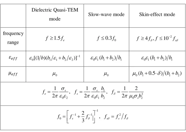
Figure 1.3: Electric field distribution of the three modes. (a) Dielectric Quasi-TEM mode. (b) Skin-effect mode. (c) Slow-wave mode [17].
It is well-known that the MIS structure can support the propagation of three modes. They are “dielectric quasi-TEM mode”, “skin-effect mode” and “slow-wave mode”. These three modes come out of three limiting cases of the substrate resistivity and frequency [3].
First of all, when the product of substrate resistivity and frequency is very large, or in its equivalent form ωε0εs ≥ σ the electric and magnetic field lines can both freely penetrate the semiconductor substrate. The fundamental propagation mode is quasi-TEM mode as shown in Figure 1-3(a). In this case, the circuit can be regarded as a two-layered dielectric consisting of the insulation layer and the semiconductor layer. The quasi-TEM analysis is valid as long as the transverse dimensions of the structure are much smaller than a half wavelength of the highest frequency. The dielectric relaxation frequency fd defines the boundary between the slow-wave mode and the dielectric quasi-TEM mode. This is the case when ωε0εs ≥ σ. The dielectric relaxation frequency fd is defined as follows
0 2 s d s f (1.3)
Secondly, when the product of substrate conductivity and frequency is very large, or in its equivalent form ωε0εs ≤ σ, the electric and magnetic field can only penetrate a small amount of thickness named skin-depth. This corresponds to the skin-effect mode as shown in Figure 1-3(b). The semiconductor layer can be regarded as a good conductor and the MIS transmission line can be analyzed as interconnects on an imperfect ground plane. In this case, the line behaves very dispersive because of the skin-effect. If we define the characteristic frequency for skin-effect as the frequency when the penetration depth is equal to the semiconductor layer thickness, we have
2 0 2 1 s f b (1.4)
Where σis the conductivity of the semiconductor layer. b2is the thickness of the semiconductor layer.
Between the above two limits there exists another form of propagation mode named “slow-wave mode” as is shown in Figure 1-3(c). In this case, the substrate conductivity is moderate and the frequency is not so high. The magnetic field can freely penetrate the semiconductor layer but the electric field is mainly concentrated inside the insulation layer just below the central signal line. Existence of the slow-wave mode was first predicted by Guckel [2] and verified by Hasegawa [3]. The characteristic frequency 𝑓0 is used to define the region for the slow-wave propagation.
Table 1.2: Properties of fundamental modes of the MIS microstrip line Dielectric Quasi-TEM
mode Slow-wave mode Skin-effect mode
frequency range f 1.5fe f 0.3f0 2 4 , 10 s f f f f 𝜀𝑒𝑓𝑓 1 0[(1 )(b b1 1 b2 2)] 0 1(b1b2) b1 0 1(b1b2) b1 𝜇𝑒𝑓𝑓 0 0 0(b10.5) (b1b2) 1 2 0 2 0 1 2 0 2 1 1 1 2 , , 2 2 2 s s e s s b f f f b b 1 1 1 2 0 2 , 3 s s s f f f f f f
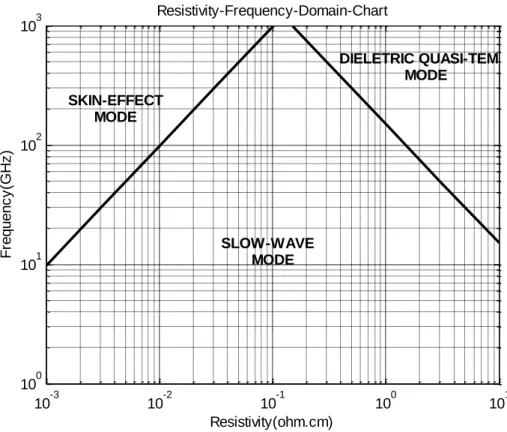
To specify the resistivity-frequency domain in which each mode propagates. The characteristic frequencies which are responsible for each of the three modes are summarized in Table 1.2 [3]. As is shown in Figure 1-2(a), if we assume an MIS microstrip structure with
14,
212,1 1 , 2 200
b m b m, with the characteristic frequencies summarized above, we can plot the above resistivity-frequency domain chart as shown in Figure 1.4, from which we can clearly identify the region for each mode.
Figure 1.4: Resistivity-frequency domain chart of an MIS microstrip line. 10-4 10-2 100 102 100 101 102 103 104 105 106 Resistivity(ohm.cm) F re q u e n c y (M H z ) Resistivity-Frequency-Domain-Chart SKIN-EFFECT MODE DIELETRIC QUASI-TEM MODE SLOW-WAVE MODE TRANSITION REGION
CHAPTER 2 FUNDAMENTALS OF MIS COPLANAR SLOW-WAVE
STRUCTURES
The coplanar waveguide (CPW) fabricated on a dielectric substrate was reported by C. P. Wen [18] in 1969. The CPW offers several advantages over the conventional microstrip line and stripline in the design of monolithic microwave integrated circuits (MMICs): First of all, the CPW is very easy to fabricate. All the signal line and the ground electrode are on the same plane, avoiding wraparound and via holes. Radiation loss and crosstalk can be greatly suppressed, but the conductor loss is high. Second, series and shunt passive and active components can be easily mounted on the circuits. Finally, the frequency dispersion in this circuit is very low and the CPW is wideband because it supports quasi-TEM modes.
2.1 Typical configuration of the MIS coplanar structure
As the coplanar MIS structures may support low-loss slow-wave propagation, they can be used to reduce the occupied circuit area and improve the quality factor. Lots of research work was focused on this topic in the last three decades [4-6].
Figure 2.1: Four typical MIS coplanar structures. (a) Thick-film MISCPW. (b) Thin-film MISCPW. (c) Inhomogeneous doped MISCPW. (d) Shielded MISCPW.
The very basic configuration of coplanar MIS structure is shown in Figure 2.1(a). The thick-film coplanar MIS slow-wave structure, which can be fabricated by depositing planar metallic patterns on the insulation layer formed or depleted on an appropriately doped semiconductor substrate. The doped semiconductor substrate, such as GaAs ranges from a few micrometers (thin-film) to several hundred micrometers (thick-film). In order to reduce the loss, Kwon [19] proposed a micro-sized coplanar MIS slow-wave structure. The frequency of slow-wave operation successfully extends to 12.4GHz and the maximum attenuation at 12.4GHz is as low as 1.5dB/mm. An equivalent circuit model was also developed which is used to predict the performance of the proposed micro-sized slow-wave structure which agrees very well with the experimental results. Of course, the thick-film slow-wave structure in Figure 2.1(a) can be also realized in Schottcky-contact form, which is a special case of coplanar MIS structure. The insulation layer is formed by applying the negative biasing voltage across the metallic signal line relative to the metal ground. In this way, an electrically tunable coplanar slow-wave structure can be formed.
Shown in Figure 2.1(b) is the thin-film coplanar slow-wave structure, in which the semiconductor layer can be realized by a thin-layer of doped silicon in the order of sub-micrometer to a few micrometers. Typical attenuation of this structure is that =0.2dB/mm and a slow-wave factor SWF=40 at 0.1GHz, but the attenuation increases to =10dB/mm and a slow-wave factor decreases to SWF=10 at 4GHz [20]. This configuration will be employed in the following chapters to design the variable slow-wave structures. The loss mechanism is largely due to the tangential electric field component along the insulator and semiconductor interface. Most of the energy is stored near the edge of the slot area, so the micro-sized coplanar slow-wave structure which minimizes the line width and the slot space can greatly reduce the loss but at the cost of reduced slow wave factor because of the reduction in the area of the transverse p-u-l capacitance calculation.
Based on the same concept, K. Wu [21] studied the in-homogeneously doped low-loss coplanar slow-wave structure as shown in Figure 2.1(c). This structure is realized by Gaussian-like inhomogeneous doped semiconductor layer which reaches the maximum just below the central signal line. Without reducing the slot distance, this structure provides a reduced effective lossy
interface by reducing the lateral doped semiconductor. The analysis is carried out using the full-wave method-of-lines numerical method and the conductor loss is included and regarded as medium in the analysis. This approach has relaxed the dimensions of a micro-sized structure by a factor of 5 and reduces the loss even further.
In Figure 2.1(d), a “cross-tie” coplanar slow-wave structure is shown. The presented cross-tie CPW includes a “cross-tie” periodic metallic ground under the conventional CPW pattern. This structure is proposed by Seki in 1981[5] and is analyzed by using the Floquet’s Theorem. The model is composed of a series of periodically alternating high impedance 𝑍𝑐,ℎ and low impedance 𝑍𝑐,𝑙, so the electric energy and magnetic energy are longitudinally and periodically stored in the high impedance region A and low impedance region B, respectively. A simultaneously increase in inductance and capacitance give rise to the propagation of slow-wave. Besides, the alternating metallic ground breaks the longitudinal current inside the semiconductor substrate, so the loss is also reduced because of a partial isolation of electric field from the lossy semiconductor layer.
2.2 Analysis of coplanar slow-wave structures
Two approaches are usually used to characterize the MIS slow-wave structure. One is an approximate and quasi-static analytical model approach. This approach avoids a great computational complexity of the full electromagnetic field solutions and calculates the characteristic parameter of these transmission lines with a quite acceptable accuracy. The approximate model neglects some unimportant electromagnetic phenomena and is based on a much simplified structure. The quasi-static model supports quasi-TEM mode propagation and the transverse dimensions are much smaller than a half wavelength. It is also assumed that the analysis frequency 𝜔 → 0.It is well-known that the MIS structure can support three modes of propagation. They are “dielectric quasi-TEM mode”, “slow-wave mode” and “skin-effect mode”. Take the MIS coplanar structure which is shown in Figure 1-2(b) as an example, one approximate quasi-TEM model is shown in Figure 2.2.
2.2.1 Approximate and quasi-static model
Figure 2.2: Approximate quasi-TEM model of the MIS coplanar structure. (a) physical configuration. (b) Equivalent circuit model.
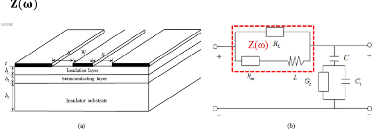
Different approaches can be used to obtain series impedance Z(𝜔) and shunt admittance Y(𝜔). Both of them can be material, geometry and frequency dependent. The key point in obtaining series impedance Z(𝜔) is to model accurately the skin-effect related conductor loss and the fringing effect. The modeling of shunt admittance Y(𝜔) involves accurate modeling of the capacitance and the conductance of the multilayer.
As indicated by Kwon [19], the quasi-TEM analysis is based on the assumption that the penetration depth of the field is much less than the skin-depth of the semiconductor. If we conservatively suppose that the penetration depth 𝑑 = 𝑠 + 𝑤/2 , then we have
2 0 1 ( 0.5 ) s f s w (2.1) This frequency 𝑓𝑠 defines the boundary between the skin-effect mode and the slow-wave mode. The dielectric relaxation frequency 𝑓𝑑 defines the boundary between the slow-wave mode and the dielectric quasi-TEM mode, we have
0 2 s d s f (2.2)
So we can conclude the frequency range for the propagation of those distinct three modes as follows:
1) Quasi-TEM mode: when the frequency range satisfies the condition of fs f fd , that is 𝜔𝜀0𝜀𝑠 ≥ 𝜎 in this case, the energy is mainly confined inside the semiconductor structure and the structure is very lossy.
2) Slow-wave mode: when the frequency range satisfies the condition of f fd, f fs. In this case, the electric energy is mainly confined inside insulation layer but the magnetic energy freely penetrate inside the semiconductor region as in the case of the conventional CPW structure with moderate substrate conductivity and frequency.
3) Skin-effect mode: when the frequency range satisfies the condition of fd f fs , that is In this case, the line is usually very dispersive and the semiconductor layer behaves like a lossy imperfect conductor.
The characteristic frequency and the lumped component values of this MIS coplanar structure can be summarized in Table 2.1.
Table 2.1: Characteristic frequency and lumped component equations [19]
𝑓𝑑 𝑓𝑠 R G L C RL MIS CPW 2 0 s s 2 0 1 1 ( ) 2 s s w 1w 2sF 0 4F 0 1 1 w K b 1 s w
Where in Table 2.1, F is the geometrical filling factor and the parameter K is the coefficient used to account for the fringing capacitance. If we assume an MIS coplanar structure as shown in Figure 2.1(a), with 14,212,b10.53m b, 2 530m,w4.2m, space s14m,with
0 s s
the characteristic frequencies summarized above, we can have the following resistivity-frequency domain chart as shown in Figure 2.3.
Figure 2.3: Resistivity-frequency domain chart of an MIS coplanar line.
2.2.2 Full-wave numerical analysis method
The second approach is the full-wave numerical analysis for the MIS structures. As the thickness ratio of the insulation layer and the semiconductor layer (or substrate layer) is quite large and the strip width is usually very small, so a 3D full-wave method such as finite element method with space-discretization is almost impossible to be used because it is very memory demanding. The method of lines [21], mode-matching method [22] and spectral-domain method [22] are usually considered to be the best choice to numerically predict the performance of the designed MIS structure. The semiconducting layer is treated as substrate with complex permittivity, and the complex propagation constant is obtained by searching a complex root of the determinant equation. 10-3 10-2 10-1 100 101 100 101 102 103 Resistivity(ohm.cm) F re q u e n c y (G H z ) Resistivity-Frequency-Domain-Chart SKIN-EFFECT MODE DIELETRIC QUASI-TEM MODE SLOW-WAVE MODE
2.3 Loss mechanism and improvement of Q factor
To identify the sources of loss in the coplanar MIS structure, the unified transmission line model is first analyzed and discussed. Theoretical equations used to evaluate the loss (conductor and dielectric loss) represented by RLGC parameters are formulated.
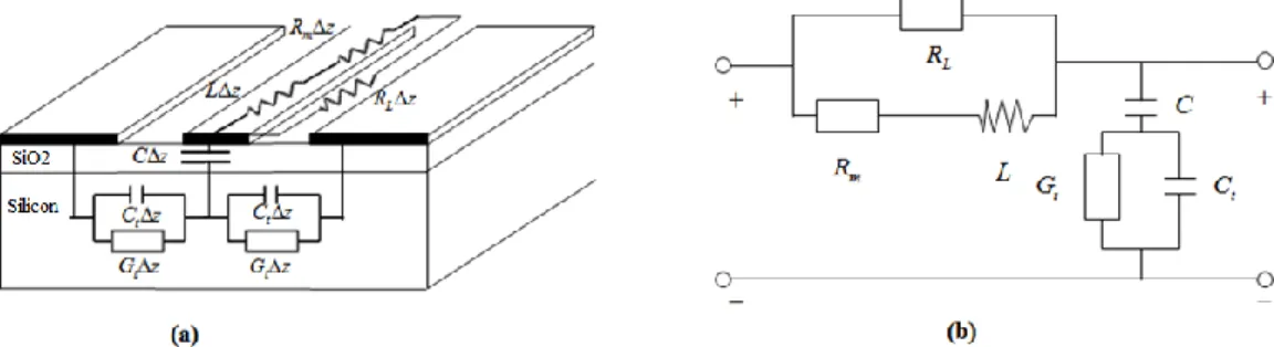
Figure 2.4: (a) Circuit model of the MIS CPW. (b) Equivalent lumped-element equivalent circuit.
( ) ( ) ( ) ( ) ( ) ( ) dV z Z I z dz dI z Y V z dz (2.3) where if we assume 𝑅𝑚 ≪ 𝜔𝐿 ≪ 𝑅𝑠𝑢𝑏 ( ) ( ) ( ) m sub sub m sub sub s R j L R j L R Z R j L R j L R Y G j C (2.4)
We can rewrite equations (2-3) in an uncoupled form
2 2 2 ( ) ( ) dV z V z dz (2.5) 2 2 2 ( ) ( ) dI z I z dz (2.6) where
( ) (1 ) 2 2 2 2 sub s sub s sub s s sub j L R ZY j C G j L R j L G G j L j LC R j C j C R (2.7)
We assume 𝜔𝐿 ≪ 𝑅𝑠𝑢𝑏 , 𝐺 ≪ 𝜔𝐶𝑠 in the above equation, and then we have
(1 ) 2 2 s sub s j L G j LC R j C (2.8) Im( ) j LCs (2.9) 2 Re( ) 2 sub s 2 s L G L LC R C (2.10)
For the coplanar MIS slow-wave structure, from equation (2.10), there are two sources of loss. One comes from the conductor loss as indicated in the first term of equation (2.10) and the other comes from the dielectric loss because of the semiconductor substrate used. The radiation loss can be ignored because of the CPW structure used.
The loss contribution of the above three types of losses is different for different kinds of MIS coplanar structure. The loss contribution versus frequency for the three types of MIS coplanar structures is summarized in Table 2.2.
To improve the quality factor which is defined as Q 2 (g)1, we can increase the SWF while at the same time minimize the attenuation constant.
To increase the SWF, the basic idea is to increase the product of inductance and capacitance per unit length. The basic MIS structure shows an increased capacitance only and the separation of the electric energy and the magnetic energy is at the transverse direction. The shielded MIS coplanar structure can be used to separate storage of electric and magnetic energy in the longitudinal direction, so both the inductance and capacitance per unit length is increased.
To reduce the attenuation, that is to reduce the effective lossy interface between the slot edges, three approaches can be used. One is the cross-tie structure which periodically isolates the electric field from the semiconductor layer; the second method is to use the micro-sized structure
which reduces the slot width; the third approach is to have a Gaussian-like inhomogeneous doping profile inside the semiconductor substrate to reduce the effective lossy interface. The design of a coplanar MIS slow-wave structure is always a compromising work between characteristic impedance, attenuation and slow-wave factor.
Table 2.2: Loss contribution for three types of MIS coplanar structures Maximum operating max f Conductor loss Transverse substrate loss Longitudinal substrate loss Thin-film MIS CPW Several GHz High to very
low Low to high low
Thick-film -meter MIS CPW Up to 30GHz High to moderate low Low to moderate Thin-film -meter MIS CPW Up to 30GHz High to
moderate low Low
2.4 Extraction of characteristic parameters of MIS coplanar structures
2.4.1 Extraction of propagation constant and characteristic impedance
For a transmission line, the basic two characteristic parameters that can be used to characterize the performance are the complex propagation constant γ and the characteristic impedance Z0. In this section, the algorithm for the extraction of the complex characteristic impedance, attenuation constant, slow-wave factor and quality factor is introduced.
Figure 2.5: S matrix definition of 2-port network.
The transmission (or ABCD) matrix is defined for a two-port circuit where the total voltage and the total current are related in matrix form as [24]
Figure 2.6: Transmission matrix definition of 2-port network.
1 2 1 2 V A B V I C D I (2.11) For a transmission line with complex propagation constant and characteristic impedance 𝑍0, the transmission matrix can be calculated as such
0 0 cosh( ) sinh( ) sinh( ) cosh( ) l Z l A B Y l l C D (2.12) From A=cosh( )l , we have
1 2
cosh ( ) ln( 1)
l A A A
(2.13) From S parameters to ABCD parameters conversion in Table 2.3, equation (2.13) is written as
1 2 2 11 21 21 1 2 l S S e K S (2.14) Where 1 2 2 2 2 2 11 21 11 2 21 (1 ) (2 ) (2 ) S S S K S (2.15) From 2 0 B Z C (2.16)
Table 2.3: S parameters to ABCD parameter conversion
ABCD S A B C D 11 22 12 21 21 (1 )(1 ) 2 S S S S S 11 22 12 21 0 21 (1 )(1 ) 2 S S S S Z S 11 22 12 21 0 21 1 (1 )(1 ) 2 S S S S Z S 11 22 12 21 21 (1 )(1 ) 2 S S S S S We have 2 2 11 21 0 2 2 11 21 (1 ) (1 ) r S S Z Z S S (2.17)
where Z is defined as the reference characteristic impedance of the measurement equipment, r which is 50 ohms in most of the cases.
As the phase is cyclically mapped from -180o to 180o, we have to convert to the real radian phase in extraction of the complex propagation constant 𝛾 and the characteristic impedance 𝑍0. The attenuation constant, slow-wave factor and quality factor can be expressed as
3 3 2 Re( ) (dB ) 8.686 Re( ) 54.55 Im( ) Im( ) (dB mm) 8.686 Re( ) 10 8.686 10 Re( ) g (2.18) 0 0 0 Im( ) SWF (2.19) 2 g Q (2.20)
2.4.2 Extraction of effective RLGC parameters
In this section, the algorithm for the extraction of p-u-l RLGC parameters of the transmission line is presented.
From Figure 2.7, the series impedance and the shunt admittance can be expressed as
Z R j L Y G j C (2.21) From the Telegraph’s equation, we know
( )( ) ZY R j L G j C (2.22) 0 Z R j L Z Y G j C (2.23) From equations (2.36) and (2.37), we have
0Re
R Z (2.24) LIm
Z0 (2.25)
0
Re G Z (2.26)
0
Im C Z (2.27)Figure 2.7: (a) Voltage and current definition for a transmission line of a unit length. (b) Lumped element equivalent for a transmission line of a unit length [23].
STRUCTURE
3.1 Introduction
Two approaches are usually used to characterize the MIS coplanar slow-wave structure. One approach is the full-wave numerical analysis. The method of lines [21], Mode-matching method [22] and spectral-domain method [22] are usually employed to numerically predict the performance of the MIS coplanar structure. But some of the above numerical methods have assumed the perfect conductor and the conductor losses are systematically ignored. The other approach is the approximate and quasi-static analytical model approach [25-35]. As the MIS slow-wave structure can be sufficiently characterized by slow-wave factor, attenuation constant and characteristic impedance, some unimportant electromagnetic phenomena can be neglected and the characteristic parameter of these transmission lines can be calculated with quite acceptable accuracy based on the much simplified structure.
There are three difficulties in accurate modeling of the MIS coplanar slow-wave structures, they are: 1. Loss including conductor loss, transverse substrate loss, and longitudinal substrate loss caused by the magnetic coupling between the conductor and the lossy semiconductor layer; 2. Total capacitance of the insulation layer because of the fringing effect; 3. the internal inductance because of the skin-effect inside the conductors. As is shown in Table 3.1, the loss contribution from the above three types of loss is different for different MIS coplanar structures. That is why different equivalent circuits were proposed and reported but few of the models can be used for both the thick-film and thin-film MIS coplanar structures. The most important factors in modeling each MIS coplanar structure are summarized in Table 3.1.
This chapter is organized as follows:
1) First, a new unified model for both thick-film and thin-film MIS coplanar slow-wave structures is proposed.
2) A comparison of the proposed model and the other techniques in modeling the p-u-l lumped element of the coplanar circuit is then made, which is very useful in checking the accurateness of the proposed equivalent circuit model.
modeling techniques in modeling both thick-film and thin-film MIS coplanar structures. The loss distribution in all of the three types of MIS coplanar structure is carefully calculated and discussed.
4) finally, an extensive analysis of the influence of conductivity of the semiconducting layer, the geometry and the thickness ratio on the performance of the MIS coplanar structure is made.
Table 3.1: Important factors in modeling different MIS coplanar structures
Conductor loss Transverse substrate loss Longitudinal substrate loss Internal inductance Fringing capacitance Thin-film MIS CPW
Thin-film micrometer MIS CPW
Thick-film micrometer MIS CPW
Figure 3.1: Approximate quasi-TEM model of the MIS coplanar structure. (a) Physical configuration. (b) Equivalent circuit model.
In this part, we will present a new unified analytical model for the MIS coplanar slow-wave structures. As shown in Figure 3.1(b), accurate modeling of the structure includes six lumped elements modeling. They are 𝐿 and 𝑅𝑚of the conductor, 𝑅𝐿 due to the magnetic coupling between the conductor and the semiconducting layer, C due to the electric energy confined inside the insulation layer, Gt and Ct due to the semiconducting layer.
3.2.1 Modeling of inductance and resistance of the conductor
As inductance 𝐿 and resistance 𝑅𝑚 are both very frequency-dependent, accurate modeling of L and 𝑅𝑚 must take into account the finite conductivity and the finite thickness of the conductors. At low frequencies, the DC calculation can be used to approximate 𝐿 and 𝑅𝑚; As frequency increases, the skin-effect occurs, when the skin-depth is less than one third of the conductor thickness t, the “Wheeler’s Incremental Inductance Rule” [61] can be used to calculate 𝐿 and 𝑅𝑚. Between these two regions, none of the above two approaches can be used. So smoothing terms are used to ensure the continuity of 𝐿 and 𝑅𝑚and the first derivative of 𝐿 and 𝑅𝑚 at transition frequencies in the intermediate region. The expressions for the calculation of 𝐿 and 𝑅𝑚 are summarized in equation (3.3) and equation (3.6) [25]:
First, the external inductance 𝐿𝑒∞ can be easily calculated as [26]
0 2 0 0 0 1 4 4 e L c F F (3.1)
' ' 0 ' , 0 0.707 2(1 ) ln ( ) 1 ( ) 1 2(1 ) ,0.707 1 ln 1 k k K k k F K k k k k (3.2)
Wherek' 1k2 , the total inductance can be calculated by equation (3.3) as the sum of the exte rnal inductance Leand internal inductance L [25] i
1 2 ( ) 2 0 0 0 0 ( ) 0 2 ( ) 2 1 1 2 0 1 1 1 1 ( ) 1 2 ( ) 2 3 4 1 2 2 2 ( ) ( ) ( ) 0 2 5 2 0 1 ( ) , ( ) 1 ( ) ( ) , ( ) 1 ( ) ( ) , 1 ( ) 4 2 z z L DC L L L L L e z L L L L e i L L L e z L L L L c g L L L L e L a L L a a L L L L L a a F F L a F , L2 (3.3) with 0 0 1 1 2 1 1 0 ' ' 2 1 ( ) ( ) 0 2 2 2 0 ( , ) 3 1 ( , ) 2 4 ( ) ( ) ( ) ( ) 2 4 DC DC g z DC c g L L z L L L L L F K k K k F F K k K k F F L F (3.4) And 0 1 2 2 0 0 0 4 4 18 , , L L L g tw tw t (3.5)