Implementation of a RTOS service for the management of the reconfiguration
Texte intégral
Figure
![Figure 2.1. The Xilinx Spartan 3E FPGA from [1]](https://thumb-eu.123doks.com/thumbv2/123doknet/5551661.132853/5.892.134.762.159.514/figure-the-xilinx-spartan-e-fpga-from.webp)

![Figure 2.3. An example of a design that uses dynamic partial reconfiguration technique[2]](https://thumb-eu.123doks.com/thumbv2/123doknet/5551661.132853/7.892.128.760.160.577/figure-example-design-uses-dynamic-partial-reconfiguration-technique.webp)
![Figure 2.4. The directory structure proposed by Xilinx company for projects that use dynamic partial reconfiguration [2]](https://thumb-eu.123doks.com/thumbv2/123doknet/5551661.132853/10.892.186.843.164.552/figure-directory-structure-proposed-xilinx-company-projects-reconfiguration.webp)
![Figure 2.5. The implementation of a bus macro [2]](https://thumb-eu.123doks.com/thumbv2/123doknet/5551661.132853/11.892.142.757.570.934/figure-implementation-bus-macro.webp)

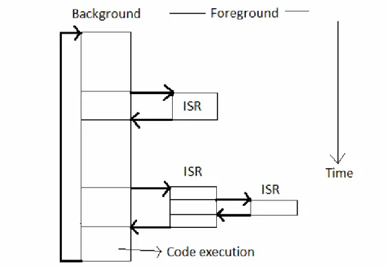
![Figure 2.8. The way a non-preemptive kernel works [18]](https://thumb-eu.123doks.com/thumbv2/123doknet/5551661.132853/15.892.153.741.656.1049/figure-way-non-preemptive-kernel-works.webp)
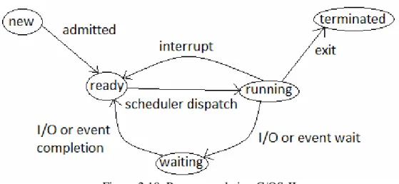
![Figure 2.9. The way a preemptive kernel works [18]](https://thumb-eu.123doks.com/thumbv2/123doknet/5551661.132853/16.892.138.758.616.1060/figure-way-preemptive-kernel-works.webp)
Documents relatifs
9.In 16---, the Pilgrim fathers , the Puritans established the
From the analysis of figure 4(a), we thus conclude that in CAP1, when the top gated surface state is charge neutral and the bulk is depleted, the bottom ungated topological
The literature reveals four major uses of the BM concept: to map specific business sectors or industries and create taxonomies; to describe the
Secondly, unlike the feature-based approach where the online classification is merely based on extracting certain features from the input SAR chip and determining where the
Jamison A., R. The Making of the New Environmental Consciousness A Comparative Study of the Environmental Movements in Sweden, Denmark and the Netherlands. Uber
57.7 and 57.17 : “The following collective rights of indigenous communes, communities, peoples, and nations are recognized and guaranteed, in accordance with the Constitution
Building on previous commitments made by our governments to our people and by the global community in favour of priority health research, including texts or instruments such as the
This situation arises over the period in which the task is active as the task organisers come to better understand what the task is seeking to achieve as a result of working to
