HAL Id: hal-00842742
https://hal.archives-ouvertes.fr/hal-00842742
Submitted on 16 Sep 2013
HAL is a multi-disciplinary open access
archive for the deposit and dissemination of
sci-entific research documents, whether they are
pub-lished or not. The documents may come from
teaching and research institutions in France or
abroad, or from public or private research centers.
L’archive ouverte pluridisciplinaire HAL, est
destinée au dépôt et à la diffusion de documents
scientifiques de niveau recherche, publiés ou non,
émanant des établissements d’enseignement et de
recherche français ou étrangers, des laboratoires
publics ou privés.
Hot Carrier Solar Cell: From Simulation to Devices
Jean Rodière, Hugo Levard, Amaury Delamarre, Arthur Le Bris, Sana Laribi,
Laurent Lombez, Jean-François Guillemoles, Jean-Philippe Perez, Philippe
Christol, Hervé Folliot, et al.
To cite this version:
Jean Rodière, Hugo Levard, Amaury Delamarre, Arthur Le Bris, Sana Laribi, et al.. Hot Carrier
Solar Cell: From Simulation to Devices. 27th European Photovoltaic Solar Energy Conference and
Exhibition (EU PVSEC 2012), Sep 2012, Frankfurt, Germany. pp.89,
�10.4229/27thEUPVSEC2012-1BO.9.4�. �hal-00842742�
HOT CARRIER SOLAR CELL : FROM SIMULATION TO DEVICES
J. Rodière1,2,3*, H. Levard1,2,3, A. Delamarre1,2,3, A. Le Bris1,2,3, S. Laribi1,2,3, L.Lombez1,2,3 & J.F. Guillemoles1,2,3 J.-P Perez4 & P. Christol4
H. Folliot5, K. Tavernier5 & O.Durand5 C. Colin6, S. Collin6 & J.-P Pelouard6
1- EDF R&D, Institut de Recherche et Développement sur l’Energie Photovoltaïque (IRDEP), 6 quai Watier, 78401
Chatou, France
2- CNRS, UMR 7174, 78401 Chatou, France 3- Chimie ParisTech, 75005 Paris, France
4- Université Montpellier 2, Institut d'Electronique du Sud (IES), CNRS, UMR 5214, 34095 Montpellier, France 5- Université Européenne de Bretagne, INSA, CNRS, FOTON, UMR 6082, F-35708 RENNES, France
6-Laboratoire de Photonique et Nanostructures (LPN-CNRS), F-91460 Marcoussis, France
ABSTRACT: Single junction III-V heterostructures based devices could overtake the Shockley-Queisser limit if thermalisation of photogenerated carriers can be strongly limited as in the hot carrier solar cell concept [1]. Previous modelling [2] and experiments [3] have shown the interest of Multiple Quantum Wells heterostructures in the antimonide system and the importance of very thin structures [3,4]. In this paper we report new data on the thermalisation rates in antimonide and phosphide heterostructures measured at ambient temperature. For the first time electrical control of hot carrier population is performed on hot carrier heterostructures devices.
Keywords: hot carrier, thermalisation, ambient temperature, heterostructures, optoelectrical measurements
1 HCSC : SLOW THE THERMALISATION
Classical PN junctions at optimum Shockley-Queisser limit already presents 30% thermalisation loss. The strategy proposed by Ross and Nozik is to effectively collect the solar spectrum by (i) reducing the absorber gap and (ii) by limiting the thermalisation process consisting in carriers-phonons inelastic interactions [3]. The proposed hot carrier solar cell (HCSC) requires high extraction regime to the terminals and a significant reduction of thermalisation rate thanks to phonon engineering.
Low temperature optical studies have pointed out MQWs as a good candidate for HCSC absorber. A 80 W/K/cm² thermalisation rate was extracted from MQWs III-V structures and has shown a 4-fold improvement compared to bulk materials [5]. Such a value would lead to a 4% efficiency increase compared to the Shockley-Queisser limit [6].
In this study, our objectives are to evidence similar measurements at room temperature under a CW excitation and attempt a first electrical control of the steady-state hot population.
2 METHOD AND EXPERIMENTS
Current-voltage I(V) and biased photoluminescence PL(V) measurements are performed simultaneously at room temperature. Samples are excited by a 975 nm cw laser at different excitation powers. The laser spot diameter is around 10 µm. The two samples are lattice matched on either a GaSb or InP substrates. Undoped GaInAsSb/GaSb or GaInAsP/InP MQWs are embedded in n and p doped high energy gap claddings to confine hot carriers. The laser excitation energy is higher than QWs barriers and lower than the claddings.
3 RESULTS AND DISCUSSIONS
3.1 I(V) measurements
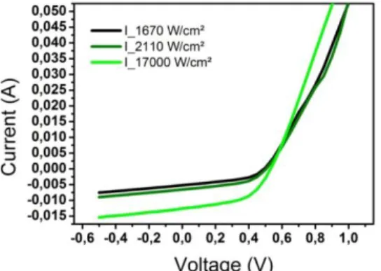
Figure 1: GaSb-sub/GaInAsSb I(V) curves at different
absorbed powers
The two samples show effective carriers extraction at reverse bias under different excitation powers (Fig. 1, Fig. 2).
In the GaSb case (Fig. 1), current injection is strongly limited above the open circuit voltage. This effect comes from a high energy gap difference between QWs barriers and the claddings (ΔEg=0.6eV). It induces an accumulation of carriers close to the claddings. Although the structure is complex, SCAPS simulation software can be used to gain insight into the electrical behavior (red curve).
In the InP based structure (Fig. 2), the barrier is much more lower (ΔEg=0.3eV), this implies a classical behaviour above the open circuit voltage even though the structure presents important shunt and series resistances.
Figure 2: InP-sub/GaInAsP I(V) curves at different
absorbed powers 3.2 T(V) measurements
As we acquire simultaneously a photoluminescence spectrum at each bias, we could extract the carrier temperature using the generalized Planck’s law [1]. For the two different samples, at a given absorbed power, we observe a temperature decrease from open circuit to short circuit (Fig. 3, Fig. 4). This effect seems to be directly correlated with the carrier density in the MQWs: extracting carriers decreases the carrier temperature.
Figure 3: GaSb-sub/GaInAsSb, T(V) curves at different absorbed powers
In the InP case (Fig. 4), we observe a temperature decrease while injecting carriers (i.e. increasing the electrical bias above the open circuit voltage). We supposed a hot carriers cooling induced by carrier’s injection from the cold reservoirs.
As we have seen in the GaSb structure I(V) curve, the injection of carriers is limited. Therefore the measured temperature does not change as we increase the electrical bias above Voc (Fig. 3).
Figure 4: InP-sub/GaInAsP, T(V) curves at different
absorbed powers.
3.3 Thermalisation rates at 300K
The thermalisation rate can be extracted from PL(V) curves. As we consider the Klemens process as the principal decomposition phonon mode, the thermalisation rate can be written as :
where Pth is the thermalised power in the absorber, The carrier temperature, T the lattice temperature, Elo the LO phonon energy and k the Boltzmann constant.
Applying the detailed balance, we get :
where Pabs is the power absorbed by the cell and Pext the electrical power extracted. As the emission power can be neglected compared to the thermalised power in III-V materials and the electrical power is equal to zero at open circuit, the thermalisation rate becomes :
From the PL(V) measurements at open circuit, thermalisation rates can be deduced from equation above and are equal to 230 and 50W/K/cm² for GaSb and InP structures respectively. Therefore, the InP heterostructure seems promising compared to previous measurements.
4 CONCLUSION
We have shown I(V) and PL(V) measurements under a continuous wave laser on MQWs samples. The experimental results show evident hot carrier population with a temperature increase higher than 150K at room temperature. The measurements were done under illumination powers of around 10000 suns. As a first attempt, we can explain the temperature changes as function of injection/extraction regimes. The low thermalisation rate found on InP based sample is promising for the HCSC concept.
5 REFERENCES
1. P. Würfel, Sol. Energy Mats. and Sol. Cells., 46, 43, 1997.
2. M.A. Green, Progress in Photovolt: Res. Appl., 9, 123, 2001.
3. R.T. Ross, A.J. Nozik, J. Appl. Phys., 53, 3813, 1982. 4. A. Le Bris et al., Journal of Photovoltaics, 2, 505-511, 2012.
5. A. Le Bris et al., Energy Environ. Sci., 5, 6225-6232, 2012.
6. A. Le Bris and J.-F. Guillemoles, Appl. Phys. Lett., 97, 113506:113508, 2010.