HAL Id: tel-00367528
https://pastel.archives-ouvertes.fr/tel-00367528
Submitted on 11 Mar 2009
HAL is a multi-disciplinary open access archive for the deposit and dissemination of sci-entific research documents, whether they are pub-lished or not. The documents may come from teaching and research institutions in France or abroad, or from public or private research centers.
L’archive ouverte pluridisciplinaire HAL, est destinée au dépôt et à la diffusion de documents scientifiques de niveau recherche, publiés ou non, émanant des établissements d’enseignement et de recherche français ou étrangers, des laboratoires publics ou privés.
Hybrid thin-film solar cells based on nano-structured
silicon and semiconducting polymer
Pierre-Jean Alet
To cite this version:
Pierre-Jean Alet. Hybrid thin-film solar cells based on nano-structured silicon and semiconducting polymer. Condensed Matter [cond-mat]. Ecole Polytechnique X, 2008. English. �tel-00367528�
Laboratoire de physique des interfaces et couches minces
Laboratoire de chimie des surfaces et interfaces
Pierre-Jean Alet
Hybrid thin-film solar cells based on
nano-structured silicon and
semiconducting polymer
Doctoral thesis in Materials Science
É c o l e
P o l y t e c h n i q u e
Thèse
présentée en vue d’obtenir le grade de docteur, spécialité
Sciences des matériaux
par
Pierre-Jean Alet
Cellules photovoltaïques en couches minces à
base de silicium nanostructuré et de polymère
semiconducteur
Thèse soutenue le 14 novembre 2008 devant le jury composé de :
Dr. Jean-Noël CHAZALVIEL École polytechnique/CNRS Président
Prof. Anna FONTCUBERTA IMORRAL EPFL, Lausanne Rapporteur
Prof. Jenny NELSON Imperial College, London Rapporteur
Dr. Serge PALACIN CEA Saclay Encadrant
Dr. Joaquim PUIGDOLLERS Universitat Politècnica de Catalunya Examinateur
Acknowledgements
I
Nthe beginning was a dream team. They came from three laboratories, they imagineda challenging multidisciplinary project, and they accepted to entrust me with it. I am much thankful to them four: Pere Roca i Cabarrocas, Muriel Firon, Anna Fontcuberta i Morral, and Serge Palacin.
Changes in the strategy and organization at CEA forced Muriel to move to com-pletely different activities. I was fortunate enough for she was still present during my first months. She largely contributed to give this thesis a good start. No matter how hectic her new position, she kept following my work throughout these three years. Merci Muriel.
Young scientists often have a nomadic life. Anna is no exception. Before I started my work, she had moved to Munich. I would have loved to work more with her, but at least her new positions gave her all the required titles and independence to be one of my rapporteurs. I could not have dreamt of someone more able for that role. I really appreciate she accepted it while moving again and starting a new team. Thank you, merci, danke, graciès Anna.
Serge Palacin welcomed me in his group in Saclay in spite of my large ignorance of chemistry. His administrative duties have constantly increased during these three years, my work remained far from his favorite research topics, yet he constantly sup-ported me, trusted me, and appropriately advised me. He is for sure a great scientist. And he is an exceptionally fair group leader. Merci Serge.
I barely spent a week in Pere’s group during my final year of master, but it was enough to make me change my mind about doing a PhD. Pere is impressive. He seems hardly human, as he knows all the tips and tricks of the reactors, as he works all the time, as he manages to cope with an overcrowded office and people queuing to see him, as he keeps track of everybody’s activity and switches topics tens of times a day. And yet he is so human. He pays attention to everyone. He grows tomatoes. He is addicted to candied ginger. And he likes frogs. Even more important for me, he is an excellent PhD advisor. He knows the difficult art of stimulating without stressing, challenging without hitting, delegating without abandoning. I have been more than lucky to work with him. Graciès Pere !
I am much thankful to Jenny Nelson for accepting to be one of my rapporteurs. It was an intimidating honor to have my work reviewed by such an inspiring and dedi-cated scientist, and it was a pleasure to answer her stimulating questions. Jean-Noël
Chazalviel accepted to chair the jury, and he did so with great commitment. He read my manuscript with an impressive attention and contributed to expel errors of any kind from this final version. I am also thankful to Joaquim Puigdollers, who taught me a lot during my short stay in Barcelona, challenged my views on many occasions, and kindly accepted to be one of my examiners.
Most of this work would not have been possible without help and collaboration from many people. I am much indebted to the organic team of CEA INES in Cham-béry, in particular Rémi de Bettignies, Stéphane Guillerez, and Séverine Bailly. They welcomed me on several occasions to perform intensive and fruitful — though some-times disappointing — runs of experiments. In addition, Stéphane traveled several times all the way to Saclay just to discuss my work. Merci beaucoup à vous trois ! Lau-rent Eude, Hee Jin Jeong, Leo Caristan, and Costel-Sorin Cojocaru, from PICM, were of great help with my first CVD experiments on the growth of silicon nanowires, and many SEM images could not have been obtained without them. Speaking of SEM, I am much thankful to Vincent Derycke, from LEM in Saclay, who trained me and al-lowed me to use theirs extensively.
In Saclay, Sylvain Foucard provided me on many occasions with the creative, re-liable experimental setups and accessories he prepared in the mechanics workshop. Some of them have been of critical importance for this work. Merci Sylvain. I have of-ten been rescued in front of reluctant reactors by the helpful technical staff of PICM, in particular Gary Rose, Jérôme Charliac, Cyril Jadaud, Olivier Godde.
I have been incredibly lucky with the qualities and friendliness of my colleagues. I shared my office, coffees, doubts, and discoveries with the outstandingly intelligent, generous, and fun dottore dottore dottore Alessandro Benedetto. Grazie mille per tutto. Guy Deniau helped me a lot in rebuilding Odile and discovering hidden trea-sures of Saclay. Pascale Jégou and Pascal Viel were strong and sensitive supporters; their attention has been priceless in times of distress or discouragement, not to men-tion their technical help. Bruno Jousselme is an enthusiastic experimenter and shares many scientific interests with me. We had lots of energizing discussions. Camille Mouton experimented my management skills. I am afraid I did not transmit her any passion for research, but she did a very serious work on P3HT and brought yet an-other touch of life and originality to LCSI. I shared with this group good science and lots of fun, lively lunches and numerous celebrations. Merci à toutes et à tous, col-lectivement et individuellement : Julienne, Brigitte, Lorraine, Vincent, Antoine, Tuan, Romain, Dimitri, Aidthia, Sébastien, Nabila, Federico, Alan, Fabrice, Achraf, Rachid, Thomas, Fabien, Corinne and Wall-E. Je vous quitte avec émotion.
In PICM, Linwei Yu deserves special acknowledgements. With his sustained en-thusiasm, his hard work, and his sparkling curiosity, he gave a great boost to the re-search on silicon nanowires and to my final year. Xièxie Linwei! I wish you arrived sooner! Jérôme Damon-Lacoste, Alexei Abramov, and Erik Johnson introduced me to the intimidating ARCAM and helped me on many occasions. I shared friendly mo-ments with them and fellow PhD students and post-docs: Roelene, Ning, Laurent, Makrina, Ingrid, Maher. . . Among them, I wish to thank Yassine Djeridane, Nans Pham and Martin Labrune, who were very helpful with experiments as well. Thanks also to
all the staff who make this lab, smoothly managed by Bernard Drévillon and Yvan Bonnassieux, a very pleasant place to work.
Some people have played a special role in my scientific education and hence to this thesis. Among them, Joaquim Nassar was a great deputy manager for research and education at ENSTA. He strongly supported me when I was considering starting a PhD, and he found the time to attend my defense. I am also grateful to committed and inspiring high school teachers who contributed to shape my intellectual life: M. Lainé, Mme Picard, M. Fischer. Merci profondément à vous.
Personal support outside work has been crucial during these years, not least to prevent me from getting (completely) crazy. I should first name my family, my mother Anne who proofread this entire document and produced a rather personal and liter-ary summliter-ary, my father Bernard and my sisters Claire, Mathilde and Lucie. Though science is quite far from their personal interests, they have been present and helpful up to my defense. It was also a blessing to be surrounded by reliable friends through-out these years. Merci François, Marion, Xavier, Benoît, Kumiko, Romain, Lucie, Xin et tous les autres. I shall also thank my fellow members of MAIOT, with whom I shared so many Wednesday lunches, RER delays, and beers at the Piano Vache. Merci à tous : François, Satchin, Alessandro, Stéphane, Stéphane, Béatrice, Éric, Clémence, Bertrand, Charlotte et al.
On a sunny summer day of 2006, a light green dress entered my life. Since then the strongest personal support by far came from Gaëlle. She proofread this document, and she cooked macaroons. Day after day, she coped with my bad mood or my over-excitement. What she brought me is far beyond the few sentences I could write here. Just thank you for what you are and what we will be.
Contents
Acknowledgements
viiContents
xIntroduction
11 Silicon/P3HT ideal hetero-junction
71.1 Introduction to the materials used in this study . . . 9
1.1.1 Semiconductors for solar cells . . . 9
1.1.2 Silicon . . . 13
1.1.3 Organic semiconductors . . . 16
1.1.4 P3HT . . . 18
1.2 Potential of the silicon/P3HT heterojunction for photovoltaics . . . 22
1.2.1 Junctions involving semiconductors . . . 23
1.2.2 Silicon/organic heterojunction in the literature . . . 25
1.2.3 Tentative band diagram. . . 27
1.3 Exploration of possible multi-layer configurations . . . 28
1.3.1 Design and fabrication of devices . . . 28
1.3.2 Effect of the structure on photovoltaic parameters . . . 29
1.4 Analysis of optimized devices . . . 30
1.4.1 Diode behavior . . . 33
1.4.2 Behavior under illumination . . . 34
Summary. . . 37
2 Real interfaces
39 2.1 Position of the problem . . . 412.2 Design and fabrication process. . . 42
2.2.1 Improvements on the design and the fabrication process . . . 42
2.2.2 Development of a new glovebox . . . 43
2.3 Interface between silicon and P3HT . . . 47
2.3.1 Technical approach: prevention and characterization of the contami-nation . . . 47
2.3.2 Analysis of the oxidation . . . 48
2.3.3 Analysis of the carbon contamination . . . 51
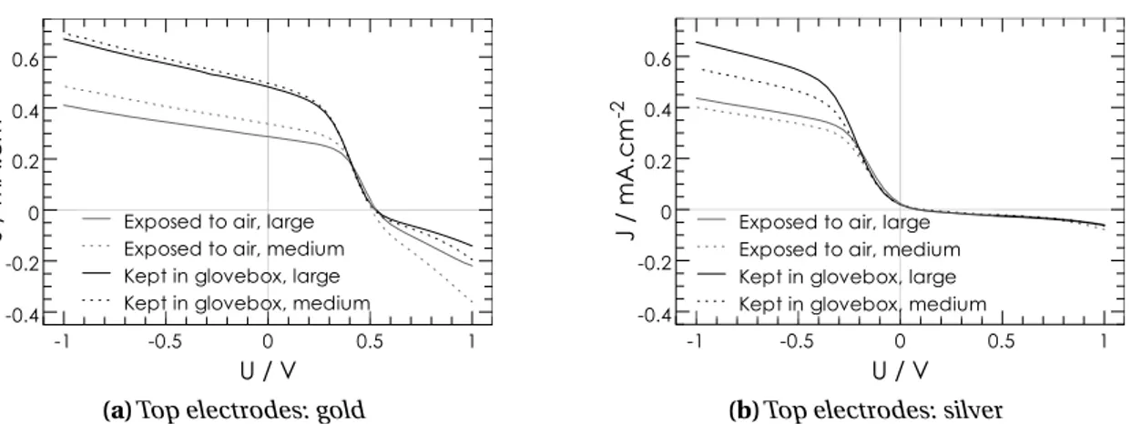
2.4 Interface between P3HT and the top electrode. . . 52
2.4.1 Defective interface between P3HT and metal electrode. . . 53
2.4.2 Improvement of the contact . . . 56
Summary. . . 60
3 TCOs as substrates for silicon nanowires
63 3.1 How can silicon nanowires be grown on a substrate?. . . 653.1.1 The “top-down” approach: etching . . . 65
3.1.2 The “bottom-up” approach: anisotropic growth. . . 66
3.1.3 Control of the orientation and the growth direction . . . 68
3.1.4 Choice and deposition of the metal catalysts. . . 70
3.2 Formation of metallic aggregates on transparent conductive oxides . . 72
3.2.1 Deposition and annealing . . . 73
3.2.2 Development and test of a characterization method. . . 73
3.2.3 Reliability of the image analysis . . . 74
3.2.4 Qualitative and quantitative evolution of the layer . . . 80
3.2.5 Summary . . . 88
3.3 CVD growth on transparent conductive oxides . . . 88
3.3.1 Experimental design . . . 88
3.3.2 SEM characterization of the deposited layers. . . 90
3.3.3 Analysis . . . 92
Summary. . . 94
4 PECVD growth of silicon nanostructures
95 4.1 Rationale for using PECVD to grow silicon nanowires . . . 974.1.1 Why are plasmas not widely used to grow nanowires? . . . 97
4.1.2 Potential advantages of plasmas for the growth of nanowires . . . 99
4.2 Nanostructured silicon on evaporated catalysts at low temperature. . . 100
4.2.1 Choice of experimental conditions . . . 100
4.2.2 Characterization of the catalytic effect . . . 102
4.2.3 Possible growth mechanism. . . 108
4.2.4 Outlook . . . 110
4.3 Hydrogen plasma on evaporated catalysts . . . 112
4.3.1 Hydrogen plasma treatments on copper and gold . . . 112
4.3.2 Hydrogen plasma treatments on indium and aluminum . . . 114
4.4 Growth of silicon nanowires with catalysts generated in-situ. . . 115
4.4.1 Evidence of the growth of silicon nanowires without external catalyst . 115 4.4.2 Crystalline structure of the wires and influence of the metals . . . 118
4.4.3 Effect of the hydrogen plasma treatment on the substrate . . . 121
4.4.4 Effects of the treatment time on the size and density of the wires . . . . 123
4.4.5 Creeping or standing nanowires?. . . 124
Summary. . . 125
5 Nano-structured devices
127 5.1 Deposition of the active layer . . . 1295.1.1 Deposition of the polymer layer . . . 129
5.1.2 Deposition of the silicon layer. . . 131
5.2 Performance of devices. . . 132
5.2.1 Devices based on silicon nanowires . . . 132
5.2.2 Devices based on silicon nano-pillars . . . 132
5.3 Discussion and outlook . . . 136
5.3.1 Performance and analysis of the devices. . . 136
5.3.2 Interface engineering . . . 139
5.3.3 Optical and electrical modeling. . . 142
Conclusion . . . 144
Conclusion
145A PECVD
149 A.1 Chemical vapor deposition. . . 151A.2 Presentation of plasma-enhanced CVD. . . 152
A.2.1 Physical characteristics of low-temperature plasmas . . . 152
A.2.2 Chemistry in the plasma . . . 154
A.2.3 RF-PECVD reactors. . . 155
B Fabrication and characterization methods for thin-film solar
cells
163 B.1 Characterization methods . . . 165B.1.1 Electrical characteristics . . . 165
B.1.2 Measurement methods . . . 168
B.2 Fabrication techniques. . . 169
B.2.1 Fabrication of multi-layer hybrid devices . . . 169
B.2.2 Evaporation under vacuum . . . 170
B.2.3 Operating procedure for ODILE . . . 172
Notations
177Bibliography
179Introduction
The ultimate answer to humanity’s energy problems rises every morning and sets every evening.
Editorial, Nature, 14thAugust 2008
There is a paradox in the world of photovoltaics. On one side, dozens, if not hun-dreds, of different materials and architectures have been investigated. They range from inorganic single-crystal single junctions to solution-processed organic tandem cells to hybrid organic/inorganic devices.1 Many of them are still active topics, either
in industry or in academic research, and we will introduce another new design in this work. On the other side, more than fifty years after the first report of cells based on crystalline silicon p-n junction,2 this structure still represents more than 90% of the
market!3
It is indeed a mature technology, which developed in parallel to the microelectron-ics industry. It has reasonable power conversion efficiencies (module efficiency above 22% in laboratory),4its stability is good (performance are commonly guaranteed over
25 years). Most importantly, its energy payback time, i.e., the required operation time for an installation to produce the amount of energy used during its production, is small (about two years) as compared to its lifetime.5So why bother developing
some-thing else? To make it short, crystalline silicon is too expensive. That is why, in spite of unique growth rates (between 30% and 40% per year for years), the contribution by photovoltaics to the global energy mix is still negligible.
The cost structure of photovoltaics is quite original. The primary source — sun-light — is really free, as it is not stored on earth, and it is almost unlimited: the sun pro-vides the earth with 10000 times the human energy consumption. So at first glance,
1Goetzberger, Hebling, and Schock, “Photovoltaic materials, history, status and outlook”, 2003
[GHS03]
2Chapin, Fuller, and Pearson, “A New Silicon p-n Junction Photocell for Converting Solar Radiation
into Electrical Power”, 1954 [CFP54]
3Platform, The Status of PV Industry, 2007 [Pla07]
4Green et al., “Short Communication Solar cell efficiency tables (Version 31)”, 2008 [Gre+08] 5Fthenakis and Alsema, “Photovoltaics Energy Payback Times, Greenhouse Gas Emissions and
Ex-ternal Costs: 2004–early 2005 Status”, 2006 [FA06]
2 Introduction the power conversion efficiency (PCE) should not be an issue. But, unlike other en-ergy sources like oil or uranium, sunlight is not concentrated. It is a flux spread all over the surface of earth. As a consequence, a given photovoltaic installation will re-ceive a finite power, proportional to its surface (of the order of 1kWm−2). So the cost per kilowatt of electricity it can produce will be determined, at a given location, by the ratio between the cost per square meter of panel and the PCE. The final cost of the produced energy, i.e., the cost per kilowatthour of electricity, will in addition depend on the lifetime of the system.
The three components of the cost (power conversion efficiency, cost per square meter, lifetime) can hardly be optimized at the same time. The problem with crys-talline silicon is its price per square meter. This is the very point thin-film photo-voltaics, in particular organic, is intended to address. Three factors are used to de-crease the costs:
• using less materials (the thickness of the active layer is between 100nm and a fewµm), and using cheap materials, as polymer semiconductors can be
ex-pected to be;
• using simple, fast, and non energy-intensive fabrication processes, like printing; • using inexpensive, flexible substrates like metal foils or polyethylene
terephta-late (PET).
In this work, we will not estimate production costs, as it is an exploratory study on a novel cell design. But we will keep in mind these three criteria, and developing simple, straightforward, low-temperature processes will be a constant guideline.
In spite of its low potential production costs, organic-based photovoltaics is not competitive yet because its power conversion efficiency is still too low, and its lifetime too short. The low efficiency comes from a major difference between organic and in-organic semiconductors. In in-organic semiconductors, light excitation does not create free charge carriers, but electron-hole pairs called excitons. As changes in electrical state and morphology are strongly correlated in organic semiconductors, these pairs cannot be easily separated: their binding energy is of the order of 0.1eV. Thermal ex-citation (27meV at room temperature) is thus too small. The difference in electron affinity at the interface between two materials is the only practical mean to dissoci-ate excitons. In that case, the electron goes (or stays) to the mdissoci-aterial with the higher electron affinity (the electron acceptor), while the hole stays (or goes) in the material with the lower electron affinity (the electron donor). What is then critical is the short lifetime of excitons. After their creation, they can only diffuse over a few nanometers before recombining. They must be separated in between to contribute to the photo-current. That gives the major criterion to make efficient organic solar cells: any point of the active organic semiconductors must be within the exciton diffusion length from an interface with a material whose electron affinity is different enough.
This requirement is hardly compatible with another one: to avoid conduction losses, there must be an electrically continuous path from the active interfaces (where
Introduction 3 free charge carriers are generated) to the electrodes (where they are collected). Two different approaches to organic-based solar cells try to balance these two require-ments.
The first approach is to make blends. In this structure, the electron acceptor and the donor are deposited at the same time, either from a single solution or by co-evaporation, and phase-separate to form nanometer-scaled domains. It has been first developed with polymer donors and fullerene derivatives as acceptors,6after fast and
efficient electron transfer between these materials have been discovered.7The size of
the domains is critical in this structure: if they are too small, the charge collection is difficult (the second requirement is not met), and if they are too large, excitons can-not be efficiently harvested at interfaces (the first requirement is can-not met). Therefore, major improvements in the PCE have been achieved by controlling this size. This has been done by changing the solvent used for the deposition8 and by thermal
anneal-ing.9 Intrinsic properties of the polymer donor, such as its bandgap and its
mobil-ity of charge carriers, also have a strong impact on the electrical performance. This was illustrated when poly(3-hexylthiophene) (P3HT) was introduced as donor.10This
polymer is still the reference for organic-based solar cells. This structure, also called
bulk heterojunction, resulted in the highest certified PCE for single-junction organic
solar cells so far: 5.4% on 0.096cm2.11 It is still limited by charge collection, as (i)
the donor and acceptor domains, respectively, are not necessarily continuous, and (ii) conduction losses bound the thickness of the active layer to about 100nm, and therefore incident light is only partially absorbed. Evolution of the morphology upon ageing can also be a drawback of this structure.
Solar cells based on blends have also been fabricated with inorganic nanocrys-tals as electron acceptors, instead of fullerene derivatives. In particular, II-VI com-pound semiconductors, such as CdSe,12have been investigated. These nanocrystals
have several potential advantages: their shape can be tuned, from spheres to rods13
to three-dimensional tetrapods;14 they can absorb sunlight and their bandgap can
be tuned to adapt the absorption spectrum of the active layer to the light. They are
6Yu et al., “Polymer Photovoltaic Cells: Enhanced Efficiencies via a Network of Internal
Donor-Acceptor Heterojunctions”, 1995 [Yu+95]
7Sariciftci et al., “Photoinduced Electron Transfer from a Conducting Polymer to
Buckminster-fullerene”, 1992 [Sar+92]
8Shaheen et al., “2.5% efficient organic plastic solar cells”, 2001 [Sha+01]
9Padinger, Rittberger, and Sariciftci, “Effects of Postproduction Treatment on Plastic Solar Cells”,
2003 [PRS03]
10Schilinsky, Waldauf, and Brabec, “Recombination and loss analysis in polythiophene based bulk
heterojunction photodetectors”, 2002 [SWB02]
11Laird et al., “Advances in Plexcore active layer technology systems for organic photovoltaics:
roof-top and accelerated lifetime analysis of high performance organic photovoltaic cells”, 2007 [Lai+07]
12Greenham, Peng, and Alivisatos, “Charge separation and transport in
conjugated-polymer/semiconductor-nanocrystal composites studied by photoluminescence quenching and photoconductivity”, 1996 [GPA96]
13Huynh, Dittmer, and Alivisatos, “Hybrid nanorod-polymer solar cells”, 2002 [HDA02]
14Sun, Marx, and Greenham, “Photovoltaic devices using blends of branched CdSe nanoparticles and
4 Introduction still limited by the same morphological issues as all-organic bulk heterojunctions and by the less efficient charge transfer at their interface with polymers than at the poly-mer/fullerene interface. So far, the highest reported PCE under simulated solar light is 2.6%.15 After efficient charge transfer between polymer semiconductors and TiO
2 has been evidenced,16metal oxide nanoparticles have also been used as acceptors in
blends.17
The second approach is to use nano-structured, porous layers filled with an organic semiconductor. It has been inspired by Dye-Sensitized Solar Cells (DSSC), where a nano-structured metal oxide is covered by a monolayer of light-absorbing molecules (the dyes) and an electrolyte.18 In this approach, light absorption and collection of
one kind of charge carriers (generally, holes) is done by a polymer semiconductor, and collection of the other kind of charge carriers (generally, electrons) is done by the metal oxide. Excitons generated in the polymer are separated at its interface with the metal oxide. As the nano-structured inorganic layer is deposited on one electrode, then covered by the polymer, the second requirement (continuous paths) is automat-ically met. The other advantage of this structure is the stability of the domain size, as it is determined by the solid inorganic layer. On the other hand, as metal oxides are wide band-gap semiconductors, they do not contribute to the photo-current. In addition, achieving the right domain size (i.e., pores with diameters about twice the diffusion length of excitons in the polymer), and a good coverage of the inorganic layer by the polymer is very challenging. That is why the PCE of devices based on this approach are still low: less than 0.3% when ZnO rods are used as the nano-structured layer.19A
comprehensive review on this topic has been published by Bouclé et al.20
A novel concept has been proposed by groups from CEA Saclay and École poly-technique21to combine the advantages of nano-structured porous layers with those
of II-VI nanocrystals used in blends. It is a design of hybrid thin film solar cells based on nano-structured silicon and polymer semiconductor,schematically shown on fig.1. In this design, silicon nanowires are used to enhance charge collection and to broaden the absorption spectrum of the active layer. If the nanowires are grown directly on the bottom electrode, continuous paths from the active interface to the electrodes will
15Sun and Greenham, “Improved efficiency of photovoltaics based on CdSe nanorods and
poly(3-hexylthiophene) nanofibers”, 2006 [SG06]
16Arango, Carter, and Brock, “Charge transfer in photovoltaics consisting of interpenetrating
net-works of conjugated polymer and TiO2 nanoparticles”, 1999 [ACB99]
17Kwong et al., “Poly(3-hexylthiophene):TiO
2 nanocomposites for solar cell applications”, 2004
[Kwo+04]
18O’Regan and Grätzel, “A low-cost, high-efficiency solar cell based on dye-sensitized colloidal TiO 2
films”, 1991 [OG91]
19Ravirajan et al., “Hybrid polymer/zinc oxide photovoltaic devices with vertically oriented ZnO
nanorods and an amphiphilic molecular interface layer”, 2006; Olson et al., “Effect of Polymer Process-ing on the Performance of Poly(3-hexylthiophene)/ZnO Nanorod Photovoltaic Devices”, 2007 [Rav+06; Ols+07]
20Bouclé, Ravirajan, and Nelson, “Hybrid polymer-metal oxide thin films for photovoltaic
applica-tions.” 2007 [BRN07]
Introduction 5 be ensured. If the distance between two wires is about twice the exciton diffusion length in the polymer semiconductor (i.e., 16nm with P3HT), the morphological re-quirement for an efficient exciton harvesting will be met.
Figure 1 –Diagram of a silicon/polymer nano-structured hybrid solar cell
In this thesis, our aim will be to determine if such devices are experimentally fea-sible, and to analyze their behavior. Indeed, to determine the relevance of this de-sign for photovoltaic applications, several questions are to be answered. Is it possible to grow silicon nanowires directly on transparent conductive oxides (TCO)? Can this growth be done with simple, low-temperature processes? Does the interface between silicon and polymer allow charge transfer and separation of excitons? Is it possible to fill the nano-structured silicon layer with the polymer? How does the nano-structure change the performance of the devices?
In the first chapter, we will investigate the hetero-junction between silicon and the polymer semiconductor we chose (P3HT). We will first present the different ac-tive materials to be used in this work. We will then discuss, on the basis of published studies, how the hetero-junction between silicon and P3HT can be described, and what its potential for photovoltaics is. Then we will experimentally investigate this hetero-junction by making and characterizing bilayer devices made of P3HT and var-ious kinds of flat silicon thin films. One structure will be selected and optimized; it will be used as our reference afterward. Part of this work has been published.22
In the second chapter, we will focus on the fabrication process and on issues raised by real interfaces. We will try to find the origin and to tackle some problems evidenced in the first chapter in the electrical behavior of the cells. In addition, we will simplify the fabrication process, and make it more reliable. We will also change the design of our samples to get more information from each experiment and prevent losses of samples because of e.g., short-circuits.
In the third chapter, we will aim at growing silicon nanowires on transparent con-ductive oxides. For that, we will present methods to grow silicon nanowires. We will
6 Introduction then select and adapt one, which is commonly used on crystalline substrates: Chem-ical Vapor Deposition (CVD) with metallic catalyst droplets. A major step will be to find a simple way to obtain nanometer-scaled metallic aggregates and to character-ize them. We chose to make these aggregates by annealing thin evaporated metallic layers. Their size and density, and their evolution mechanism, will be determined through automated analysis of SEM images. A journal article has been published on the basis of this work.23
In the fourth chapter, we will try to reduce the growth temperature of silicon nano-wires by using Plasma-Enhanced CVD (PECVD). We will first present the potential ad-vantages and drawbacks of PECVD for this. Then we will explore the effects of plasma treatments and deposition, both on metallic aggregates and on the substrates. This will allow us to define deposition processes for various nano-structured silicon thin films. In addition, we will be able to explain some surprising experimental observa-tions made in chapter 3. Three articles and one patent application have been based on this part.24
In the fifth and last chapter, we will combine all these results to make and char-acterize solar cells based on nano-structured silicon thin films. Then we will discuss our results on the basis of other published studies. We will also present some possible ways for future improvements and investigations.
23Alet et al., “Transition from thin gold layers to nano-islands on TCO for catalyzing the growth of
one-dimensional nanostructures”, 2008 [Ale+08b]
24Alet, Palacin, and Cabarrocas, “Low-temperature growth of nano-structured silicon thin films on
ITO initiated by metal catalysts”, 2009; Alet et al., “In-situ generation of indium catalyst to grow crys-talline silicon nanowires at low temperature on ITO”, 2008; Yu et al., “Synthesis, morphology and com-positional evolution of silicon nanowires directly grown on SnO2substrates”, 2008 [APC09;Ale+08a; Yu+08]
1
Silicon and P3HT: can they talk
together?
Make things as simple as possible, but not simpler. Albert Einstein
Contents
1.1 Introduction to the materials used in this study . . . 9
1.1.1 Semiconductors for solar cells . . . 9
1.1.2 Silicon. . . 13
1.1.3 Organic semiconductors . . . 16
1.1.4 P3HT. . . 18
1.2 Potential of the silicon/P3HT heterojunction for photovoltaics. . . 22
1.2.1 Junctions involving semiconductors. . . 23
1.2.2 Silicon/organic heterojunction in the literature. . . 25
1.2.3 Tentative band diagram . . . 27
1.3 Exploration of possible multi-layer configurations. . . 28
1.3.1 Design and fabrication of devices . . . 28
1.3.2 Effect of the structure on photovoltaic parameters. . . 29
1.4 Analysis of optimized devices . . . 30
1.4.1 Diode behavior . . . 33
1.4.2 Behavior under illumination . . . 34
Summary. . . 37
8 Chapter 1. Silicon/P3HT ideal hetero-junction
T
HISfirst chapter will be devoted to the study of the hetero-junction between siliconand poly(3-hexylthiophene). In particular, the relevance of such an hetero-junction for photovoltaic conversion will be investigated. We will first present the main electri-cal and optielectri-cal properties of the active materials to be used in this study. Then we will focus on the junction. On the basis of published studies, the possible nature and be-havior of the organic/silicon junction will be discussed. Possible inorganic structures will be explored and criteria for optimal devices will be given. The behavior of optimal devices will be based on optical and electrical characterizations of the materials and the devices.
The description of fabrication and characterization methods for thin-film solar cells, as given in appendixB, might be helpful at some points of this chapter.
Part of this work has been published in the European Physical Journal — Applied
Physics.1
1.1. Introduction to the materials used in this study 9
1.1 Introduction to the materials used in this study
1.1.1 Semiconductors for solar cells
Why are solar cells based on semiconductors?Solar cells are power converters: they transform energy carried by sun-light into elec-trical energy. This conversion is based on energy transfer from photons to electrons. To achieve power production, electrons must remain in an excited state long enough to reach the outer circuit. In other words, the desexcitation rate (either radiative or non-radiative) must be much lower than the excitation rate under illumination. In addition, an energetic asymmetry is required to drive these excited electrons in a par-ticular direction, thus creating a macroscopic current.
Semiconductors are defined as materials where, at 0K, the higher energy band oc-cupied by electrons is completely full and is separated from the upper band by an
energy gap, i.e., a range of energy without any possible electronic state. The same
def-inition stands for insulators; the difference lies in the width of the energy gap, Eg. A somewhat arbitrary limit is set around 5eV:2when E
g is below that value, the material is considered a semiconductor; when it is higher, the material is considered an in-sulator. This energy gap in semiconductors ensures separation between excited and ground states, which is the first requirement for an active material in solar cells. It is, in turn, one of the major constraints on the performance of the devices. Indeed, photons with energy lower than Eg will not be able to excite an electron from the ground state. On the other hand, electrons excited at energies above Eg can desexcite very fast until they reach the top edge of the energy gap. So all the energy difference between the photon energy and Eg is lost for the outer circuit. Now, sun-light is not monochro-matic, but white. Its spectrum is much like the black body spectrum at 5760K. So the conversion efficiency is limited both by the amount of photons which have en-ergies lower than Eg and by the amount of energy lost by electrons excited at ener-gies higher than Eg. Hence a compromise is necessary between these two sources of losses, which is presented on fig.1.1. The power density of sun-light at the surface of earth is plotted along with its fraction available for conversion by a crystalline silicon solar cell (Eg =1.12eV). When choosing a material for photovoltaic conversion, a ma-jor criterion is to maximize the ratio between the light and the dark gray areas. When thermodynamics is taken into account, the optimal value for Eg in a single-material solar cell is shown to be around 1.4eV, which is close to the band-gap of GaAs (1.42eV). In that case, the maximum theoretical efficiency is 33%.
The second requirement for solar cells (energetic asymmetry) is met by making rectifying junctions, i.e., by joining two materials where the chemical potential of elec-trons at equilibrium is different. Such junctions can be either metal/semiconductor junctions (Schottky junctions) or semiconductor/semiconductor junctions.
Further details on the physics of photovoltaic converters can be found in
10 Chapter 1. Silicon/P3HT ideal hetero-junction 0 0.5 1 1.5 2 2.5 3 3.5 4 0 100 200 300 400 500 600 Photon energy / eV P o w e r d e n si ty / W .m -2 .e V -1
Figure 1.1 – Power density spectrum of the sun-light at the surface of earth (light gray) and its fraction available for conversion by a crystalline silicon solar cell (dark gray)
books,3and characterization methods used in this study are described in appendixB.
Characteristic quantities of semiconductors
As mentioned before, semiconductors are primarily defined by their energy band-gap. Here we will define some of their properties that will be used throughout this docu-ment. They are schematically shown on fig.1.2.
The valence band is the band of highest energy populated by electrons at 0K. At that temperature, no free state is available in this band. The energy of its upper edge is written Ev.
No allowed states at all for electrons can be found in a range of energy above the valence band edge. The range is called the band-gap. Its width is called the band gap energy, often shortened as gap, and is written Eg.
The conduction band is separated from the valence band by the band gap. Its lower edge is written Ec. At 0K, the conduction band is completely empty. As there are no states in the band gap, an electron (from the valence band) must be provided an en-ergy larger than Eg to reach the conduction band. In general, possible energy values for electrons in a material depend on its momentum, and so do Ec and Ev. When the maximum value for Ev occurs for the same momentum value as the minimum of Ec, direct transitions from the valence band to the conduction band are possible. In that case, the material is called a direct band gap semiconductor. Otherwise, a transition
1.1. Introduction to the materials used in this study 11
Figure 1.2 – Simplified band diagram of a semiconductor evidencing its characteristic energy levels
from the valence band to the conduction band requires a change in the electron mo-mentum through interaction with a phonon4. The material is called an indirect band
gap semiconductor. This is the case of crystalline silicon. Absorption of a photon of
energy Eg to promote an electron in the conduction band is much less likely in an in-direct band gap semiconductor, where it is a three-body interaction (photon-electron-phonon), than in a direct band gap semiconductor, where it is a two-body interaction. As a consequence, the absorption coefficient of an indirect band gap semiconductor is lower than for a direct one.
The Fermi energy, noted Ef, is rather a thermodynamic quantity. Indeed, it is de-fined by the Fermi function f , which is the probability for a electronic state at an en-ergy E to be occupied when the temperature is T :
f = 1
1 + exp(E −Ef)
kBT
(1.1) The profile of the Fermi function for various temperatures is plotted on fig.1.3. The Fermi energy corresponds to the fixed point of the function family: the occupation probability is 0.5 at Ef, whatever the temperature. It can also be seen as a measure of the chemical potential of free electrons of lowest energy in a material.5 In a
semi-conductor, the actual probability of finding an electron at a given energy is given by the product of the Fermi function with the density of states, which is derived from the potential created by atoms in the material. When the semiconductor is intrinsic, i.e., there are no foreign atoms in the material, the Fermi energy lies roughly in the middle of the band gap.
The electron affinity, noted χ, is the difference between the vacuum level Evacand the lower edge of the conduction band Ec. The work function, noted φ, is the mini-mum energy to provide for an electron to be extracted from the surface of the mate-rial. In pure metals, it is well defined as the difference between the Fermi level and
4Quantum of vibration energy of the lattice
12 Chapter 1. Silicon/P3HT ideal hetero-junction 0 0.2 0.4 0.6 0.8 1 0 0.2 0.4 0.6 0.8 1 T=0K T=100K T=200K T=300K T=400K T=500K T=600K Energy / eV F e rmi fu n ct io n f
Figure 1.3 – Plots of the Fermi function for temperatures ranging from 0K to 600 K and a Fermi energyEf =0.4 eV
the vacuum level, and it can thus be measured by photo-emission spectroscopy. In semiconductors, though, it strongly depends on impurities and surface states.
Such impurities are called dopant when they are introduced on purpose in semi-conductors. When they have one extra valence electron with respect to the lattice atoms, they are generally donors, i.e., they create states in the band gap near the lower edge of the conduction band. This way, they raise the Fermi energy in the semicon-ductor. They are called n-dopant, as they increase the density n of free electrons in the material. Phosphorus is a typical n-dopant for silicon. Conversely, when they have one fewer valence electron than the lattice atoms, they are generally acceptors, i.e., they create states near the upper edge of the valence band and they lower the Fermi energy. They are called p-dopant, as they increase the density p of free holes6in the
material. Boron is a typical p-dopant in silicon. A purified semiconductor without any dopant is called intrinsic.
The electrical conductivity σ links the current flowing through a material to an external electric field. If J is the current density and E is the external electric field then, in the absence of diffusion, J = σE. The current can be carried by electrons and by holes, so the conductivity can be divided in two parts, each of which is proportional to the densities n and p of electrons and holes, respectively. This relationship is written as follows, where q is the charge of the electron:
σ = q!µnn + µpp "
(1.2) The proportionality constants µn and µp are called the electron and hole mobilities, respectively. They are defined (eq.1.3) by the critical velocity vc of these charge car-riers when they are accelerated by an external electric field E and slowed down by scattering events, which are characteristic of the material. If τ is the average time be-tween scattering events and m∗is the effective mass of the carrier, which depends on
1.1. Introduction to the materials used in this study 13 its nature and on the potential created by the lattice atoms, then:
vc!µE = qτ
m∗E (1.3)
1.1.2 Silicon
Silicon is the basis for current electronics and photovoltaics, so it is the most widely studied and described semiconductor. Here are given a few properties which will be of major importance in this study.
Silicon atoms are four-fold coordinated. Its basic pattern in solids is made of tetra-hedrons, each atom being bonded to four other ones. When a silicon atom is bonded to less than four others, some of its valence electrons are unpaired: they are called
dangling bonds. Dangling bonds are reactive sites, and they create deep electronic
states in the energy band gap. They are especially abundant at the surface of the solid, and at grain boundaries in poly-crystalline materials.
A fundamental property of silicon is its amorphous, passivating oxide, SiO2. A
na-tive oxide layer grows spontaneously on the surface of silicon when exposed to air. It
is then 2nm to 3nm thick. A denser, thicker and more uniform layer can be grown on purpose, for example by exposure to an oxygen plasma.
Crystalline silicon
Bulk crystalline silicon (c-Si) has a cubic, diamond-like crystalline structure. It is an indirect band gap semiconductor. As a consequence, its absorption coefficient in the visible range is relatively low (between 1 × 103cm−1at 1.5eV and 1 × 105cm−1at 3.1eV), which means that a thickness about 100µm is required to completely absorb
day-light. Its band gap at room temperature is 1.12eV.
In bulk crystalline silicon, charge transport is dominated by delocalized electrons in the conduction band and holes in the valence band. The electron mobility is lower or equal to µn = 1400cm2V−1s−1 and the hole mobility is lower or equal to µp = 450cm2V−1s−1. The intrinsic density of carriers at T = 300K is ni =9 × 109cm−3, so the conductivity of pure crystalline silicon is about 2.7 × 10⁻⁶Ω−1cm−1. Crystalline silicon can be n-doped with e.g., phosphorus, and p-doped with e.g., boron. Typ-ical doping levels in a p-n crystalline silicon solar cell are 1 × 1019cm−3 for n-type and and 1 × 1016cm−3 for p-type. The current record efficiency for such a solar cell is 24.7±0.5%.7
Micro-crystalline silicon (µc-Si) is made of crystallites (with typical dimensions of
a few tens of nm to 100nm) embedded in a matrix of hydrogenated amorphous sili-con (cf. section1.1.2). Its optical properties are similar to c-Si, but its transport prop-erties are dominated by grain boundaries. Indeed, they suffer both from dangling bonds8and from impurities, which tend to accumulate at grain boundaries. As a
con-sequence, the charge mobilities are much lower than in c-Si: the electron mobility
7Green et al., “Short Communication Solar cell efficiency tables (Version 31)”, 2008 [Gre+08] 8Dangling bonds can be partially passivated by hydrogen
14 Chapter 1. Silicon/P3HT ideal hetero-junction
µe is between 10cm2V−1s−1 and 30cm2V−1s−1, and the hole mobility µp is between 0.5cm2V−1s−1and 1cm2V−1s−1in intrinsic µc-Si.9 It is usually incorporated in devices
as a thin film (a fewµm in thickness). In this work, micro-crystalline silicon is
de-posited by Plasma-Enhanced Chemical Vapor Deposition (PECVD, see appendixA). Amorphous silicon
Both the structure and the properties of amorphous silicon are very different from crystalline silicon. It is still based on tetrahedron-bonded silicon atoms, but there are large variations (up to ±10◦) of bonding angles with respect to what they are in c-Si (109◦28′). As a consequence, whereas in c-Si rings10 have always six atoms, in
amorphous silicon they can have down to four and up to eight atoms (six is still the most probable number). This also leads to an increase in the amount of dangling bonds, even in the bulk of the material. Bonding distortions induce a modification of the density of states at the edge of the valence and conduction bands: instead of a parabolic decrease to zero, there are smooth transitions, which are called band tails, between the bands of spatially delocalized states (conduction and valence bands) and the band gap. In addition, dangling bonds create a continuum of localized states be-tween the conduction and the valence bands. Consequently, there is no real band gap,
i.e., an energy range where the density of states would be zero. The density of states
is still several orders of magnitude lower between the conduction and valence bands than in these bands. This region is called the mobility band gap because the mobility of charge carriers in spatially localized states is much lower than in delocalized states. The typical shape of the density of states in amorphous silicon is shown on fig.1.4.
Pure amorphous silicon is quite useless for electronic applications. In particular, the Fermi level is mainly defined by the dangling bonds. Since their number is very large, it can hardly be modified by doping. This problem has been solved by alloying amorphous silicon with hydrogen.11Hydrogen atoms are small enough to insert in the
lattice, where they bond to silicon atoms bearing unpaired electrons. Thus they pas-sivate dangling bonds and reduce the density of states in the mobility band gap by up to four orders of magnitude. The resulting material is called hydrogenated amorphous
silicon (in short, a-Si:H). Thanks to the passivation of dangling bonds by hydrogen,
a-Si:H can be doped with, e.g., boron or phosphorus. Hydrogenated amorphous sili-con can be deposited from silane (SiH4) by PECVD (see appendixA). In a-Si:H, dan-gling bonds are passivated not only in the bulk but also at the surface. As a conse-quence, it is more stable in air than c-Si or µc-Si.
The optical properties of amorphous silicon derive from its particular distribution of density of states. In particular, its absorption spectrum has a quadratic part, which results from band-to-band absorption, and an exponential part, which results from
9Damon-Lacoste, “Vers une ingénierie de bandes des cellules solaires à hétérojonctions a-Si:H/c-Si.
Rôle prépondérant de l’hydrogène.” 2007 [DL07]
10Shortest circuit through individual bonds from an atom back to it
11Spear and Le Comber, “Substitutional doping of amorphous silicon”, 1975; Street, “Doping and the
1.1. Introduction to the materials used in this study 15 -1 -0.5 0 0.5 1 1x10¹⁷ 1x10¹⁸ 1x10¹⁹ 1x10²⁰ Energy / eV D e n si ty o f st a te s Localized states (dangling bonds) Exponential band tails Quadratic band edges Mobility band-gap Ev E c
Figure 1.4 – Typical shape of the density of states in amorphous silicon (continuous lines). The dashed lines represent the case of a crystalline semiconductor with similar band gap (quadratic band edges)
tail-to-tail absorption. In the quadratic region, the absorption coefficient α is given by: α = Cste × (E − ETauc)2. The characteristic energy ETaucis called the Tauc gap and is generally considered the value of the optical band gap. Depending on the mod-els, the difference between mobility and absorption band gaps is a constant, which is of the order of 0.1eV. Amorphous materials have necessarily direct optical band gaps.12 As a result, absorption is much stronger in amorphous silicon than in
crys-talline silicon (about one order of magnitude higher in the visible range). In the case of a-Si:H, the Tauc gap depends on the hydrogen content and ranges between 1.5eV and 1.9eV.13Hydrogenated silicon layers used in this study have typical band gaps of
1.7eV to 1.8eV.
Conduction can be split in three mechanisms:
1. Band conduction: as in crystalline semi-conductors, charge can be carried by electrons and holes in delocalized band states (in the conduction band and the valence band, respectively).
2. Hopping between tail states.
12The wavenumber k of the electrons cannot describe their motion in disordered materials because
of their random scattering. As a result, no dispersion relation E = f (k) exists, and indirect transitions are undefined.
13Heuvel, Geerts, and Metselaar, “The relation between the optical properties and the hydrogen
16 Chapter 1. Silicon/P3HT ideal hetero-junction 3. Tunneling between deep localized states.
As could be expected from a disordered material, the mobilities of charge carriers are low as compared to crystalline silicon: it is about 1cm2V−1s−1 for electrons and 1 × 10⁻²cm2V−1s−1for holes.
1.1.3 Organic semiconductors
Organic molecules are based on carbon backbones, hydrogen, and functional groups based on other atoms (mainly oxygen, nitrogen, and sulfur). They are called this way because life on earth is based on such molecules. They are also the basis for many common materials such as plastics, which are insulators.
Organic semiconductors are conjugated molecules, i.e., their backbone is made of alternate single (σ) and double (σ+π) bonds between carbon atoms. Each atom con-tribute on average to one single and one double bond with its neighbors, so there are two equivalent configurations of the molecule. Resonance between those two states induce delocalization of the π bonds. Those two states for trans-polyacetylene14are
shown on fig.1.5. Defects are created when this alternating pattern of single and dou-ble bonds is broken and one carbon atom is single bonded to both its neighbors. This carbon atom bears an unpaired valence electron so it is highly reactive. This unpaired electron can be removed through an oxidation reaction, which leaves a positively charged carbon atom (a carbocation) in the backbone of the molecule. Alternatively, a reduction reaction can bring an additional electron to stabilize the unpaired electron. This reaction leaves a negatively charge carbon atom (a carbanion) in the molecule. Both kinds of charged defects can move along the backbone and carry current. That is how organic semiconductors can be made conductive. From an electrical point of view, carbocations behave as holes do in inorganic materials and carbanions behave as electrons, so they are commonly called this way for convenience.
As the length of single and double bonds is different,15there is a coupling between
electronic states and atomic positions. Creation of free charge carriers, as described above, induces a modification of the bonding pattern. As a consequence, it creates a distortion of the molecule, which coherence distance in polymers is typically 2nm. This coupling is a fundamental characteristic of organic semiconductors. In partic-ular, excitons, i.e., carbocation/carbanion pairs, are bonded together by electrostatic interaction, and by the force which tends to minimize the distortion of the molecule by keeping the defect localized. This way, their binding energy ranges typically be-tween 0.1eV and 1eV, whereas the binding energy of electron-holes pairs in inorganic semiconductors is below the thermal energy at room temperature (25meV). The most developed application of organic semiconductors to-date, OLED16, takes advantage
14Metallic conductivity in this polymer, when doped with iodine, was discovered in 1974 by Alan
Heeger, Alan MacDiarmid and Hideki Shirakawa, who were therefore granted the Nobel prize for chem-istry in 2000
15It is 0.145nm and 0.135nm, respectively, in a linear carbon chain 16Organic Light-Emitting Diodes
1.1. Introduction to the materials used in this study 17 H C C H H C C H H C C H H C C H H C C H H C C H * * H C C H H C C H H C C H H C C H H C C H H C C H * *
Figure 1.5 – Diagram of a part of a fully conjugated polymer (polyacetylene) showing its two possible states
of this spatial confinement of electron-holes pairs, as this maximizes their probabil-ity to recombine radiatively. Unfortunately, for solar cells, recombination of electrons with holes is a major source of losses and easy separation of excitons is sought.
Organic semiconductors have some sort of a band structure, which comes from the hybridization of atomic orbitals of their constituent atoms into molecular orbitals. In particular, an energy gap separates the filled, bonding (π) states from the empty, anti-bonding (π∗) states. The highest π state is called HOMO (Highest Occupied Molec-ular Orbital) and the lowest π∗ state is called LUMO (Lower Unoccupied Molecular Orbital). An analogy is usually drawn between, first, the HOMO level and the valence band edge Ev and, second, the LUMO level and the conduction band edge Ec. This analogy is convenient but one must keep in mind that, as stated in their names, the HOMO and LUMO levels are defined for molecules (including polymers), not for ma-terials. This has two major consequences. First, as the number of atoms in a molecule is limited, there is no continuum of states in the π and π∗ bands. Second, optical properties, which derive from the band structure, are modified by inter-molecular in-teractions when one goes from isolated molecules (e.g., in solution) to thin films.
The power of organic synthesis allows to create a huge range of different molecules. This is an advantage, as their properties (in particular, optical absorption) can be tai-lored for specific applications. This is also a drawback, as their number and their diversity make it difficult to draw a consistent picture of their behavior, and to check their relevance for application in real devices. Indeed, optimal device structure de-pends on the material, and it is difficult to predict potential performance of a material from the results on unoptimized devices.
Organic molecules are split in “small” molecules (i.e., without repetition of a pat-tern) and polymers, made of a large (>100) number of similar units bonded together. Small molecules are generally deposited by evaporation under vacuum, whereas poly-mers are processed in solution at atmospheric pressure. A complete discussion of the structure and properties of organic semiconductors is far beyond the scope of this
18 Chapter 1. Silicon/P3HT ideal hetero-junction document. For further details, numerous reviews and books are available.17 P3HT
was chosen as the organic semiconductor for this study. Its main properties and rea-sons for this choice are presented in the next section.
1.1.4 P3HT
P3HT stands for poly(3-hexylthiophene). It is a conjugated polymer based on thio-phene rings, i.e., conjugated ring with four carbon atoms and one sulfur. Oligothio-phenes18and polythiophenes have been widely studied for electronic (thin-film
tran-sistors) and opto-electronic (solar cells) applications. Some of the most efficient all-organic solar cells to date are based on P3HT blended with fullerene derivatives, with power conversion efficiencies about 4.4% and short-circuit current densities higher than 10mAcm−2.19 In addition, both accelerated and real, outdoor ageing
measure-ments have shown that these devices are among the most stable organic ones.20
Organization and electrical properties of thin films
Alkyl side-chains, among which hexyl chains, have been added to polythiophene to make it soluble in organic solvents. One-dimensional transport and optical properties of isolated polymer chains essentially depend on the thiophene backbone. In particu-lar, the optical band gap decreases when the number of thiophene units increases. But the materials properties, such as the charge carrier mobility in thin-film transistors, or the absorption spectrum of deposited layers, have been shown to be highly dependent on the organization of the polymer chains with respect to each other and to the sub-strate. Indeed, two-dimensional transport requires charge transfers between different polymer chains. As charges are mainly carried in π orbitals, overlap between such or-bitals of neighbor chains is highly desirable. This can be achieved when conjugated (thiophene) rings of different chains are close and parallel to each other.21Such an
or-ganization is called “π-stacking”. Side chains play a major role in this oror-ganization. In particular, they can be bonded to the thiophene ring at two different places (on each of the carbon atom not bonded to neighbor rings). The regularity of this position has a dramatic impact on the properties of polythiophenes: whereas regio-random22
17Coropceanu et al., “Charge Transport in Organic Semiconductors”, 2007; Attias, “Polymères
con-jugués et polymères conducteurs électroniques”, 2002 [Cor+07;Att02]
18Ackermann, “Study of the growth and the electronic properties of thin films based on
oligothio-phenes : Influence of the molecule structure”, 2002 [Ack02]
19Kim et al., “A strong regioregularity effect in self-organizing conjugated polymer films and
high-efficiency polythiophene:fullerene solar cells”, 2006 [Kim+06]
20De Bettignies et al., “Accelerated lifetime measurements of P3HT:PCBM solar cells”, 2006; Hauch
et al., “Flexible organic P3HT:PCBM bulk-heterojunction modules with more than 1 year outdoor life-time”, 2008 [DB+06;Hau+08]
21Sirringhaus et al., “Two-dimensional charge transport in self-organized, high-mobility conjugated
polymers”, 1999 [Sir+99]
1.1. Introduction to the materials used in this study 19 P3HT makes amorphous films, regio-regular23P3HT shows some crystallinity.24Even
the band gap is modified, from 2.1eV in regio-random P3HT to 1.7eV in regio-regular P3HT. That is why the latter is used in this study, as in most research to date. For simplicity, we will still refer to it simply as P3HT. Its formula is sketched on fig.1.6. Synthesizing polymers with high regio-regularity is a difficult task, which makes them expensive (around 300€ per gram in research quantities). It is based on Zn medi-ators.25 Commercial polymers have been used throughout this study. Most results
have been obtained with only two batches, one from Sigma-Aldrich26 and one from
Rieke Metals. S S S C6H13 C6H13 C6H13 * *
Figure 1.6 – Formula of regio-regular, head-to-tail poly(3-hexylthiophene-2,5-diyl) (in short, P3HT), as used in this work
Many other factors have significant impact on the properties of P3HT, especially on its charge carriers mobility: deposition technique,27 substrate, boiling point of
the solvent,28 thermal treatments,29 molecular weight (proportional to the number
of thiophene units per polymer chain).30 In general, long chains and well crystallized
layers give the best results. That is why using high boiling point solvents (which evap-orate slowly), and slowly cooling down31annealed layers enhance the performance, as
polymer chains have more time to organize. Highest reported mobilities of undoped P3HT is about 0.1cm2V−1s−1 for holes and 1 × 10⁻⁴cm2V−1s−1 for electrons. They
23where the positions of alkyl side-chains follow a periodic pattern
24Chen, Wu, and Rieke, “Regiocontrolled Synthesis of Poly(3-Alkylthiophenes) Mediated by Rieke
Zinc - Their Characterization and Solid-State Properties”, 1995 [CWR95]
25Chen and Rieke, “The first regioregular head-to-tail poly(3-hexylthiophene-2,5-diyl) and a
regiorandom isopolymer: nickel versus palladium catalysis of 2(5)-bromo-5(2)-(bromozincio)-3-hexylthiophene polymerization”, 1992 [CR92]
26Batch number: 10118TB, molecular weight: 4115gmol−1, received September 2004, open March,
10th, 2005
27Surin et al., “Relationship between the microscopic morphology and the charge transport
proper-ties in poly(3-hexylthiophene) field-effect transistors”, 2006 [Sur+06]
28Chang et al., “Enhanced Mobility of poly(3-hexylthiophene) transistors by spin-coating from
high-boiling-point solvents”, 2004 [Cha+04]
29Cho et al., “Thermal annealing-induced enhancement of the field-effect mobility of regioregular
poly(3-hexylthiophene) films”, 2006 [Cho+06]
30Verilhac et al., “Effect of macromolecular parameters and processing conditions on
supramolecu-lar organisation, morphology and electrical transport properties in thin layers of regioregusupramolecu-lar poly(3-hexylthiophene)”, 2006 [Ver+06]
20 Chapter 1. Silicon/P3HT ideal hetero-junction have been obtained for large molecular weight (> 30kgmol−1), highly regio-regular (>98%) polymers dissolved in trichlorobenzene (boiling point: 213◦C). Whereas the hole mobility is very similar to what it is in a-Si:H, the electron mobility is four orders of magnitude lower.
Deposition
Most polymer depositions in this work have been done by spin-coating. The princi-ple of this method is schematized on fig.1.7. Aspiration by a small pump maintain the substrate on its holder without mechanical constraint. After a small amount of polymer in solution is deposited on the substrate, high speed rotation (typically 1000 to 3000 revolutions per minute) first spreads evenly the liquid on the substrate, then helps uniform evaporation of the solvent. Such a method is very convenient for fast deposition of thin (from 10nm to few hundreds of nanometers), uniform layers on small substrates (typically, few square centimeters). In the case of P3HT, π-stacking of the polymer chains occurs during evaporation of the solvent. It induces a change in color, from orange to bronze. In this work, chlorobenzene and ortho-dichlorobenzene were generally used as solvents. The standard procedure for spin-coating was: 40s at 1500rpm with 4s ramp-up for spreading the solution, followed by 20s at 2000rpm with 4s ramp-up for evaporating the solvent.
Figure 1.7 – Principle of polymer deposition by spin-coating
The thickness of spin-coated layers can be controlled by several parameters: sol-vent (viscosity and boiling point), concentration of the polymer solution and rotation speed. The influence of these parameters is shown on fig.1.8. In our experiments, the thickness showed a polynomial dependence on the concentration, with large differ-ences when the solvent is changed (fig.1.8a). On the other hand, it decreases expo-nentially when the rotation speed during the first step increases (fig.1.8b).
Optical properties and energy levels
Position of the HOMO and LUMO levels in P3HT is a debated question and seems to depend on many processing parameters. As shown on tab.1.1, reported values for the
1.1. Introduction to the materials used in this study 21 10 15 20 25 0 3 0 0 6 0 0 Chloroforme Chlorobenzene Toluene th ic k n e ss / n m concentration / g.L-1
(a) Influence of the solvent and the solution
concentration 0 500 1000 1500 2000 40 60 80 Rotation speed / rpm T h ic k n e ss / n m
(b) Influence of the rotation speed during the
first step
Figure 1.8 – Influence of process parameters on the thickness of spin-coated P3HT layers
HOMO level vary over a range of 0.5eV.32
Level/eV Method Reference
-4.7 photo-electron spectroscopy
measure-ments in air
[Tak+05] -4.7 to -5.1 electrical measurements under vacuum on
Au/P3HT/Au sandwich devices
[Chi+03]
-4.77 electrosprayed P3HT on ITO,
measure-ment by Ultraviolet Photo-electron Spec-troscopy under Ultra-High Vacuum
[Yi+06]
-4.9 literature survey [Rav+06]
-5.2 derived from electrical measurement
under vacuum after 6h storage at 1 × 10⁻⁶mbar
[Tha+07]
Table 1.1 –Reported positions of P3HT HOMO with respect to the vacuum level As we will see later, such a variation is a major concern for us. Indeed, P3HT will be contacted with gold, whose work function is 4.8eV.33 If the HOMO level of P3HT
is lower than −4.8eV, the contact with gold will be non-ohmic. Cyclic voltammetry
32Takahashi et al., “Porphyrin dye-sensitization of polythiophene in a conjugated polymer/TiOp-n
hetero-junction solar cells”, 2005; Chirvase et al., “Electrical and optical design and characterisation of regioregular poly(3-hexylthiophene-2,5diyl)/fullerene-based heterojunction polymer solar cells”, 2003; Yi et al., “Characterization of indium tin oxide surfaces and interfaces using low intensity x-ray photoemission spectroscopy”, 2006; Ravirajan et al., “Hybrid polymer/zinc oxide photovoltaic devices with vertically oriented ZnO nanorods and an amphiphilic molecular interface layer”, 2006; Thakur et al., “Charge injection mechanism across the Au-poly(3-hexylthiophene-2,5-diyl) interface”, 2007 [Tak+05;Chi+03;Yi+06;Rav+06;Tha+07]