HAL Id: hal-02999566
https://hal.archives-ouvertes.fr/hal-02999566
Submitted on 10 Nov 2020HAL is a multi-disciplinary open access archive for the deposit and dissemination of sci-entific research documents, whether they are pub-lished or not. The documents may come from teaching and research institutions in France or abroad, or from public or private research centers.
L’archive ouverte pluridisciplinaire HAL, est destinée au dépôt et à la diffusion de documents scientifiques de niveau recherche, publiés ou non, émanant des établissements d’enseignement et de recherche français ou étrangers, des laboratoires publics ou privés.
Room temperature gas nanosensors based on individual
and multiple networked Au-modified ZnO nanowires
Oleg Lupan, Vasile Postica, Thierry Pauporté, Bruno Viana, Maik-Ivo Terasa,
Rainer Adelung
To cite this version:
Oleg Lupan, Vasile Postica, Thierry Pauporté, Bruno Viana, Maik-Ivo Terasa, et al.. Room tem-perature gas nanosensors based on individual and multiple networked Au-modified ZnO nanowires. Sensors and Actuators B: Chemical, Elsevier, 2019, 299, �10.1016/j.snb.2019.126977�. �hal-02999566�
1
Please cite this article as:
Oleg Lupan,1,2,3,* Vasile Postica,2 Thierry Pauporté,3 Bruno Viana,3 Maik-Ivo Terasa,1 Rainer
Adelung,1
Room temperature gas nanosensors based on individual and multiple
networked Au-modified ZnO nanowires.
Sensors & Actuators: B. Chemical 299 (2019) 126977 DOI: 10.1016/j.snb.2019.126977
1 Functional Nanomaterials, Faculty of Engineering, Institute for Materials Science, Kiel University,
Kaiserstr. 2, D-24143, Kiel, Germany
2 Center for Nanotechnology and Nanosensors, Department of Microelectronics and Biomedical
Engineering, Technical University of Moldova, 168 Stefan cel Mare Av., MD-2004 Chisinau, Republic of Moldova
3 PSL Université, Institut de Recherche de Chimie Paris, ChimieParisTech, UMR CNRS 8247, 11 rue
Pierre et Marie Curie 75231 Paris cedex 05, France
*Corresponding authors
Prof. Dr. Eng. Lupan, Prof. Dr. Adelung E-mails: ollu@tf.uni-kiel.de ra@tf.uni-kiel.de
Institute for Materials Science, Kiel University, Germany
Prof. Dr. Thierry Pauporté E-mail: thierry.pauporte@chimieparistech.psl.eu
PSL Université, ChimieParisTech, France
2
Abstract
In this work, we investigated performances of individual and multiple networked Au nanoparticles (NPs)-functionalized ZnO nanowires (NWs) integrated into nanosensor devices using dual beam focused ion beam/scanning electron microscopy (FIB/SEM) and tested them as gas sensors at room temperature. Such important parameters as diameter and relative humidity (RH) on the gas sensing properties were investigated in detail. The presented results demonstrate
that thin Au/ZnO NWs (radius of 60 nm) have a gas response of Igas/Iair ~ 7.5 to 100 ppm of H2
gas which is higher compared to Igas/Iair ~ 1.2 for NWs with a radius of 140 nm. They have a low
dependence of electrical parameters on water vapors presence in environment, which is very important for practical and real time applications in ambient atmosphere. Also, the devices based
on multiple networked Au/ZnO NWs demonstrated a higher gas response of Igas/Iair ~ 40 and a
lower theoretical detection limit below 1 ppm compared to devices based on an individual NW due to the presence of multiple potential barriers between the NWs. The corresponding gas sensing mechanisms are tentatively proposed. The proposed concept and models of nanosensors are essential for further understanding the role of noble metal nanoclusters on semiconducting oxide nanowires and contribute for a design of new room-temperature gas sensors.
1. Introduction
The demand for new room-temperature nanosensors has come from different fields and requirements, such as rapid detection of explosive and hazardous gases, compounds and various risky nanomaterials. Due to their high surface-to-volume ratio and crystallinity, the one-dimensional (1-D) semiconducting oxide nanostructures, such as nanowires, nanobelts, nanofibers and nanotubes, have attracted great interest toward their integration in high performance sensing devices and nanodevices [1-8]. A lot of attention has been paid especially on devices based on
3
individual 1-D nanostructures due to their unique opportunity to develop high sensitivity at room temperature, being one of the best candidates for realizing ultrasensitive gas sensors with ultra-low power consumption [2]. For example, Zhang et al. reported on the fabrication of a gas sensor
based on an individual In2O3 NW able to detect NO2 down to the ppb level at room temperature
[9]. Another huge advantage of individual 1-D nanostructures arises from their diameter comparable with the Debye length, which gives the possibility for an efficient modulation of the conduction channel under adsorption/desorption of gas molecules [3, 10, 11]. Therefore, several studies demonstrated that in the case of individual 1-D nanostructures the size is the key factor which determines the performances of the devices [7, 10, 12-17]. Yang et al. demonstrated that
smaller palladium NWs show accelerated response and recovery rates to H2 gas [18]. Tonezzer
and Hieu characterized SnO2 NWs with different diameter sizes as NO2 sensors and observed that
thinner NWs show higher gas sensing performances, i.e. a higher gas response, a smaller detection limit and faster response and recovery times [19].
Previous studies demonstrated that individual ZnO and Ag- or Cd-doped ZnO NWs, integrated into nanosensors using the same procedure, possess a good selectivity to hydrogen gas at room temperature compared to other reducing gases [14, 20-22]. The highly efficient approach to further increase the gas sensing properties and to improve the specificity of individual 1-D nanostructures is surface functionalization with noble metal nanoparticles [3, 15, 23]. In this case, nanoscale Schottky barriers are formed at the interface of metal oxide nanostructures and noble metal NPs, which greatly improve the modulation of the conduction channel under adsorption/desorption of oxygen species, i.e. lead to a higher gas response [3, 15, 23]. This gas sensing mechanism is widely attributed to electronic sensitization [3, 24]. On the other hand, the chemical sensitization is another mechanism which greatly improves the quantity of the adsorbed oxygen species via the spillover effect, because noble metal NPs are far better oxygen dissociation catalysts than metal oxides [3]. For example, Kolmakov et al. demonstrated that Pd-functionalized
4
the enhanced catalytic dissociation of the molecular adsorbate on the Pd nanoparticle surfaces and the subsequent diffusion of the resultant atomic species to the oxide surface [3]. Liao et al.
fabricated a gas sensor based on individual Pt-functionalized CeO2 NWs, demonstrating that Pt
incorporation can significantly increase the sensor response [25]. However, the main disadvantage in all cases is the necessity of an additional technological step to functionalize the 1-D nanostructures with noble metal NPs. Recently, our group demonstrated the possibility to grow Au NPs-functionalized ZnO NW arrays via a single-step electrodeposition approach [26]. In this case, the surface functionalization with Au NPs is performed in the same step of NWs growth by electrodeposition, which simply excludes the necessity of additional steps for surface functionalization. Moreover, while the gas sensing properties of sensors based on networks of Au-functionalized nano- and microstructures were widely reported [27-29], the gas sensing properties of an individual Au-functionalized nanostructure or nanowire have not been reported. Although, the technological concept of individual functionalized nanowire integration was reported by Lupan et al., as well as the combination of Au NPs with ZnO nanostructures, we consider that detailed gas sensing properties of individual Au/ZnO NWs reported in this work are completely new and will be of high interest for the scientific community due to the lack of information in literature on a single functionalized semiconducting oxide nanowire covered with nanoscale-Schottky contacts at the Au NPs/ZnO NW interface. In this field it is important to identify an updated concept and models of nanosensors, which are essential for understanding the role of noble metal nanoclusters on semiconducting oxide nanowires and contribute to a design of fiable room-temperature gas sensors.
In this work, the individual and multiple networked Au NPs-functionalized ZnO NWs with nanoscale-Schottky contacts were integrated into gas sensing devices using a dual beam FIB/SEM system. The influence of the diameter and the effect of relative humidity on the room temperature gas sensing properties were investigated in detail. Moreover, the comparison of gas sensing characteristics for individual and multiple networked NWs was carried out in order to find out
5
which configuration is more suitable for fabrication of high performance gas micro- and nanosensors.
2. Experimental part
The synthesis of ZnO NW arrays, modified by Au, was performed by electrochemical deposition in a classical three-electrode electrochemical cell, as was already reported in our previous works [26, 30, 31]. In this study, only the samples grown using 0.9 µM of HAuCl4
(Sigma-Aldrich, >99.9%) in an electrochemical bath were used for nanosensor fabrication. The detailed morphological, structural, optical and chemical characterization of Au-modified ZnO NW arrays are presented in our previous work [26]. In the present paper, only the gas sensing properties of the synthesized Au/ZnO NWs will be investigated.
The individual Au-modified ZnO NWs were integrated into nanosensor devices using a FIB/SEM system by a method developed by Lupan et al. [20, 32]. The nanosensors device
represents a SiO2 (350 nm)-coated Si substrate (SiO2/Si) with pre-patterned Au/Cr electrodes. The
size of the chip is 10 mm × 10 mm. The configuration of the electrodes and optical images of the chip are presented in our previous work [32], as well as schematically illustrated in Figure S1a-c. On the same chip, maximum eight devices based on a single nanowire or multiple structures can be integrated (see Figure S1b) and measured using the two probes method. The integration of individual or multiple nanowires can be described as follows. The Au/ZnO NWs are released from the initial substrate by sonication in ethanol, followed by a transfer by touching an intermediate
SiO2/Si substrate in order to obtain the lower density of NWs [20, 32]. This allows the connection
of multiple networked NWs to the Au pads by deposition of a Pt complex. In order to integrate the individual nanostructures, further dispersion to a lower density of NWs is necessary, which was
used also for the integration of individual CuO, MoO3 and Fe2O3 NWs with a diameter down to
6
obtained by transfer to the SiO2/Si chip using a direct contact technique and a micro-manipulator,
described in detail in our previous work [32]. The respective SEM images of networked and individual Au/ZnO NWs is further presented in this work.
The gas sensing measurements were performed at room temperature (RT, ~ 25 °C) and in normal ambient air (relative humidity, RH of ~ 25 %) as was already reported in our previous works [21, 34, 35]. The RH was continuously monitored using a standard hygrometer, while the bubbling system was used in order to generate different values of RH [34]. The gas response (S) is defined as the ratio between the current under exposure to gas (Igas) and the current under
exposure to ambient air (Iair), i.e. S = Igas/ Iair. The theoretical detection limit was estimated as
reported in details by Dua et al. and Lu et al., i.e. using the signal-to-noise ratio [36, 37].
3. Results and discussions
3.1. Influence of the Au/ZnO NW diameter and relative humidity on gas sensing properties
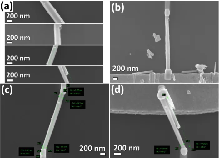
Figure 1a and Figure S1 show SEM images of Au/ZnO NWs with different radius (140,
115, 90 and 60 nm), used in this study in order to investigate the influence of the NW diameter on
the gas sensing properties. All NWs were grown using 0.9 µM of HAuCl4 in electrochemical bath,
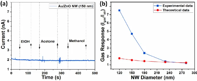
which was demonstrated to be the optimal concentration in order to achieve the highest gas sensing performances [26]. On the surface of all NWs, the Au NPs could be observed (see Figure S2). The gas response at room temperature versus the diameter of the Au/ZnO NW to 100 ppm of hydrogen gas, ethanol, acetone and methanol is presented in Figure 1b. As was demonstrated in our previous work [26], the Au/ZnO NWs are highly selective to hydrogen gas, which can be also observed for NWs in a wide range of radius (from 60 to 140 nm, see Figure 1b), i.e. the selectivity does not depend on the diameter of the NWs. Also, it must be mentioned that for all individual NWs, the number of Au NPs was practically the same (5 ± 3 NPs), in order to exclude the influence of the
7
NP density on the gas response (see Figure 1a and S2). The gas response to 100 ppm of ethanol, acetone and methanol vapors for Au/ZnO NW with 150 nm diameter is presented in Figure S3a, showing no deviation in current values. The gas response of Au/ZnO NWs with radius of 60, 75,
90, 115 and 140 nm to 100 ppm of H2 gas is 7.5, 4.7, 2.4, 1.4 and 1.2, respectively (see Figure
1b).
Figure 1c shows the dynamic gas response at room temperature to 100 ppm of H2 gas of
individual Au/ZnO NWs with different radius (60, 90 and 140 nm). The calculated response and recovery times versus diameter of individual Au/ZnO NW is presented in Figure 1d. A decrease in recovery time with the decrease of the NW diameter can be observed, which is in agreement with other experimental results based on individual semiconducting oxide NWs nanosensors [15, 19]. In the case on Au/ZnO NW with a radius of 60 nm the response and recovery times are 140 s and 300 s, respectively (see Figure 1d).
The rise in H2 gas response by decreasing in NW diameter can be explained based on
increased impact of surface phenomena (adsorption/desorption of gaseous species) on electron transport through the conduction channel of NW [10, 13, 15, 38, 39]. The thinner the NWs, the higher is modulation of surface electron depletion region under adsorption/desorption of oxygen species and then it results in a higher gas response (S) [15]:
2 2 / 1 ) ( 2 2 2 − = − = kT qV D D L D D S air S D air (1)
Assuming that Lgas << D, where D is the diameter of NW, Lair and Lgas are the width of electron
depletion region under air and gas, respectively. λD is the Debye length, T is the absolute
8
under ambient air. According to Eq. (1), the gas response was calculated assuming that Lair is 15
nm [40]. The results in comparison with experimental data are presented in Figure S3b, showing that for relatively thick NWs the experimental data are comparable with theoretical calculations. However, for NWs with radius smaller than 100 nm the experimental data considerably deviate from theoretical results, which may be of high interest for further scientific investigations and new nano-physics. This can be explained based on gas sensing mechanism elaborated in previous work [26], which is based on formation of nanoscale-Schottky contacts at Au NPs/ZnO NW interface
due to higher work function of Au (φAu = 5.1 eV) compared to that of ZnO (φAu = 4.1 eV) [41, 42].
This will lead a to narrower conduction channel (dair) under exposure to ambient air, and therefore
to higher modulation of the conduction channel width (dgas) after exposure to H2 gas (see Figure
2).
Previous studies demonstrated that individual ZnO and doped ZnO NWs (Ag- and Cd-doped) possess a good selectivity to hydrogen gas at room temperature [14, 20-22]. In our case, the surface functionalization with Au NPs induced no changes in the selectivity from hydrogen gas to other tested gases (ethanol, acetone and methanol, see Figure 1b). Thus, we can conclude that the main mechanism responsible for enhancement of gas sensing properties is an additional modulation of the conduction channel due to formation of nanoscale Schottky contacts at the interface of Au NPs and ZnO NWs (or so called electronic sensitization), while catalytic properties of Au NPs do not increase the rate of oxidation of ethanol, acetone or methanol molecules. According to other results, the electronic sensitization does not induce the changes in selectivity and is only responsible for increasing the gas response [43, 44].
9
3.2. Influence of relative humidity on gas sensing properties of individual Au/ZnO nanowires
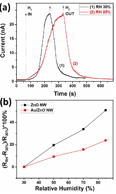
In normal ambient conditions, the value of relative humidity can vary over a wide range, it is thus an important parameter which can reduce the gas sensing properties of metal oxide based gas sensors [45]. Figure 3a shows the dynamic gas response at 30% and 85% RH to 250 ppm of
H2 gas at room temperature for an individual Au/ZnO NW with 75 nm radius. The higher values
of RH were generated using a bubbling system, while the RH value was continuously monitored using a standard hygrometer [34]. It is found that at higher value of RH, the value of the electrical
baseline in the absence of H2 gas, was not clearly modified and that the gas response was slightly
reduced from 35.7 for 30% RH to 32 for 85% RH. In the case of unmodified ZnO NWs (radius of
90 nm) the gas response to 100 ppm of H2 was essentially reduced from 2.3 for 30% RH to 1.2 for
85% RH (see Figure S4). We also observed longer response (~ 190 s) and recovery times (~ 151 s) in the case of exposure in 85% RH, compared to exposure in 30% RH (response time of ~ 76 s and recovery time of ~ 128 s).
The much lower influence of RH on the gas response of a Au-modified ZnO NW can be explained based on a smaller change in resistance under increase in the RH compared to an unmodified ZnO NW. Figure S5 shows the change in resistance of individual Au-modified and unmodified ZnO NWs under the change of the RH value from 30% to 85%. Figure 3b shows the response to RH for devices based on an individual Au-modified and unmodified ZnO NW, based
on measurements from Figure S5. The response was defined as (RRH – R30%)/R30%) · 100%, where
RRH and R30% are the resistance under different values of RH and at 30% RH, respectively. It can
be observed that in the case of the Au-modified ZnO NW the change in resistance by a rise in the RH value is much smaller compared to an unmodified ZnO NW (see Figure 3b), which can explain the lower influence of water vapors on the gas response for the Au-modified ZnO NW. In general, the decrease in resistance of semiconducting oxide under a rise in the RH value can be explained based on hydroxyl poisoning, which was already discussed in other works [34, 45, 46].
10
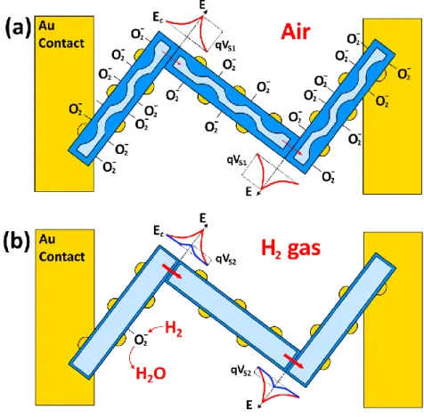
The influence of water vapors on the gas sensing mechanism of the ZnO NW and Au/ZnO NW (presented in cross-section) is tentatively proposed in Figure 4. Under exposure to dry air the
diameter of the conduction channel will be narrowed due to adsorption of oxygen molecules (O2(g)
+ e– → O2(ad) –, see Figure 4a,d) [14, 21]. By exposure of NWs in atmosphere with high
concentration of water vapors, the H2O molecules are adsorbed on the surface of metal oxides in
the molecular or hydroxyl form with donor effect and can replace the previously adsorbed oxygen species by generation of free electrons (see Figure 4b). This leads to a decrease in resistance and
to a widening of the conduction channel (dRH) in the case of a ZnO NW (see Figure 4b) [15, 45].
However, in the case of a Au/ZnO NW we can tentatively propose that Au NPs play the role of hydroxyl adsorbers on the surface of NPs, thereby providing an oxygen adsorption site for surface reactions in humid atmosphere (see Figure 4d,e), which do not lead to the change in the
conduction channel (dair ≈ dRH) [47]. The same effect was observed for Fe2O3-functionalized ZnO
tetrapods [48], Al-doped SnO2 NPs [47], Sb-doped SnO2 [49], CuO-loaded SnO2 hollow spheres
[50], and NiO-doped SnO2 [45]. However, the interactions of water vapors with gold have been
studied by many methods [51-53]. For example, Wells and Fort studied the adsorption of water on clean gold by means of measurement of work function changes, demonstrating that water chemisorbs on the gold with an activation energy of 3 to 9 kcal/mole [51]. Sharma and Thomas measured the adsorption/desorption isotherms of water on the porous plate gold using the quartz crystal sorption (is that correct ??) monitor, showing no strong dependence on the temperature in the range from 22 ºC to 60 ºC [53].
After introduction of H2 gas in the test chamber, the oxidation of H2 molecules will occur
[15, 45]: − − → + +O H O e H2 2(ad) 2 2 2 (2)
Therefore, the electrons will be released back to the NW and will widen the conduction channel (dgas, see Figure 4c,f). However, in the case of a Au/ZnO NW the modulation of conduction
11
channel (dgas - dRH) will be higher due to the non influence of water vapors on the conduction
channel in humid atmosphere. Thus, addition of Au NPs can significantly decrease the influence of water vapors on the gas sensing properties of ZnO NWs, which is very important for practical applications in ambient atmosphere.
3.3. Individual and multiple Au/ZnO NWs based micro- and nanodevices
Figure 5a shows the SEM images of devices based on multiple networked Au/ZnO NWs,
while Figure 5b shows the current – voltage (I – V) characteristics of devices based on individual (radius of 60 nm) and multiple networked Au/ZnO NWs, demonstrating the formation of double asymmetric Schottky contacts. Figure 5a shows that the multiple networked Au/ZnO NWs are connected between the two Au/Cr electrodes using Pt complex contacts deposited in a FIB/SEM system. In the case of multiple NWs the higher current value can be explained based on increased channels for current flow, which was also observed in other experimental results [9, 54].
Figure 5c shows the gas response to 100 ppm of H2 gas at room temperature for single
(with a radius of 60 nm) and multiple Au/ZnO NWs (device from Figure 5a). In the case of multiple NWs higher response value of ~ 40 was obtained, compared to 7.5 for an individual NW.
Figure 5d shows the dynamic gas response at room temperature to different concentrations of H2
gas. The gas response to 30, 50, 100, 150, 175 and 300 ppm is 4.9, 9.6, 40, 50, 55 and 120, respectively (see Figure 5e). The gas response follows a power law relationship on gas
concentration
2 H
p
S , where β ~ 1.1 is the curve slope of the dependence [34]. The theoretical
detection limit of ~ 1 ppm was estimated using signal/noise ratio2, as was reported by Dua et al.
[36], which is smaller value compared to an individual Au/ZnO NW, reported previously [26]. In order to check the reproducibility of a device based on multiple Au/ZnO NWs, three pulses of 300
12
The better gas sensing properties (higher gas response and lower detection limit) of
multiple NWs compared to an individual NW were also observed by Zhang et al. for In2O3 NWs
[9], as well as by Khan et al. for ZnO NWs [54]. We tentatively attribute these improved gas sensing properties to the formation of potential barriers at NW/NW junctions, which is missing in the case of an individual NW [9, 17, 35, 48, 55]. A proposed gas sensing mechanism is presented
in Figure 6. In this case, the modulation of the potential barriers height (qVS1) between Au/ZnO
NWs has the main role in enhancement of the gas sensing properties (see Figure 6) [9, 48, 56, 57]. Under exposure in ambient air, due to adsorbed oxygen species (as was already described in the gas sensing mechanism for individual Au/ZnO NWs in Figure 2) on the surface of Au/ZnO NWs
the electron depletion region will be formed, leading to the formation of potential barriers (qVS1,
see Figure 6a). Under exposure to H2, the width of the electron depletion region is narrowed,
leading to a decrease in the potential barriers height (qVS2, see Figure 6b). In the case of exposure
to H2 gas molecules of the device based on networked NWs the decrease in the barrier height
occurs due to a release of electron after oxidation of the hydrogen molecules [15, 21, 48]:
− − → + + O ad H O e H2 2( ) 2 2 1 (3)
Consequently, the formed additional potential barrier leads to a more efficient modulation in the device resistance [9, 39, 48, 54]. In this case the gas response exponentially depends on the variation of the potential barriers height (qΔVS = qVS1 - qVS2) [58, 59]:
− = air gas S I I kT V q 2 ln (4)
Thus, the device based on multiple networked Au/ZnO NWs demonstrates a more sensitive H2 gas
response compared to the individual NW device.
13
In summary, the individual and multiple networked Au nanoparticles (NPs)-functionalized ZnO nanowires were integrated into nanosensors using a dual beam FIB/SEM system. These devices were studied systematically as gas sensors at room temperature at different RH values.
The nanowire diameter strongly influences the H2 gas sensing properties and we demonstrated that
thinner NWs show a higher gas response and faster response and recovery times at room temperature, which is very important for practical applications. Also, the low impact of water vapors on the sensing properties of an individual Au/ZnO NW was observed, which is very important for operation under ambient conditions. While an individual Au/ZnO NW demonstrated
the response of ~ 7.5 to 100 ppm of H2 gas, the multiple networked NW device showed a higher
gas response of ~ 40. The multiple NWs also demonstrated a smaller theoretical detection limit of ~ 1 ppm at room temperature, compared to ~ 5 ppm for the individual nanowire device. The higher gas response was explained based on a gas sensing mechanism which includes the modulation of a potential barrier height at the interface of different Au/ZnO nanowires bridging external contacts. These results provide useful information for the fabrication of high performance and highly selective H2 gas sensors.
Acknowledgments
Dr. Lupan gratefully acknowledges PSL University, Chimie-ParisTech for invited professor position in 2018 and 2019 and the CNRS Council for support as expert scientist at IRCP Chimie ParisTech, Paris. This research was sponsored partially by the German Research Foundation (DFG) under the schemes FOR 2093 (AD 183/12-2). Katrin Brandenburg is acknowledged for her help in the proof-reading of the manuscript. This research was partly supported by the Technical University of Moldova.
14
References
[1] L. Cao, J.S. White, J.-S. Park, J.A. Schuller, B.M. Clemens, M.L. Brongersma, Engineering Light Absorption in Semiconductor Nanowire Devices, Nature Mater, 8(2009) 643.
[2] Y. Hu, J. Zhou, P.H. Yeh, Z. Li, T.Y. Wei, L. Wang Zhong, Supersensitive, Fast‐Response Nanowire Sensors by Using Schottky Contacts, Adv Mater, 22(2010) 3327-3332.
[3] A. Kolmakov, D.O. Klenov, Y. Lilach, S. Stemmer, M. Moskovits, Enhanced Gas Sensing by Individual SnO2 Nanowires and Nanobelts Functionalized with Pd Catalyst Particles, Nano Lett, 5(2005) 667-673.
[4] A. Kolmakov, Y. Zhang, G. Cheng, M. Moskovits, Detection of CO and O2 Using Tin Oxide Nanowire
Sensors, Adv Mater, 15(2003) 997-1000.
[5] H. Kind, H. Yan, B. Messer, M. Law, P. Yang, Nanowire Ultraviolet Photodetectors and Optical Switches, Adv Mater, 14(2002) 158-160.
[6] E. Strelcov, Y. Lilach, A. Kolmakov, Gas Sensor Based on Metal−Insulator Transition in VO2 Nanowire
Thermistor, Nano Lett, 9(2009) 2322-2326.
[7] F. Hernandez-Ramirez, J.D. Prades, R. Jimenez-Diaz, T. Fischer, A. Romano-Rodriguez, S. Mathur, J.R. Morante, On the Role of Individual Metal Oxide Nanowires in the Scaling Down of Chemical Sensors, Phys Chem Chem Phys, 11(2009) 7105-7110.
[8] L. Peng, L. Hu, X. Fang, Low‐Dimensional Nanostructure Ultraviolet Photodetectors, Adv Mater, 25(2013) 5321-5328.
[9] D. Zhang, Z. Liu, C. Li, T. Tang, X. Liu, S. Han, B. Lei, C. Zhou, Detection of NO2 Down to ppb Levels
Using Individual and Multiple In2O3 Nanowire Devices, Nano Lett, 4(2004) 1919-1924.
[10] F. Hernandez‐Ramirez, D. Prades Joan, A. Tarancon, S. Barth, O. Casals, R. Jimenez‐Diaz, E. Pellicer, J. Rodriguez, R. Morante Joan, A. Juli Miguel, S. Mathur, A. Romano‐Rodriguez, Insight into the Role of Oxygen Diffusion in the Sensing Mechanisms of SnO2 Nanowires, Adv Funct Mater, 18(2008) 2990-2994.
[11] V. Postica, F. Schütt, R. Adelung, O. Lupan, Schottky Diode Based on a Single Carbon–Nanotube– ZnO Hybrid Tetrapod for Selective Sensing Applications, Adv Mater Int, 4(2017) 1700507.
[12] R. Calarco, M. Marso, T. Richter, A.I. Aykanat, R. Meijers, A. v.d. Hart, T. Stoica, H. Lüth, Size-Dependent Photoconductivity in MBE-Grown GaN−Nanowires, Nano Lett, 5(2005) 981-984. [13] J. Gröttrup, V. Postica, N. Ababii, O. Lupan, C. Zamponi, D. Meyners, Y.K. Mishra, V. Sontea, I. Tiginyanu, R. Adelung, Size-Dependent UV and Gas Sensing Response of Individual Fe2O3-ZnO:Fe Micro-
and Nanowire Based Devices, J Alloys Comp, 701(2017) 920-925.
[14] O. Lupan, L. Chow, T. Pauporté, L.K. Ono, B. Roldan Cuenya, G. Chai, Highly Sensitive and Selective Hydrogen Single-Nanowire Nanosensor, Sens Actuators B, 173(2012) 772-780.
[15] O. Lupan, V. Postica, F. Labat, I. Ciofini, T. Pauporté, R. Adelung, Ultra-Sensitive and Selective Hydrogen Nanosensor with Fast Response at Room Temperature Based on a Single Pd/ZnO Nanowire, Sens Actuators B, 254(2018) 1259-1270.
[16] S. Mathur, S. Barth, H. Shen, J.C. Pyun, U. Werner, Size‐Dependent Photoconductance in SnO2
Nanowires, Small, 1(2005) 713-717.
[17] F. Schütt, V. Postica, R. Adelung, O. Lupan, Single and Networked ZnO–CNT Hybrid Tetrapods for Selective Room-Temperature High-Performance Ammonia Sensors, ACS Appl Mater Interfaces, 9(2017) 23107-23118.
[18] F. Yang, S.-C. Kung, M. Cheng, J.C. Hemminger, R.M. Penner, Smaller is Faster and More Sensitive: The Effect of Wire Size on the Detection of Hydrogen by Single Palladium Nanowires, ACS Nano, 4(2010) 5233-5244.
[19] M. Tonezzer, N.V. Hieu, Size-Dependent Response of Single-Nanowire Gas Sensors, Sens Actuators B, 163(2012) 146-152.
[20] O. Lupan, G. Chai, L. Chow, Fabrication of ZnO Nanorod-Based Hydrogen Gas Nanosensor, Microelectron J, 38(2007) 1211-1216.
[21] O. Lupan, V. Cretu, V. Postica, M. Ahmadi, B.R. Cuenya, L. Chow, I. Tiginyanu, B. Viana, T. Pauporté, R. Adelung, Silver-Doped Zinc Oxide Single Nanowire Multifunctional Nanosensor with a Significant Enhancement in Response, Sens Actuators B, 223(2016) 893-903.
15
[22] O. Lupan, V.V. Ursaki, G. Chai, L. Chow, G.A. Emelchenko, I.M. Tiginyanu, A.N. Gruzintsev, A.N. Redkin, Selective Hydrogen Gas Nanosensor Using Individual ZnO Nanowire with Fast Response at Room Temperature, Sens Actuators B, 144(2010) 56-66.
[23] O. Lupan, V. Postica, R. Adelung, F. Labat, I. Ciofini, U. Schürmann, L. Kienle, L. Chow, B. Viana, T. Pauporté, Functionalized Pd/ZnO Nanowires for Nanosensors, Phys Status Solidi (RRL), 12(2017) 1700321.
[24] N. Yamazoe, New Approaches for Improving Semiconductor Gas Sensors, Sens Actuators B, 5(1991) 7-19.
[25] L. Liao, H.X. Mai, Q. Yuan, H.B. Lu, J.C. Li, C. Liu, C.H. Yan, Z.X. Shen, T. Yu, Single CeO2 Nanowire Gas
Sensor Supported with Pt Nanocrystals: Gas Sensitivity, Surface Bond States, and Chemical Mechanism, J Phys Chem C, 112(2008) 9061-9065.
[26] O. Lupan, V. Postica, T. Pauporté, R. Adelung, Synthesis of Au-Modified ZnO NWs for Ultra-Sensitive Gas Nanosensor, ACS Appl Mater Interfaces, In progress, (2019).
[27] Z. Feng, Y. Ma, V. Natarajan, Q. Zhao, X. Ma, J. Zhan, In-Situ Generation of Highly Dispersed Au Nanoparticles on Porous ZnO Nanoplates via Ion Exchange from Hydrozincite for VOCs Gas Sensing, Sens Actuators B, 255(2018) 884-890.
[28] N. Gogurla, A.K. Sinha, S. Santra, S. Manna, S.K. Ray, Multifunctional Au-ZnO Plasmonic
Nanostructures for Enhanced UV Photodetector and Room Temperature NO Sensing Devices, Sci Rep, 4(2014) 6483.
[29] J. Guo, J. Zhang, M. Zhu, D. Ju, H. Xu, B. Cao, High-Performance Gas Sensor Based on ZnO Nanowires Functionalized by Au Nanoparticles, Sens Actuators B, 199(2014) 339-345.
[30] H.E. Belghiti, T. Pauporté, D. Lincot, Mechanistic Study of ZnO Nanorod Array Electrodeposition, phys status solidi (a), 205(2008) 2360-2364.
[31] O. Lupan, T. Pauporté, Hydrothermal Treatment for the Marked Structural and Optical Quality Improvement of ZnO Nanowire Arrays Deposited on Lightweight Flexible Substrates, J Cryst Growth, 312(2010) 2454-2458.
[32] O. Lupan, V. Cretu, M. Deng, D. Gedamu, I. Paulowicz, S. Kaps, Y.K. Mishra, O. Polonskyi, C. Zamponi, L. Kienle, V. Trofim, I. Tiginyanu, R. Adelung, Versatile Growth of Freestanding Orthorhombic α-Molybdenum Trioxide Nano- and Microstructures by Rapid Thermal Processing for Gas Nanosensors, J Phys Chem C, 118(2014) 15068-15078.
[33] O. Lupan, V. Postica, N. Wolff, O. Polonskyi, V. Duppel, V. Kaidas, E. Lazari, N. Ababii, F. Faupel, L. Kienle, R. Adelung, Localized Synthesis of Iron Oxide Nanowires and Fabrication of High Performance Nanosensors Based on a Single Fe2O3 Nanowire, Small, 13(2017) 1602868.
[34] V. Cretu, V. Postica, A.K. Mishra, M. Hoppe, I. Tiginyanu, Y.K. Mishra, L. Chow, N.H. de Leeuw, R. Adelung, O. Lupan, Synthesis, Characterization and DFT Studies of Zinc-Doped Copper Oxide
Nanocrystals for Gas Sensing Applications, J Mater Chem A, 4(2016) 6527-6539.
[35] O. Lupan, V. Postica, V. Cretu, N. Wolff, V. Duppel, L. Kienle, R. Adelung, Single and Networked CuO Nanowires for Highly Sensitive p‐Type Semiconductor Gas Sensor Applications, Phys Status Solidi (RRL) 10(2015) 260-266.
[36] V. Dua, P. Surwade Sumedh , S. Ammu, S.R. Agnihotra, S. Jain, E. Roberts Kyle , S. Park, S. Ruoff Rodney , K. Manohar Sanjeev All‐Organic Vapor Sensor Using Inkjet‐Printed Reduced Graphene Oxide, Angew Chem, Int Ed, 49(2010) 2154-2157.
[37] J. Li, Y. Lu, Q. Ye, M. Cinke, J. Han, M. Meyyappan, Carbon Nanotube Sensors for Gas and Organic Vapor Detection, Nano Lett, 3(2003) 929-933.
[38] L. Liao, H.B. Lu, J.C. Li, H. He, D.F. Wang, D.J. Fu, C. Liu, W.F. Zhang, Size Dependence of Gas Sensitivity of ZnO Nanorods, J Phys Chem C, 111(2007) 1900-1903.
[39] I. Paulowicz, V. Postica, O. Lupan, N. Wolff, S. Shree, A. Cojocaru, M. Deng, Y.K. Mishra, I. Tiginyanu, L. Kienle, R. Adelung, Zinc Oxide Nanotetrapods with Four Different Arm Morphologies for Versatile Nanosensors, Sens Actuators B, 262(2018) 425-435.
[40] Z. Fan, D. Wang, P.-C. Chang, W.-Y. Tseng, J.G. Lu, ZnO Nanowire Field-Effect Transistor and Oxygen Sensing Property, Appl Phys Lett, 85(2004) 5923-5925.
[41] K. Liu, M. Sakurai, M. Liao, M. Aono, Giant Improvement of the Performance of ZnO Nanowire Photodetectors by Au Nanoparticles, J Phys Chem C, 114(2010) 19835-19839.
16
[42] K. Joondong, Y. Ju-Hyung, K. Chang Hyun, P. Yun Chang, W. Ju Yeon, P. Jeunghee, L. Jung-Ho, Y. Junsin, H. Chang-Soo, ZnO Nanowire-Embedded Schottky Diode for Effective UV Detection by the Barrier Reduction Effect, Nanotechnol, 21(2010) 115205.
[43] S.-W. Choi, A. Katoch, J.-H. Kim, S.S. Kim, Remarkable Improvement of Gas-Sensing Abilities in p-type Oxide Nanowires by Local Modification of the Hole-Accumulation Layer, ACS Appl Mater Interfaces, 7(2015) 647-652.
[44] D.R. Miller, S.A. Akbar, P.A. Morris, Nanoscale Metal Oxide-Based Heterojunctions for Gas Sensing: A Review, Sens Actuators B, 204(2014) 250-272.
[45] H.R. Kim, A. Haensch, I.D. Kim, N. Barsan, U. Weimar, J.H. Lee, The Role of NiO Doping in Reducing the Impact of Humidity on the Performance of SnO2‐Based Gas Sensors: Synthesis Strategies, and
Phenomenological and Spectroscopic Studies, Adv Funct Mater, 21(2011) 4456-4463.
[46] O. Lupan, V. Cretu, V. Postica, O. Polonskyi, N. Ababii, F. Schütt, V. Kaidas, F. Faupel, R. Adelung, Non-Planar Nanoscale p–p Heterojunctions Formation in ZnxCu1−xOy Nanocrystals by Mixed Phases for
Enhanced Sensors, Sens Actuators B, 230(2016) 832-843.
[47] K. Suematsu, N. Ma, M. Yuasa, T. Kida, K. Shimanoe, Surface-Modification of SnO2 Nanoparticles by
Incorporation of Al for the Detection of Combustible Gases in a Humid Atmosphere, RSC Adv, 5(2015) 86347-86354.
[48] O. Lupan, V. Postica, J. Gröttrup, A.K. Mishra, N.H. de Leeuw, R. Adelung, Enhanced UV and Ethanol Vapour Sensing of a Single 3-D ZnO Tetrapod Alloyed with Fe2O3 Nanoparticles, Sens Actuators B,
245(2017) 448-461.
[49] K. Suematsu, M. Sasaki, N. Ma, M. Yuasa, K. Shimanoe, Antimony-Doped Tin Dioxide Gas Sensors Exhibiting High Stability in the Sensitivity to Humidity Changes, ACS Sens, 1(2016) 913-920.
[50] K.-I. Choi, H.-J. Kim, Y.C. Kang, J.-H. Lee, Ultraselective and Ultrasensitive Detection of H2S in Highly
Humid Atmosphere Using CuO-Loaded SnO2 Hollow Spheres for Real-Time Diagnosis of Halitosis, Sens
Actuators B, 194(2014) 371-376.
[51] R.L. Wells, T. Fort, Adsorption of water on clean gold by measurement of work function changes, Surf Sci, 32(1972) 554-560.
[52] M. Hakamada, N. Kato, N. Miyazawa, M. Mabuchi, Water-adsorption effect on electrical resistivity of nanoporous gold, Scr Mater, 123(2016) 30-33.
[53] S.P. Sharma, J.H. Thomas Iii, Adsorption of water vapor on thin‐gold electroplate on copper, Journal of Vacuum Science and Technology, 14(1977) 825-827.
[54] R. Khan, H.W. Ra, J.T. Kim, W.S. Jang, D. Sharma, Y.H. Im, Nanojunction Effects in Multiple ZnO Nanowire Gas Sensor, Sens Actuators B, 150(2010) 389-393.
[55] O. Lupan, V. Postica, J. Marx, M. Mecklenburg, Y.K. Mishra, K. Schulte, B. Fiedler, R. Adelung, Individual Hollow and Mesoporous Aero-Graphitic Microtube Based Devices for Gas Sensing Applications, Appl Phys Lett, 110(2017) 263109.
[56] V. Postica, J. Gröttrup, R. Adelung, O. Lupan, K. Mishra Abhishek, H. de Leeuw Nora, N. Ababii, F.C. Carreira José, J. Rodrigues, B. Sedrine Nebiha, R. Correia Maria, T. Monteiro, V. Sontea, K. Mishra
Yogendra, Multifunctional Materials: A Case Study of the Effects of Metal Doping on ZnO Tetrapods with Bismuth and Tin Oxides, Adv Funct Mater, 27(2016) 1604676.
[57] V. Postica, M. Hoppe, J. Gröttrup, P. Hayes, V. Röbisch, D. Smazna, R. Adelung, B. Viana, P. Aschehoug, T. Pauporté, O. Lupan, Morphology Dependent UV Photoresponse of Sn-Doped ZnO Microstructures, Solid State Sci, 71(2017) 75-86.
[58] N. Bârsan, M. Hübner, U. Weimar, Conduction Mechanisms in SnO2 Based Polycrystalline Thick Film
Gas Sensors Exposed to CO and H2 in Different Oxygen Backgrounds, Sens Actuators B, 157(2011)
510-517.
[59] V. Postica, I. Hölken, V. Schneider, V. Kaidas, O. Polonskyi, V. Cretu, I. Tiginyanu, F. Faupel, R. Adelung, O. Lupan, Multifunctional Device Based on ZnO:Fe Nanostructured Films with Enhanced UV and Ultra-Fast Ethanol Vapour Sensing, Mater Sci Semicon Proc, 49(2016) 20-33.
17
Figure 1. (a) SEM image of an individual Au/ZnO nanowire with a radius of 140 nm. (b) Gas
response at room temperature versus diameter of Au/ZnO NWs to 100 ppm of H2 gas and different
volatile organic compounds. (c) Dynamic gas response for Au/ZnO nanowires with a radius of 60,
90 and 140 nm to 100 ppm of H2 gas. (d) The calculated response and recovery times to 100 ppm
18
Figure 2. Illustration of the gas sensing mechanism for an individual Au/ZnO nanowire under
exposure to ambient air and H2 gas in the case of a relatively smaller diameter (a); and a relatively
19
Figure 3. (a) Dynamic gas response at 30% and 85% RH to 250 ppm of H2 for a Au/ZnO nanowire
with 75 nm radius. (b) The response to RH for an unmodified and a modified individual ZnO nanowire.
20
Figure 4. Schematic illustration of the water vapors influence on the gas sensing mechanism of a
ZnO (a-c) and a Au/ZnO NW (d-f) at room temperature: (a,d) exposure under air; (b,e) exposure
under atmosphere with high concentration of water vapors RH; (c,f) introduction of H2 gas
21
Figure 5. (a) SEM image of a device based on multiple Au/ZnO nanowires. (b) Current – voltage
characteristics for a single Au/ZnO nanowire and multiple Au/ZnO nanowires. (c) Room temperature gas response for single and multiple Au/ZnO NWs. (d) Dynamic response of a device
based on multiple NWs to different concentrations of H2 gas at room temperature. (e) Dependence
of the gas response on the H2 gas concentration for multiple nanowires. (f) Room temperature gas
22
Figure 6. Illustration of the gas sensing mechanism for multiple networked Au/ZnO nanowires
23
Supporting Information for
Room temperature gas nanosensors based on individual
and multiple networked Au-modified ZnO nanowires
Oleg Lupan,1,2,3,* Vasile Postica,2 Thierry Pauporté,3 Bruno Viana,3 Maik-Ivo Terasa,1 Rainer Adelung,1
1 Functional Nanomaterials, Faculty of Engineering, Institute for Materials Science, Kiel University,
Kaiserstr. 2, D-24143, Kiel, Germany
2 Center for Nanotechnology and Nanosensors, Department of Microelectronics and Biomedical
Engineering, Technical University of Moldova, 168 Stefan cel Mare Av., MD-2004 Chisinau, Republic of Moldova
3 PSL Université, Institut de Recherche de Chimie Paris, ChimieParisTech, UMR CNRS 8247, 11 rue
Pierre et Marie Curie 75231 Paris cedex 05, France
*Corresponding authors
Prof. Dr. Eng. Lupan, Prof. Dr. Adelung E-mails: ollu@tf.uni-kiel.de ra@tf.uni-kiel.de Institute for Materials Science, Kiel University, Germany
Prof. Dr. Thierry Pauporté E-mail: thierry.pauporte@chimieparistech.psl.eu
PSL Université, ChimieParisTech, France
24
Figure S1. Schematic illustration of the chip used for the fabrication of the nanosensors: (a) overall
view, (b) top view (with red dotted circles the regions where the structures can be integrated are indicated) and (c) front view.
25
Figure S2. (a) Comparative SEM images of a small area of individual Au/ZnO NWs with different
diameters integrated into the devices. SEM images of the devices based on individual Au/ZnO NWs with a radius of: (b) 125, (c) 90 and (d) 60 nm.
26
Figure S3. Dynamic response at room temperature of a Au/ZnO NW with 75 nm radius to different
vapors of VOCs. (b) The experimental and calculated gas response (using Eq. 1) versus the diameter of the Au/ZnO NW.
27
Figure S4. Dynamic gas response at 30% and 85% RH to 100 ppm of H2 gas for an individual
28
Figure S5. The dependence of resistance for individual unmodified and Au-modified ZnO NWs