HAL Id: hal-02988734
https://hal.archives-ouvertes.fr/hal-02988734
Submitted on 4 Nov 2020HAL is a multi-disciplinary open access
archive for the deposit and dissemination of sci-entific research documents, whether they are pub-lished or not. The documents may come from teaching and research institutions in France or abroad, or from public or private research centers.
L’archive ouverte pluridisciplinaire HAL, est destinée au dépôt et à la diffusion de documents scientifiques de niveau recherche, publiés ou non, émanant des établissements d’enseignement et de recherche français ou étrangers, des laboratoires publics ou privés.
Impact of Electron–Phonon Scattering on Optical
Properties of CH3NH3PbI3 Hybrid Perovskite Material
Benoit Galvani, Daniel Suchet, Amaury Delamarre, Marc Bescond, Fabienne
Michelini, Michel Lannoo, Jean-François Guillemoles, Nicolas Cavassilas
To cite this version:
Benoit Galvani, Daniel Suchet, Amaury Delamarre, Marc Bescond, Fabienne Michelini, et al.. Im-pact of Electron–Phonon Scattering on Optical Properties of CH3NH3PbI3 Hybrid Perovskite Ma-terial. ACS Omega, ACS Publications, 2019, 4, pp.21487 - 21493. �10.1021/acsomega.9b03178�. �hal-02988734�
Impact of Electron
−Phonon Scattering on Optical Properties of
CH
3
NH
3
PbI
3
Hybrid Perovskite Material
Benoit Galvani,
†Daniel Suchet,
‡Amaury Delamarre,
§Marc Bescond,
∥Fabienne Velia Michelini,
†Michel Lannoo,
†Jean-Francois Guillemoles,
⊥and Nicolas Cavassilas
*
,††Aix Marseille Université, CNRS, Université de Toulon, IM2NP UMR 7334, 13397 Marseille, France ‡Ecole Polytechnique, IPVF, Institut Photovoltaque d’ Ile-de-France, 30 RD 128, 91120 Palaiseau, France §Centre de Nanosciences et de Nanotechnologies, 91120 Palaiseau, Ile-de-France, France
∥LIMMS, CNRS-Institute of Industrial Science, UMI 2820, University of Tokyo, 153-8505 Tokyo, Japan ⊥IPVF, Institut Photovoltaque d’ Ile-de-France, 30 RD 128, 91120 Palaiseau, France
*
S Supporting InformationABSTRACT: We numerically investigate the impact of electron−phonon scattering on the optical properties of a perovskite material (CH3NH3PbI3). Using nonequilibrium Green function formalism, we calculate the local density of states for several values of the electron−phonon scattering strength. We report an Urbach-like penetration of the density of states in the band gap due to scattering. A physical analytical model allows us to attribute this behavior to a multiphonon process. Values of Urbach energy up to 9.5 meV are obtained, meaning that scattering contribution to the total experimental Urbach energy of 15 meV is quite important. We also show that the open-circuit voltage Voc, for a solar cell
assuming such a material as an absorber, depends on the scattering strength. Vocloss increases with the scattering strength, up to 41 mV. Finally, an unexpected result of this study, is that the impact of electron−phonon scattering on Urbach tail and Voc
increases with the phonon energy. This low value in perovskite (8 meV) is therefore an advantage for photovoltaic applications.
■
INTRODUCTIONPerovskite materials are widely studied for both device conception and theoretical understanding. Among the variety of perovskites materials, organic−inorganic hybrid perovskites are the most promising materials for optoelectronic applica-tions. First, photovoltaic cells made of hybrid perovskites lacked stability and had a low solar conversion efficiency, of the order 3%. Nowadays, fabrication techniques of perovskites have been largely improved, making them more stable and reliable to use in solar cells. Production costs have also been drastically reduced, paving the way to further decrease the PV electricity price.1This fast evolution of technology has led to an increase of efficiency, up to 24% in less than 10 years,2and have reached over 28% in Si-perovskite tandem devices.3
Hybrid perovskite represents one of the most promising materials for reliable solar conversion technology, thanks to their excellent optical and electrical properties. They exhibit high carrier diffusion lengths, reaching up to 1 μm even in nanostructures.4 High carrier lifetime has also been measured to be around several microseconds.5 Moreover, it has been shown that hybrid perovskites have remarkable photon absorption properties.6 These properties have also been observed in perovskite layers as thin as 50 nm.7 The main advantage of such thinfilms is to be integrated in lightweight,
flexible, and transparent solar cells8
that couldfind applications in wearable electronics.
However, remarkable properties of these materials cannot be fully understood considering the peculiar structure of hybrid perovskites. On the one hand, with these excellent carrier-transport properties, we could expect hybrid perovskites to exhibit high carrier mobilities. Yet, several groups have reported low values for carrier mobilities in perovskite-based devices. Mei et al. found mobilities of 1 cm2/(V s) in a
field-effect transistor.9Shi et al. estimated the electron mobility in a single crystal to be 115 cm2/(V s)10 Microwave conductivity measurements gave carrier mobilities from 6 to 60 cm2/(V s).11,12 These measured values are quite low compared to mobilities in other inorganic materials used in PV cells (electron mobility is equal to 1500 cm2/(V s) in silicon) and could indicate some disorder in the crystalline structure. On the other hand, it is possible to extract information about the quality of the material from the absorption features below the band gap. The Urbach rule gives the absorption coefficient
Received: September 27, 2019
Accepted: November 15, 2019
Published: December 5, 2019
Article http://pubs.acs.org/journal/acsodf
Cite This:ACS Omega 2019, 4, 21487−21493
copying and redistribution of the article or any adaptations for non-commercial purposes.
Downloaded via 78.193.74.156 on May 10, 2020 at 22:39:13 (UTC).
below the band gap as a function of photon energy and temperature. It is described by a“tail” with the expression
h h E E ( ) 0exp g U α ν =α ν− Ä Ç ÅÅÅÅÅ ÅÅÅÅÅ É Ö ÑÑÑÑÑ ÑÑÑÑÑ (1)
whereα0is a constant, Eg is the material band gap, hν is the
incident photon energy, and EU is the Urbach energy, corresponding to the width of the exponential part of the absorption below the band gap. This empirical formula is an important tool to study the optical absorption due to its simplicity and applicability for various types of materials and structures. This phenomenon has three principal physical causes which are the crystal disordering,13trap states due to impurities14 and electron−phonon scattering (EPS).15,16 Depending on the type of material, one of these causes dominates. In amorphous material, the Urbach energy, which can reach up to 50 meV,17is mainly due to disordering, while in well-ordered materials like GaAs, the Urbach energy, which is as low as 7.5 meV,18,19is mainly due to the EPS. In the case of hybrid perovskite-based device, the Urbach energy has been estimated experimentally to be 15 meV.20However, the origin of this band tail is still debated in the literature. In ref21, the authors attribute the latter to the presence of trap states in the band gap. The understanding of this behavior is important since it modifies the characteristic of the corresponding solar cell with a Stokes shift and impacts the open-circuit voltage Voc.22 The definition of the optical band gap can also be discussed.23,24
In hybrid perovskites, the scattering with polar optical phonons is expected to be large since (i) the difference between ϵ∞ and ϵstat (the dynamic and the static dielectric constant respectively) is large25 and (ii) the small phonon energy implies a large number of phonons (all parameters are reported in Table 1). Moreover, rotations of the CH3NH3
organic matrix may play a key role in quantum transport properties.26 Random rotations of cations inducefluctuations of the electrostatic potential. Electrons and holes in the material become localized and spatially separated, affecting their transport properties and the corresponding mobilities. It can then be expected that EPS also impacts the Urbach tail.
Numerical study of Urbach tail assumes that the acoustic phonon has already been conducted.16 Recently, using nonequilibrium Green’s functions (NEGF) formalism,27 impurities and EPS have been considered to allow to reproduce the band tail and the band gap narrowing in a nanowire. Using the same formalism,28in the present work, we numerically study the impact of the polar optical phonon on the optical and electrical properties of hybrid perovskite materials. We show that such an interaction modifies the electronic density of states (DOS), leading to the enhancement of an Urbach tail in the band gap. To better interpret our results, we develop an original analytical model of the DOS in
the band gap. This model is in good agreement with the numerical results assuming only well-known material param-eters such as effective masses, electron−phonon coupling, and phonon energy. It also allows to illustrate that the Urbach tail due to polar optical phonon is related to a multiphonon process. Finally, calculations of the absorption and the emission current contributions allow to estimate the variation of Vocwith respect to the EPS strength.
■
METHODOLOGYTo study the impact of EPS, we made numerical calculations using NEGF formalism within the self-consistent Born approximation.29 This model is detailed in ref 28, but we recall here the main elements needed for an easier under-standing. We consider a three-dimensional (3D) device, with wide transverse dimensions perpendicular to the transport axis. This allows to assume a one-dimensional (1D) model in the longitudinal direction for each transverse mode corresponding to a propagation in the transverse plane with a given transverse wave vector. In our case, we consider Nkt = 30 transverse
modes. For each mode, we define a Hamiltonian Hkt, in the 1D site basis using the effective mass approximation, which is suitable for the study of most crystalline material, including perovskite.30This allows to calculate the corresponding lesser G<(E, k
t) and greater G>(E, kt) Green’s functions, relative to
electron and hole densities, respectively. The DOS in both conduction and valence bands is given by the retarded Green function GR(E, kt). We consider the diagonal approximation to
describe the EPS and assume the effective mass approximation for both conduction and heavy-hole valence bands. To make the calculations with such formalism, we need to take the band diagram of the device as well as the EPS strength and phonon density as input data in our code. For calculations in a solar cell, the band diagram, relative to electricfield and band offset, is obtained by the Poisson−Schrödinger self-consistent approach. To do so, we implemented the structure in SCAPS software.31 SCAPS is a solar cell simulation program that calculates the optical and electronic characteristics of multilayer semiconductor devices based on a drift-diffusion model. In our case, we have used SCAPS to extract data relative to the band diagram of our device as an inputfile of our Green’s function simulations.
In such a polar material, polar optical phonons dominate the carrier transport. While the model of Sarangapani et al. includes scatterings with both polar optical phonon and charged impurities, and Grein et al. assumed only acoustic phonons, we then only assume the polar optical phonons. The strength of this electron−phonon interaction is given by
M C S E 1 2 4 1 1 pop EPS pop 0 stat π π = ϵ ϵ∞ − ϵ i k jjjjj y{zzzzz (2)
where S is the surface of the transverse cross section of radius R = 30 nm; Epop is the polar optical phonon energy of the
material;ϵ0is the vacuum permittivity; andϵ∞andϵstatare the relative dynamic and static permittivities, respectively. All used parameters are given in Table 2. CEPS is a numerical fitting factor, which is adjusted to a value such that the model accounts for the correct value of the electron mobility.32The relation between CEPS and mobility is shown in Table 2.
Electron mobility in hybrid perovskites has been experimen-tally measured from 1 to 100 cm2/(V s). Mechanisms Table 1. Constant Parameters of CH3NH3PbI3
parameter value me*/m0 0.23 mh*/m0 0.17 ϵ∞ 6.0 ϵstat 29.0 Epop(meV) 8.0
ACS Omega Article
DOI:10.1021/acsomega.9b03178
ACS Omega 2019, 4, 21487−21493
controlling the carrier mobility in this material are not clearly understood, since the CH3NH3molecular rotations could have
an impact on carrier-transport properties.26From a formalism point of view, these rotations are close to the electron−phonon interaction, but with unknown parameters. In the following, we perform calculations with 4 different values of CEPS
corresponding to mobilities ranging from 0.13 to 86 cm2/(V s) as reported in the literature.
The number of phonons per unit cell5pop is given by the Bose−Einstein distribution
( )
E T ( , ) 1 exp E 1 k TB 5 = − (3)where E = Epop= 8 meV and T = 300 K in the case of phonons
in CH3NH3PbI3. Since Epop is small in the considered
perovskite material (compared to kBT = 25.7 meV and
compared for example to the GaAs value of 35 meV),5pop is large. We consider the EPS by calculating the corresponding interaction self-energies E k E M k k G E E k G E E k M k k ( , , ) ( , ) ( , ) ( 1) ( , ) ( , ) t k t t t t t t t t
pop pop pop pop
pop pop t 5 5
∑
Σ = ′ [ − ′ + + + ′ ] ′ < ′ < < (4) E k E M k k G E E k G E E k M k k ( , , ) ( , ) ( , ) ( 1) ( , ) ( , ) t k t t t t t t t tpop pop pop pop
pop pop t 5 5
∑
Σ = ′ [ + ′ + + − ′ ] ′ < ′ > > (5)where Mt(kt, kt′) is the intermode coupling matrix, which
depends on both considered modes ktand kt′and on Mpop.33
Equation 4describes the interaction with electrons, whileeq 5
accounts for those with holes. Terms in 5pop correspond to
phonon absorption, while terms in(5 +pop 1) correspond to phonon emission. Calculations of energies are self-consistent, since G< and G> also depend on these
self-energies28
NEGF calculations allow us to estimate the current generated by the cell in the dark as well as under illumination. From current calculations, we can thus deduce the relation between Vocand EPS.
The electrical characteristic of a solar cell is close to the diode characteristic. In the dark, the current generated by the cell is given by I qV k T exp 1 dark 0 B 0 = − Ä Ç ÅÅÅÅÅ ÅÅÅÅÅ ikjjjjj y { zzzzz ÉÖÑÑÑÑÑÑÑÑÑÑ (6)
where I0is the current relative to recombination of majority carriers in the cell for a bias V = 0 V. In the dark, I0
compensates the minority carrier current and the total current is zero. Under illumination, the current in the cell at a bias V can be estimated by
I
light sc dark
0 = − +0 (7)
where Iscis the short-circuit current of the cell, which is the
photocurrent at zero bias. Here, we consider that the photocurrent does not depend on the bias V. It is then possible to estimate the open-circuit voltage Voconly with the Green’s functions calculated at V = 0 V
V k T I I ln oc B sc 0 = i k jjjjj y{zzzzz (8)
Voc is calculated for each value of CEPS, and each Voc is compared to the ballistic counterpart (CEPS = 0) to estimate
δVoc, the losses due to EPS. Iscand I0are calculated using
I I h h q h G E k G E h k h T E h ( )d ( ) ( , ) ( , ) ( , ) d d h k E h c v t t sc sc sun t * 5
∫
∫ ∫
∑
ν ν ρ ν ν ν ν = = Ω + ν ν − < > (9) and I q h G E h k G E k E h ( ) ( , ) ( , ) d d k E h c v t t 0 t *∫ ∫
∑
ρ ν ν ν = Ω + ν − < > (10)where *c v−( )hν is a band coupling parameter,34 E is the electron energy, hν is the photon energy, and Ω is the solid angle of the light source, which is equal to 6.79× 10⁻⁵sr for Isc
andπ sr for I0.5 ν(h ,Tsun)is the Bose−Einstein distribution of
photons (seeeq 3) at the energy hν and temperature Tsun=
6000 K andρ(hν) iss the photon DOS per unit energy and unit volume h hc h ( ) 8 ( )3( ) 2 ρ ν = π ν (11)
I0depends on G<(E + hν) and G>(E), which are the electron
density at energy E + hν and the hole density at energy E, respectively. An electron in the conduction band can recombine with a hole in the valence band, emitting a photon of energy hν. On the other hand,eq 9shows that Iscdepends
on G<(E) and G>(E + hν), which are the electron density at
energy E and the hole density at energy E + hν. An electron in the valence band can interact with a photon with energy hν to populate a state in the conduction band.
■
RESULTS AND DISCUSSIONDensity of States. Figure 1 shows the local DOS calculated in a solar cell with an hybrid perovskite active region. We performed the calculations with a CEPS
correspond-ing to an electron mobility of 86 cm2/(V s) and in the ballistic
approximation (CEPS= 0). The two situations are compared in
Figure 1. In the ballistic case, quantum tunneling leads to a small butfinite penetration of the DOS in the band gap. This DOS distribution has been shown to impact the optical properties of ultrathin solar cells.35 By comparison, the Table 2. Numerical Values of the Scattering Strength
Multiplicative Coefficient, with the Estimated Electron Mobility and Calculated Urbach Energy
CEPS μe−(cm2/(V s)) E U(meV) 1.6 86 5.25 5.0 18 6.6 10.0 1.7 7.9 20.0 0.13 9.5
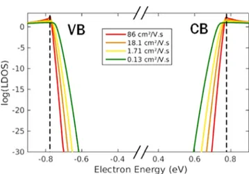
presence of EPS strongly enforces the penetration of DOS within the band gap, which largely dominates the one induced by quantum tunneling. The presence of these near-band-edge states allow both electrons and holes to be either photo-generated or recombined at energies lower than the material band gap of 1.55 eV. To illustrate the evolution of broadening with the interaction strength, we have also made local DOS calculations for each value of the scattering strength.Figure 2
shows these DOS in the middle of the device versus the electron energy. The DOS tends to penetrate deeper in the band gap as the EPS becomes stronger.
To get some physical insight, we developed an analytic model showing the relative importance of the various parameters. The gap density of states is related to the imaginary part of the retarded Green’s function
D E G E E ( ) 1 2 Im( ) ( ) k k k k R 2 2 t t t t π = = Γ − + Γ (12)
where Ektis the energy of the band edge (we consider here the
conduction band) and k 1 Im( )
2 R
t
Γ = π Σ . Usingeqs 4and5and the approach developed in ref 33, we can write Γkt in a continuous form M d k k k D E E D E E (2 ) ( ) ( 1) ( ) k t t t t k k 3 3 2 pop pop pop pop t t t 5 5
∫
π Γ = ′ | − ′| [ ′ + + + ′ − ] (13)which is valid for small electron concentrations. As shown in the Supporting Information (eqs S5 and S9), this set of equations can be reduced to
D E E E E E D E E D E E ( ) ( ) ( ) ( 1) ( ) M 0 02 3/2
pop 0 pop pop 0 pop t 5 5 = Γ = [ + + + − ] i k jjjj y{zzzz (14) withEM3/2 0.02Mt2
( )
2m t = 2 * ℏ .This is a set of ladder equations, which are related to multiphonon process, leading to an exponential decrease of large negative energies. In this regime,|E| ≫ Epop andeq 14
become a simple differential equation, valid at large E Epop
| |
. To solve it, we use the expected exponential behavior by writing D(E) = A exp(σ(E)) and incorporate it into eq 14 together with afirst-order expansion σ(E ± Epop) = σ(E) ± σ′(E)Epop. With this, all terms in σ(E) disappear and, by expanding exp(±σ′(E)Epop) to second order and keeping the dominant term in|E|, one gets
E E E E ( ) 2 2 1 M pop pop 3/4 t 5 σ′ = + | | i k jjjjj j y { zzzzz z i k jjjjj j y { zzzzz z (15)
whose integration gives
D E E E E ln( ) 2 2 1 4 7 ( ) Cte M 0 pop g7/4 pop 3/4 t 5 σ = = − + − + i k jjjjj j y { zzzzz z (16)
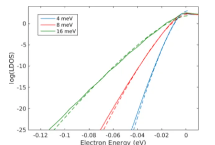
This depends upon two basic parameters Epopand EMt. Note
that it depends upon 1/Mtlinearly. This analytical expression is compared to the full numerical result in Figures 3 and 4, showing an excellent agreement at large energies, apart from a shift due to the constant. In particular, we confirm that the
Figure 1.Local density of states in a perovskite-based device (shown above) as a function of position and electron energy, calculated (a) with electron−phonon interaction and (b) without electron−phonon interaction.
Figure 2.Logarithm of the density of states as a function of electron energy at afixed position in the middle of the active region of the perovskite-based device. Each color corresponds to a different scattering coupling strength, and thus to a different value of electron mobility.
ACS Omega Article
DOI:10.1021/acsomega.9b03178
ACS Omega 2019, 4, 21487−21493
slope of the Urbach tail is proportional to Epopand also to EMt
3/4,
which is linear in Mtand one that can relate to the mobility.
As seen before, DOS tends to penetrate deeper in the band gap as the scattering with optical phonons becomes more important. Another interesting and unexpected result shown
Figure 4is that the polar optical phonon energy also plays an important role. The higher ithe phonon energy, the deeper the DOS expands below the band edge. This result confirms the fact that the DOS penetration in the gap is due to the multiphonon process. While with a smaller Epop, the impact of scattering is expected to be larger, because the number of phonons increases, we show that the consequence on the DOS is smaller. From the Urbach tail point of view, the low value of Epopin perovskites appears to befinally an advantage.
Urbach Energy. Using our results, we can now estimate the Urbach energies by calculating the exponential decay of the absorption coefficient α. Starting from the calculation of the photogenerated current Isc(eq 9), we obtainα expressed as a
function of the photon energy hν
h a a I h q h L v h h ( ) 1 ln 1 ( ) ( ) ( )d h sc e 5 α ν ν ρ ν ν ν = − − ν i k jjjjj y{zzzzz (17)
where L is the thickness of the device; ve(hν) is the group velocity of electrons generated by a photon of energy hν; and a and dhν are the numerical steps in position and energy, respectively. Applying this procedure to GaAs,19 wefind the Urbach energy of 8 meV, which is in good agreement with the experimental value of 7.5 meV.18For the perovskite,Figure 5
showsα for each CEPS as a function of the photon energy. It
confirms the Urbach-like exponential decrease of the DOS inside the band gap, which is all the more severe as EPS is large. The corresponding Urbach energies are reported in
Table 2. Despite the very low Epop, the calculated EU are not
negligible, up to 9.5 meV, compared to the experimental value of 15 meV. Yet, this value is generally explained by crystalline disorder; our result shows that EPS also impacts the Urbach behavior. However, contrary to the disorder, scattering with phonons is intrinsic and, therefore, unavoidable.
Emission andVoc.Figure 6shows the calculated emission
spectra for each value of the scattering strength, calculated with
eq 10. We report both a red shift and an increase of the
Figure 3.Density of states in the considered device as a function of the electron energy. Each color corresponds to a value of the EPS strength (and therefore of the electron mobility). Plain lines correspond to the self-consistent calculations. Dashed lines corre-spond to the calculated DOS usingeq 16. The conduction band edge has been shifted in energy to 0 eV.
Figure 4.Density of states in the considered device as a function of the electron energy. Each color corresponds to a value of the optical phonon energy. Plain lines correspond to the self-consistent calculations. Dashed lines correspond to the calculated DOS using
eq 16. The conduction band edge have been shifted in energy to 0 eV.
Figure 5.Absorption coefficient α (solid lines) versus photon energy calculated for each value of the electron−phonon scattering strength. Colored dashed lines correspond to the slopes used to calculate Urbach energies. Black dashed line correspond to the band gap of CH3NH3PbI3at 1.55 eV.
Figure 6.Emission spectra calculated for each value of the electron− phonon scattering strength.
intensity with the EPS strength. This is another consequence of the DOS penetration. Electrons in the conduction band can occupy the states below the bottom of conduction band to recombine with holes above the top of valence band, emitting photons of lower energies than the material band gap. In an efficient photovoltaic device, we want to absorb as many photons as possible while preventing electron−hole recombi-nations as much as possible. To quantify the impact of scattering on the open-circuit voltage, we calculate the ratio of absorption to emission (needed ineq 8).Figure 7a shows the
calculation of this ratio as a function of CEPS. The ratio
decreases for higher values of phonon coupling. The penetration of the DOS due to EPS therefore favors the recombination and thus the photon emission. This confirms that the degradation of the sharpness of the absorption coefficient due to Urbach tail tends to deteriorate the quality of the material for photovoltaic applications.23 Decrease of the absorption-to-emission ratio with the EPS can be linked to the Urbach behavior. Corresponding values ofδVocare also shown
inFigure 7b. We then confirm that Vocdecreases with the EPS
up to 41 mV for the highest CEPS, therefore for the lowest
mobility. Fortunately, this degradation is limited by the low value of Epopin the studied perovskite material. However, this
value is not negligible and such a behavior is intrinsic and generalizable to all semiconductors.
■
CONCLUSIONSIn this paper, we studied the impact of the electron−phonon scattering on optical and electrical properties of an hybrid perovskite. Our numerical calculations showed that electron− phonon scattering induces a penetration of the density of states in the band gap, which increases with the scattering strength. Such modifications induce an energy shift of the emission spectra, since photogenerated electrons and holes can recombine at lower energies than the material band gap. We have also investigated the Urbach effect induced by electron− phonon scattering. We obtained values of Urbach energies
from 5.25 to 9.5 eV, which means that phonon scattering contributes significantly to the exponential decrease of absorption below the band gap. The analytical description of the density of states shows that the Urbach tail is due to the multiphonon process, implying an unexpected dependence on the phonon energy. The low value of this energy in the considered material appears to be an advantage. Finally, we calculated the open-circuit voltage Voc for each scattering
strength compared to the ballistic counterpart. We obtained Voclosses up to 41 mV due to the electron−phonon scattering.
To tweak the results concerning the impact of electron−lattice interactions on the optical and electrical properties, a more precise inclusion of CH3NH3 rotations should be led. Moreover, the study of the influence of temperature can also provide relevant information about the carrier-transport properties in such materials.
■
ASSOCIATED CONTENT*
S Supporting InformationThe Supporting Information is available free of charge at
https://pubs.acs.org/doi/10.1021/acsomega.9b03178. Calculation details allowing to obtaineq 14(PDF) (PDF)
■
AUTHOR INFORMATIONCorresponding Author
*E-mail:nicolas.cavassilas@im2np.fr
ORCID
Fabienne Velia Michelini: 0000-0003-2062-0349 Nicolas Cavassilas:0000-0002-1329-8438 Notes
The authors declare no competingfinancial interest.
■
REFERENCES(1) Kim, B. J.; Lee, S.; Jung, H. S. Recent progressive efforts in perovskite solar cells toward commercialization. J. Mater. Chem. A 2018, 6, 12215−12236.
(2) Elumalai, N.; Mahmud, M.; Wang, D.; Uddin, A. Perovskite Solar Cells: Progress and Advancements. Energies 2016, 9, 861.
(3) Snaith, H. J.; Lilliu, S. The Path to Perovskite on Silicon PV. Sci. Video Protoc. 2018, 1, 1−8.
(4) Webber, D.; Clegg, C.; Mason, A. W.; March, S. A.; Hill, I. G.; Hall, K. C. Carrier diffusion in thin-film CH3NH3PbI3 perovskite measured using four-wave mixing. Appl. Phys. Lett. 2017, 111, No. 121905.
(5) Chouhan, A.; Jasti, N.; Hadke, S.; Raghavan, S.; Avasthi, S. Large grained and high charge carrier lifetime CH3NH3PbI3 thin-films: implications for perovskite solar cells. Curr. Appl. Phys. 2017, 17, 1335−1340.
(6) Yin, W. J.; Shi, T.; Yan, Y. Unique Properties of Halide Perovskites as Possible Origins of the Superior Solar Cell Perform-ance. Adv. Mater. 2014, 26, 4653−4658.
(7) Della Gaspera, E.; Peng, Y.; Hou, Q.; Spiccia, L.; Bach, U.; Jasieniak, J. J.; Cheng, Y.-B. Ultra-thin high efficiency semitransparent perovskite solar cells. Nano Energy 2015, 13, 249−257.
(8) Liu, Z.; You, P.; Xie, C.; Tang, G.; Yan, F. Ultrathin and Flexible Perovskite Solar Cells with Graphene Transparent Electrodes. Nano Energy 2016, 28, 151−157.
(9) Mei, Y.; Jurchescu, O.; Zhang, C.; Vardeny, Z. Electrostatic gating of hybrid halide perovskite field-effect transistors: balanced ambipolar transport at room-temperature. MRS Commun. 2015, 5, 297−301.
(10) Shi, D.; Adinolfi, V.; Comin, R.; Yuan, M.; Alarousu, E.; Buin, A.; Chen, Y.; Hoogland, S.; Rothenberger, A.; Katsiev, K.; et al. Low Figure 7.Top: Isc/I0ratio for each value of CEPSconsidered. Bottom:
Voclosses due to electron−phonon scattering for each value of CEPS considered.
ACS Omega Article
DOI:10.1021/acsomega.9b03178
ACS Omega 2019, 4, 21487−21493
trap-state density and long carrier diffusion in organolead trihalide perovskite single crystals. Science 2015, 347, 519−522.
(11) Savenije, T. J.; Ponseca, C. S.; Kunneman, L.; Abdellah, M.; Zheng, K.; Tian, Y.; Zhu, Q.; Canton, S. E.; Scheblykin, I. G.; Pullerits, T.; et al. Thermally Activated Exciton Dissociation and Recombination Control the Carrier Dynamics in Organometal Halide Perovskite. J. Phys. Chem. Lett. 2014, 5, 2189−2194.
(12) Oga, H.; Saeki, A.; Ogomi, Y.; Hayase, S.; Seki, S. Improved Understanding of the Electronic and Energetic Landscapes of Perovskite Solar Cells: High Local Charge Carrier Mobility, Reduced Recombination, and Extremely Shallow Traps. J. Am. Chem. Soc. 2014, 136, 13818−13825.
(13) Cody, G. Urbach edge of crystalline and amorphous silicon: a personal review. J. Non-Cryst. Solids 1992, 141, 3−15.
(14) Pospisil, J.; Zmeskal, O.; Nespurek, S.; Krajcovic, J.; Weiter, M.; Kovalenko, A. Density of bulk trap states of hybrid lead halide perovskite single crystals: temperature modulated space-charge-limited-currents. Sci. Rep. 2019, 9, No. 3332.
(15) Ram, R. C. Analysis of the Urbach tails in absorption spectra of undoped ZnO thin films. J. Appl. Phys. 2013, 113, No. 153508.
(16) Grein, C. H.; John, S. Temperature dependence of the Urbach optical absorption edge: A theory of multiple phonon absorption and emission sidebands. Phys. Rev. B 1989, 39, 1140−1151.
(17) Wehrspohn, R. B.; Deane, S. C.; French, I. D.; Gale, I. G.; Powell, M. J.; Brüggemann, R. Urbach energy dependence of the stability in amorphous silicon thin-film transistors. Appl. Phys. Lett. 1999, 74, 3374−3376.
(18) Johnson, S.; Tiedje, T. Temperature dependence of the Urbach edge in GaAs. J. Appl. Phys. 1995, 78, 5609−5613.
(19) Galvani, B.; Delamarre, A.; Suchet, D.; Bescond, M.; Michelini, F.; Lannoo, M.; Sugyiama, M.; Even, J.; Guillemoles, J.-F.; Cavassilas, N. In Reduction of Voc Induced by the Electron-Phonon Scattering in GaAs and CH 3 NH 3 PbI 3, IEEE 7th World Conference on Photovoltaic Energy Conversion (WCPEC) (A Joint Conference of 45th IEEE PVSC, 28th PVSEC & 34th EU PVSEC), HI, Waikoloa Village, 2018; pp 1796−1799.
(20) De Wolf, S.; Holovsky, J.; Moon, S.-J.; Lper, P.; Niesen, B.; Ledinsky, M.; Haug, F.-J.; Yum, J.-H.; Ballif, C. Organometallic Halide Perovskites: Sharp Optical Absorption Edge and Its Relation to Photovoltaic Performance. J. Phys. Chem. Lett. 2014, 5, 1035−1039.
(21) Wright, A. D.; Milot, R. L.; Eperon, G. E.; Snaith, H. J.; Johnston, M. B.; Herz, L. M. Band-Tail Recombination in Hybrid Lead Iodide Perovskite. Adv. Funct. Mater. 2017, 27, No. 1700860.
(22) Galvani, B.; Delamarre, A. et al. In D. S. Reduction of Voc Induced by the Electron-Phonon Scattering in GaAs and CH3NH3PbI3, IEEE 7th World Conference on Photovoltaic Energy Conversion, 2018.
(23) Rau, U.; Blank, B.; Müller, T.; Kirchartz, T. Efficiency Potential of Photovoltaic Materials and Devices Unveiled by Detailed-Balance Analysis. Phys. Rev. Appl. 2017, 7. DOI: 10.1103/PhysRevAp-plied.7.044016.
(24) Huang, W.; Liu, Y.; et al. Optical bandgap energy of CH3NH3PbI3 perovskite studied by photoconductivity and reflec-tance spectroscopy. Sci. China Technol. Sci. 2018, 61, 886−892.
(25) Pedesseau, L.; Kepenekian, M.; Sapori, D.; Huang, Y.; Rolland, A.; Beck, A.; Cornet, C.; Durand, O.; Wang, S.; Katan, C. et al. In Dielectric Properties of Hybrid Perovskites and Drift-Diffusion Modeling of Perovskite Cells, Proc. SPIE, Physics, Simulation, and Photonic Engineering of Photovoltaic Devices V, 2016; p 9743.
(26) Ma, J.; Wang, L. The Nature of Electron Mobility in Hybrid Perovskite CH3NH3PbI3. Nano. Lett. 2017, 17, 3646−3654.
(27) Sarangapani, P.; Chu, Y.; Charles, J.; Kubis, T. Non-equilibrium Green’s function predictions of band tails and band gap narrowing in III-V semiconductors and nanodevices, arXiv:1904.07458. arXiv.org e-Printarchive, 2019.https://arxiv.org/abs/1904.07458.
(28) Cavassilas, N.; Michelini, F.; Bescond, M. Modeling of nanoscale solar cells: The Greenas function formalism. J. Renewable Sustainable Energy 2014, 6, No. 011203.
(29) Cavassilas, N.; Bescond, M.; Mera, H.; Lannoo, M. One-shot current conserving quantum transport modeling of phonon scattering in n-type double-gate field-effect-transistors. Appl. Phys. Lett. 2013, 102, No. 013508.
(30) Even, J.; Pedesseau, L.; Jancu, J.-M.; Katan, C. Importance of Spin-Orbit Coupling in Hybrid Organic/Inorganic Perovskites for Photovoltaic Applications. J. Phys. Chem. Lett. 2013, 4, 2999−3005.
(31) Burgelman, M.; Pollet, N.; Degrave, S. Modelling polycrystal-line semiconductor solar cells. Thin Solid Films 2000, 361−362, 527− 532.
(32) Nguyen, V.-H.; Niquet, Y.-M.; Triozon, F.; Duchemin, I.; Nier, O.; Rideau, D. Quantum modeling of the carrier mobility in FDSOI devices. IEEE Trans. Electron Devices 2014, 61, 3096−3102.
(33) Moussavou, M.; Lannoo, M.; Cavassilas, N.; Logoteta, D.; Bescond, M. Physically based Diagonal Treatment of the Self-Energy of Polar Optical Phonons: Performance Assessment of III-V Double-Gate Transistors. Phys. Rev. Appl. 2018, 10, No. 064023.
(34) Rosencher, E.; Vinter, B.; Piva, P. G. Optoelectronics; Cambridge University Press: Cambridge, 2002.
(35) Aeberhard, U.; Rau, U. Microscopic Perspective on Photo-voltaic Reciprocity in Ultrathin Solar Cells. Phys. Rev. Lett. 2017, 118, No. 247702.